JAJSH89D May 2012 – April 2019 CDCUN1208LP
PRODUCTION DATA.
- 1 特長
- 2 アプリケーション
- 3 概要
- 4 改訂履歴
- 5 Pin Configuration and Functions
-
6 Specifications
- 6.1 Absolute Maximum Ratings
- 6.2 ESD Ratings
- 6.3 Recommended Operating Conditions
- 6.4 Thermal Information
- 6.5 Digital Input Electrical Characteristics – OE (SCL), INSEL, ITTP, OTTP, Divide (SDA/MOSI), ERC(ADDR/CS), Mode
- 6.6 Universal Input (IN1, IN2) Characteristics
- 6.7 Clock Output Buffer Characteristics (Output Mode = LVDS)
- 6.8 Clock Output Buffer Characteristics (Output Mode = HCSL)
- 6.9 Clock Output Buffer Electrical Characteristics (Output Mode = LVCMOS)
- 6.10 Clock Output Buffer Electrical Characteristics (Output Mode = LVCMOS) (Continued)
- 6.11 Clock Output Buffer Electrical Characteristics (Output Mode = LVCMOS) (Continued)
- 6.12 Typical Characteristics
- 7 Parameter Measurement Information
-
8 Detailed Description
- 8.1 Overview
- 8.2 Functional Block Diagrams
- 8.3 Feature Description
- 8.4 Device Functional Modes
- 8.5
Programming
- 8.5.1
Host Interface Hardware Information
- 8.5.1.1 SPI Communication
- 8.5.1.2
I2C Communication
- 8.5.1.2.1
Message Transmission
- 8.5.1.2.1.1 Data and Address Bits
- 8.5.1.2.1.2 Special Symbols – Start (S) and Stop (P)
- 8.5.1.2.1.3 Special Symbols – Acknowledge (ACK)
- 8.5.1.2.1.4 Generic Message Frame
- 8.5.1.2.1.5 CDCUN1208LP Message Format
- 8.5.1.2.1.6 CDCUN1208LP Device Addressing (I2C Address)
- 8.5.1.2.1.7 CDCUN1208LP Device Addressing (Register Address)
- 8.5.1.2.2 I2C Master and Slave Handshaking
- 8.5.1.2.3 Block Read/Write
- 8.5.1.2.4 I2C Timing
- 8.5.1.2.1
Message Transmission
- 8.5.1
Host Interface Hardware Information
- 8.6 Register Maps
- 9 Application and Implementation
- 10Power Supply Recommendations
- 11Layout
- 12デバイスおよびドキュメントのサポート
- 13メカニカル、パッケージ、および注文情報
パッケージ・オプション
メカニカル・データ(パッケージ|ピン)
- RHB|32
サーマルパッド・メカニカル・データ
- RHB|32
発注情報
8.4.1.1 OE and INSEL in Host Configuration Mode
In host configuration mode, the OE pin is no longer available; thus buffers are controlled individually through the host interface. The input multiplexer can be controlled either through the pin or through the device registers, in accordance with Table 12.
 Figure 30. CDCUN1208LP Host Configuration – Typical Application
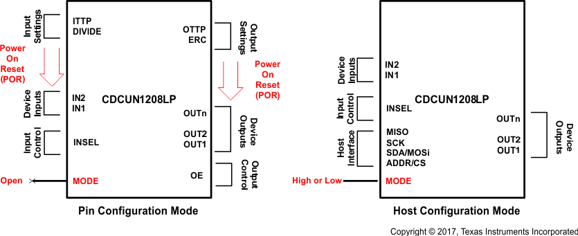
 When the host interface is enabled, certain pins take on alternative functions, according to Table 8.
Table 8. CDCUN1208LP Host Configuration Pins
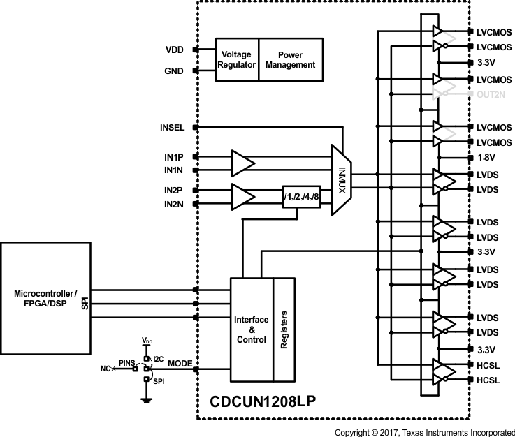
The CDCUN1208LP samples the MODE pin after the device exits the power-on reset (POR) state. The device is placed in the RESET state in one of two ways: a POR circuit automatically resets the device after power is applied; or through the RESET bit (R15[1]) in register memory (see Table 12). This RESET bit is only accessible in host configuration mode. If the MODE pin (pin 11) is open (no connection), then the device is placed in the pin configuration mode and all settings are determined by the state of various pins according to Table 1 and Figure 28. If the MODE pin is low, then device enables the SPI interface; and, if MODE is high, then I2C is enabled.
 Figure 31. CDCUN1208LP Pin and Host Configuration Mode