JAJSH89D May 2012 – April 2019 CDCUN1208LP
PRODUCTION DATA.
- 1 特長
- 2 アプリケーション
- 3 概要
- 4 改訂履歴
- 5 Pin Configuration and Functions
-
6 Specifications
- 6.1 Absolute Maximum Ratings
- 6.2 ESD Ratings
- 6.3 Recommended Operating Conditions
- 6.4 Thermal Information
- 6.5 Digital Input Electrical Characteristics – OE (SCL), INSEL, ITTP, OTTP, Divide (SDA/MOSI), ERC(ADDR/CS), Mode
- 6.6 Universal Input (IN1, IN2) Characteristics
- 6.7 Clock Output Buffer Characteristics (Output Mode = LVDS)
- 6.8 Clock Output Buffer Characteristics (Output Mode = HCSL)
- 6.9 Clock Output Buffer Electrical Characteristics (Output Mode = LVCMOS)
- 6.10 Clock Output Buffer Electrical Characteristics (Output Mode = LVCMOS) (Continued)
- 6.11 Clock Output Buffer Electrical Characteristics (Output Mode = LVCMOS) (Continued)
- 6.12 Typical Characteristics
- 7 Parameter Measurement Information
-
8 Detailed Description
- 8.1 Overview
- 8.2 Functional Block Diagrams
- 8.3 Feature Description
- 8.4 Device Functional Modes
- 8.5
Programming
- 8.5.1
Host Interface Hardware Information
- 8.5.1.1 SPI Communication
- 8.5.1.2
I2C Communication
- 8.5.1.2.1
Message Transmission
- 8.5.1.2.1.1 Data and Address Bits
- 8.5.1.2.1.2 Special Symbols – Start (S) and Stop (P)
- 8.5.1.2.1.3 Special Symbols – Acknowledge (ACK)
- 8.5.1.2.1.4 Generic Message Frame
- 8.5.1.2.1.5 CDCUN1208LP Message Format
- 8.5.1.2.1.6 CDCUN1208LP Device Addressing (I2C Address)
- 8.5.1.2.1.7 CDCUN1208LP Device Addressing (Register Address)
- 8.5.1.2.2 I2C Master and Slave Handshaking
- 8.5.1.2.3 Block Read/Write
- 8.5.1.2.4 I2C Timing
- 8.5.1.2.1
Message Transmission
- 8.5.1
Host Interface Hardware Information
- 8.6 Register Maps
- 9 Application and Implementation
- 10Power Supply Recommendations
- 11Layout
- 12デバイスおよびドキュメントのサポート
- 13メカニカル、パッケージ、および注文情報
パッケージ・オプション
メカニカル・データ(パッケージ|ピン)
- RHB|32
サーマルパッド・メカニカル・データ
- RHB|32
発注情報
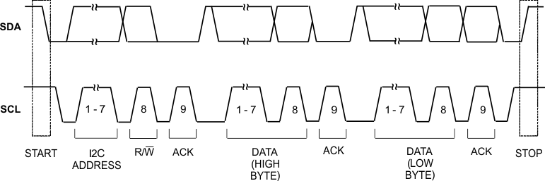
8.5.1.2.1.4 Generic Message Frame
Figure 37 shows a typical format for I2C messages. The message frame is bracketed by the START and STOP symbols (both generated by the master). If a START symbol has not been transmitted, then the bus is considered ‘available’. If a START symbol has been transmitted and a STOP symbol has not been transmitted, the bus is considered ‘busy’. The first 8 bits transmitted include the R/W bit and a 7-bit I2C address field. The reception of each byte grouping that is transmitted must be acknowledged by the receiver. Next, the high byte of the data pay load is transmitted (MSB first) followed by an acknowledgment by the receiver. Finally, the low byte is sent. After acknowledgment, the master sends a STOP symbol to end the message frame.
 Figure 37. I2C Message Format