JAJSMK8A october 2021 – june 2023 DLPA300
PRODUCTION DATA
- 1
- 1 特長
- 2 アプリケーション
- 3 概要
- 4 Revision History
- 5 Pin Configuration and Functions
-
6 Specifications
- 6.1 Absolute Maximum Ratings
- 6.2 ESD Ratings
- 6.3 Recommended Operating Conditions
- 6.4 Thermal Information
- 6.5 Electrical Characteristics Control Logic
- 6.6 5-V Linear Regulator
- 6.7 Bias Voltage Boost Converter
- 6.8 Reset Voltage Buck-Boost Converter
- 6.9 VOFFSET Regulator
- 6.10 Switching Characteristics
- 7 Detailed Description
- 8 Application and Implementation
- 9 Power Supply Recommendations
- 10Layout
- 11Device and Documentation Support
- 12Mechanical, Packaging, and Orderable Information
7.3.2 Bias Voltage Boost Converter
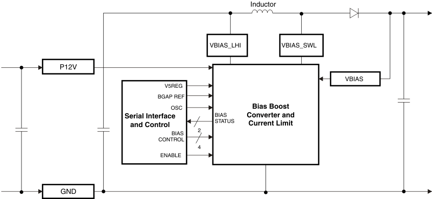
The bias voltage converter is a switching supply that operates at 1.3 MHz. The converter supplies the internal bias voltage for the high voltage FET switches. The VBIAS voltage level for the 9-μm pixel family of DMDs is 21V. The VBIAS voltage level is configured by the DLP display controller chip over the serial communication port (SCP). Four control bits select the voltage level while a fifth bit is the on/off control. The module provides two status bits to indicate latched and unlatched status bits for under-voltage (VUV) and current-limit (CL) conditions.
Figure 7-2 shows the block diagram of this module. The input decoupling capacitors are shared with other internal DLPA300 modules. See Section 8.2.2.1 for recommended component values.
 Figure 7-2 Bias Voltage Boost Converter Block
Diagram