JAJSMK8A october 2021 – june 2023 DLPA300
PRODUCTION DATA
- 1
- 1 特長
- 2 アプリケーション
- 3 概要
- 4 Revision History
- 5 Pin Configuration and Functions
-
6 Specifications
- 6.1 Absolute Maximum Ratings
- 6.2 ESD Ratings
- 6.3 Recommended Operating Conditions
- 6.4 Thermal Information
- 6.5 Electrical Characteristics Control Logic
- 6.6 5-V Linear Regulator
- 6.7 Bias Voltage Boost Converter
- 6.8 Reset Voltage Buck-Boost Converter
- 6.9 VOFFSET Regulator
- 6.10 Switching Characteristics
- 7 Detailed Description
- 8 Application and Implementation
- 9 Power Supply Recommendations
- 10Layout
- 11Device and Documentation Support
- 12Mechanical, Packaging, and Orderable Information
8.2.3 Application Curves
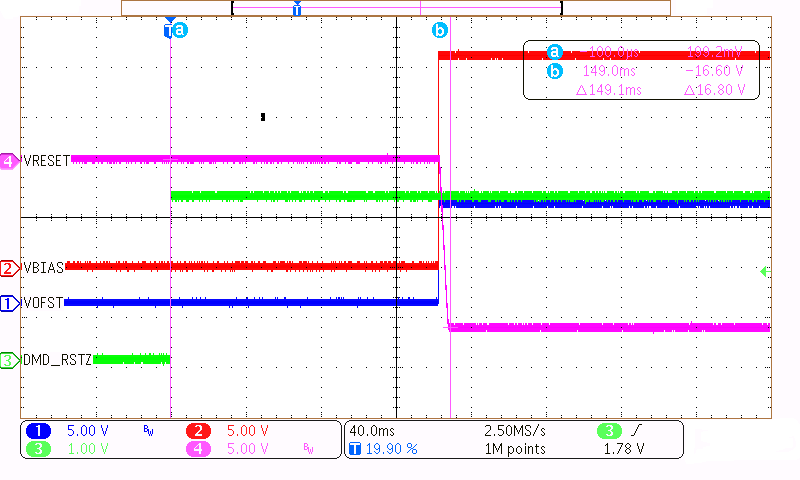
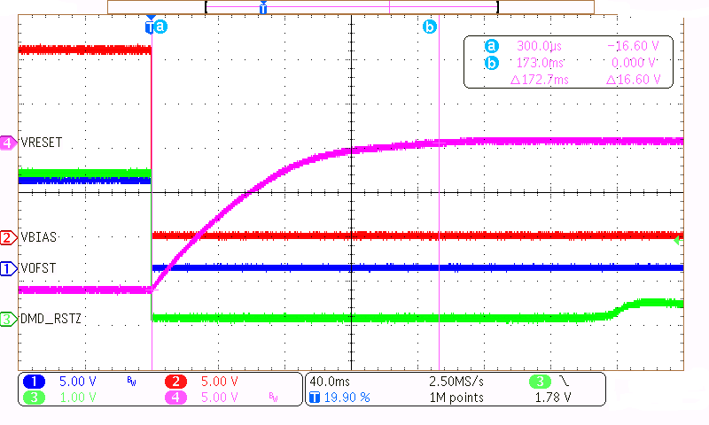
The power supply sequencing for VBIAS, VOFFSET and VRESET are shown in Figure 8-2 and Figure 8-3. On power-up, the turn on of VBIAS enables the external VRESET voltage regulator. In power-down, when VBIAS powers off, it disables the VRESET regulator, which slowly decays to ground.
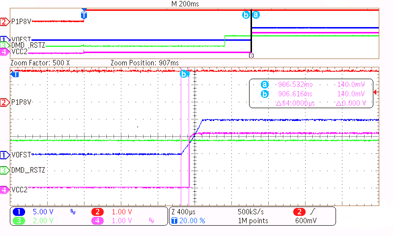
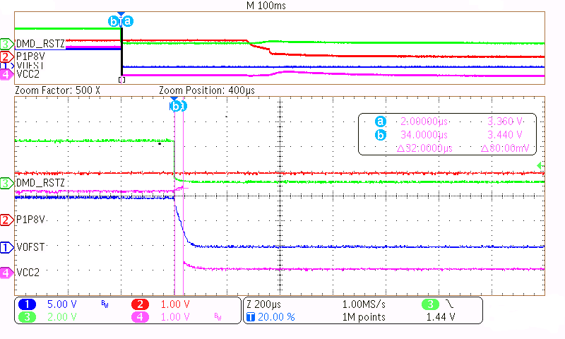
The power sequencing for VCC2 voltage regulator is shown in Figure 8-4 and Figure 8-5. The power up of VOFFSET enables the turn on of the VCC2 voltage regulator. As seen in the zoom out of Figure 8-4, the 1.8-V supply is already on and stable. Similarly, the power down of VOFFSET disables the VCC2 voltage regulator. The 1.8-V supply powers down after both VOFFSET and VCC2 are powered down, as seen in the zoom out of Figure 8-5.
 Figure 8-2 High Voltage Power-Up
Sequence
 Figure 8-4 VCC2 Power-Up
Sequence
 Figure 8-3 High Voltage Power-Down
Sequence
 Figure 8-5 VCC2 Power-Down
Sequence