JAJSU28 March 2023 DRV8329-Q1
PRODUCTION DATA
- 1
- 1 特長
- 2 アプリケーション
- 3 概要
- 4 Device Comparison Table
- 5 Pin Configuration and Functions
- 6 Specification
-
7 Detailed Description
- 7.1 Overview
- 7.2 Functional Block Diagram
- 7.3
Feature Description
- 7.3.1 Three BLDC Gate Drivers
- 7.3.2 AVDD Linear Voltage Regulator
- 7.3.3 Pin Diagrams
- 7.3.4 Low-Side Current Sense Amplifiers
- 7.3.5 Gate Driver Shutdown Sequence (DRVOFF)
- 7.3.6
Gate Driver Protective Circuits
- 7.3.6.1 PVDD Supply Undervoltage Lockout (PVDD_UV)
- 7.3.6.2 AVDD Power on Reset (AVDD_POR)
- 7.3.6.3 GVDD Undervoltage Lockout (GVDD_UV)
- 7.3.6.4 BST Undervoltage Lockout (BST_UV)
- 7.3.6.5 MOSFET VDS Overcurrent Protection (VDS_OCP)
- 7.3.6.6 VSENSE Overcurrent Protection (SEN_OCP)
- 7.3.6.7 Thermal Shutdown (OTSD)
- 7.4 Device Functional Modes
-
8 Application and Implementation
- 8.1 Application Information
- 8.2
Typical Application
- 8.2.1
Three Phase Brushless-DC Motor Control
- 8.2.1.1
Detailed Design Procedure
- 8.2.1.1.1 Motor Voltage
- 8.2.1.1.2 Bootstrap Capacitor and GVDD Capacitor Selection
- 8.2.1.1.3 Gate Drive Current
- 8.2.1.1.4 Gate Resistor Selection
- 8.2.1.1.5 System Considerations in High Power Designs
- 8.2.1.1.6 Dead Time Resistor Selection
- 8.2.1.1.7 VDSLVL Selection
- 8.2.1.1.8 AVDD Power Losses
- 8.2.1.1.9 Current Sensing and Output Filtering
- 8.2.1.1.10 Power Dissipation and Junction Temperature Losses
- 8.2.1.1
Detailed Design Procedure
- 8.2.2 Application Curves
- 8.2.1
Three Phase Brushless-DC Motor Control
- 8.3 Power Supply Recommendations
- 8.4 Layout
- 9 Device and Documentation Support
- 10Revision History
- 11Mechanical, Packaging, and Orderable Information
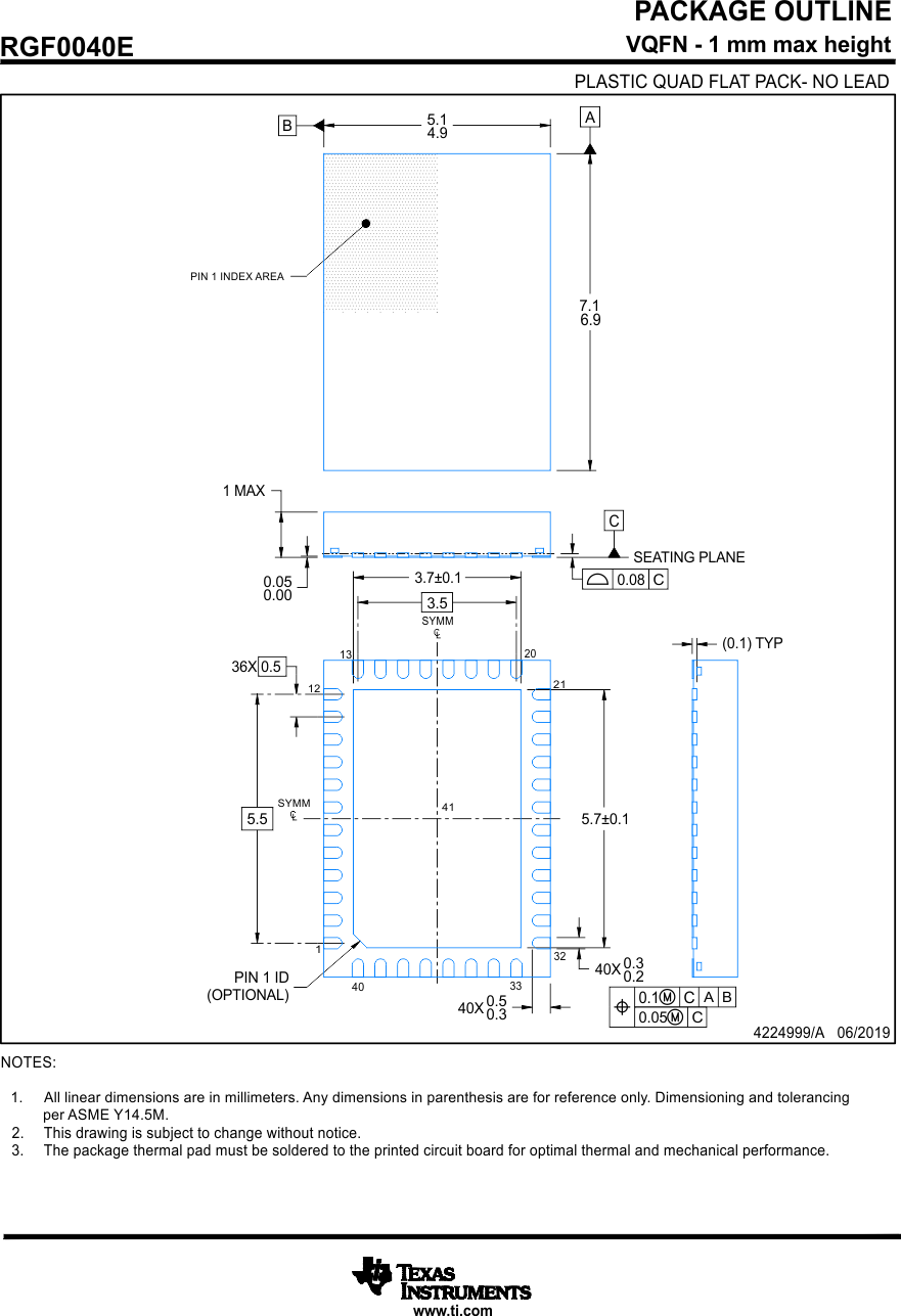
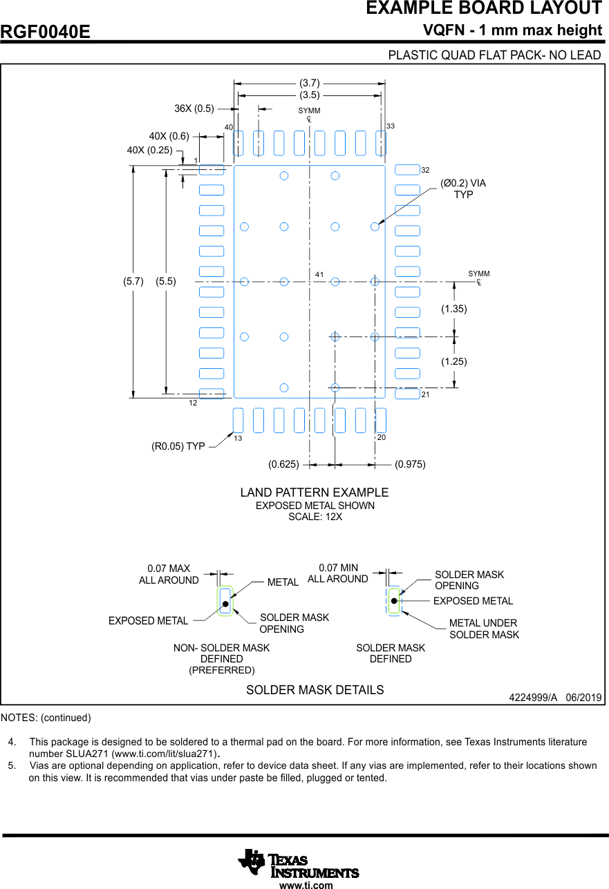
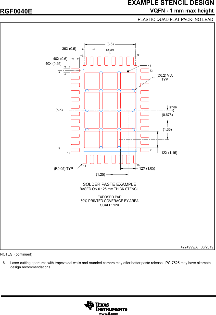
11 Mechanical, Packaging, and Orderable Information
The following pages include mechanical, packaging, and orderable information. This information is the most-current data available for the designated device. This data is subject to change without notice and without revision of this document. For browser-based versions of this data sheet, see the left-hand navigation pane.