JAJSGB0 September 2018 DSLVDS1047
PRODUCTION DATA.
6.7 Typical Characteristics
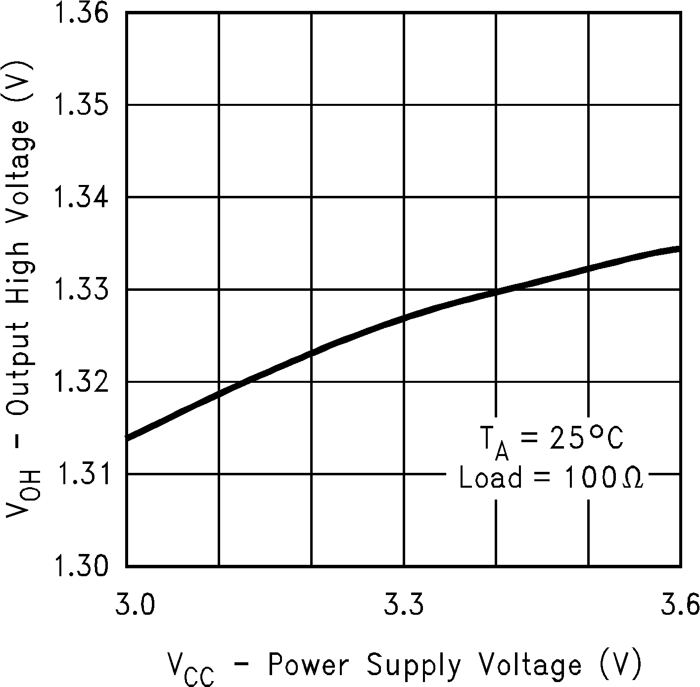 Figure 1. Output High Voltage vs Power Supply Voltage
 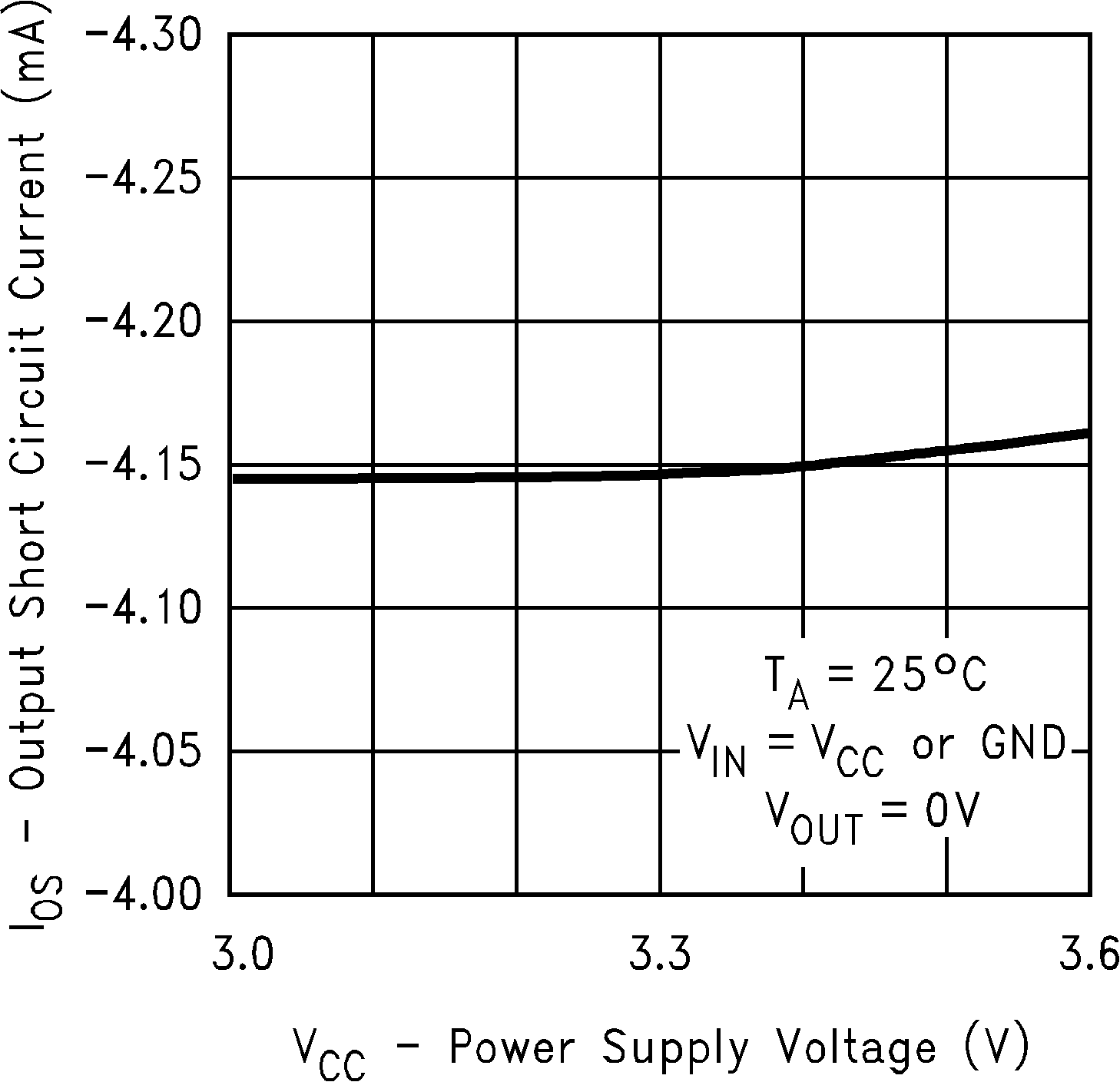 Figure 3. Output Short Circuit Current vs
Power Supply Voltage
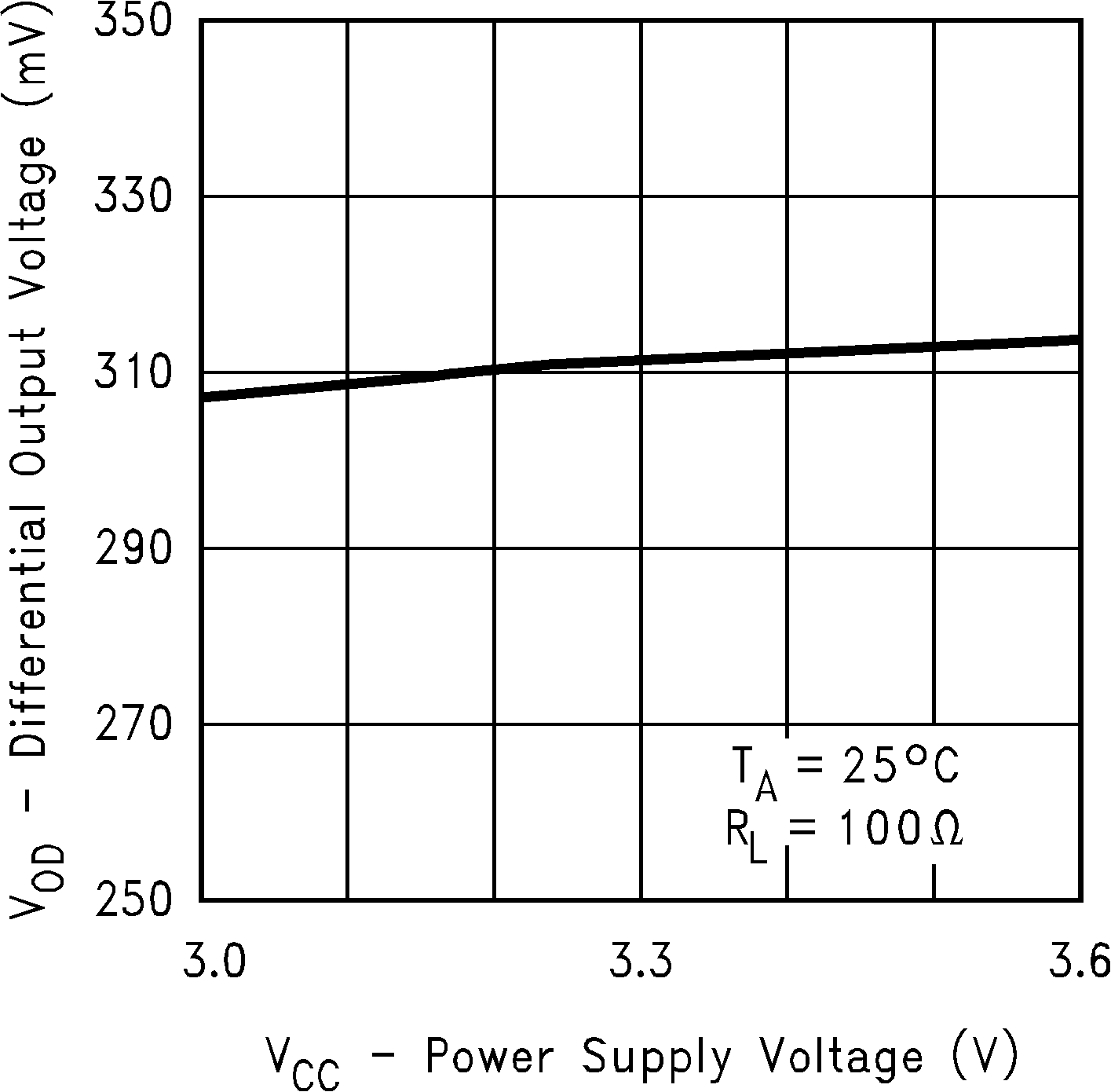 Figure 5. Differential Output Voltage vs
Power Supply Voltage
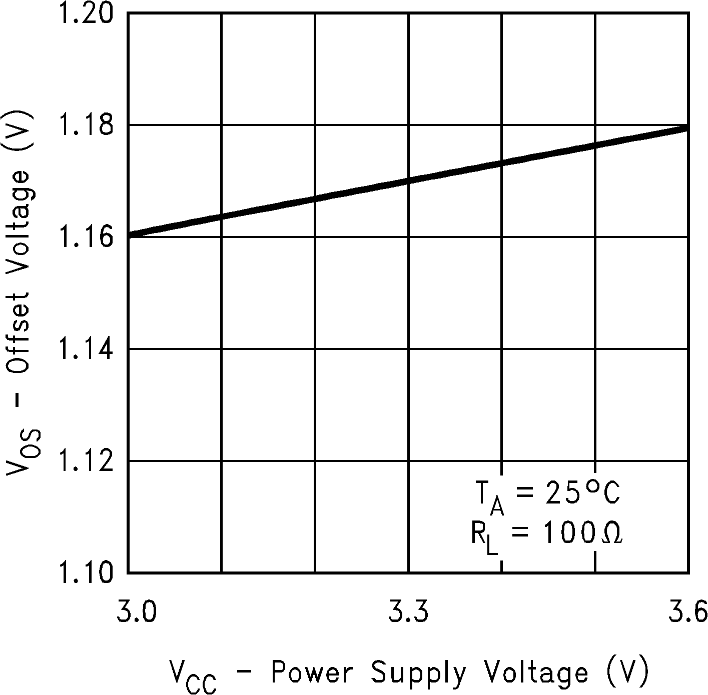 Figure 7. Offset Voltage vs Power Supply Voltage
 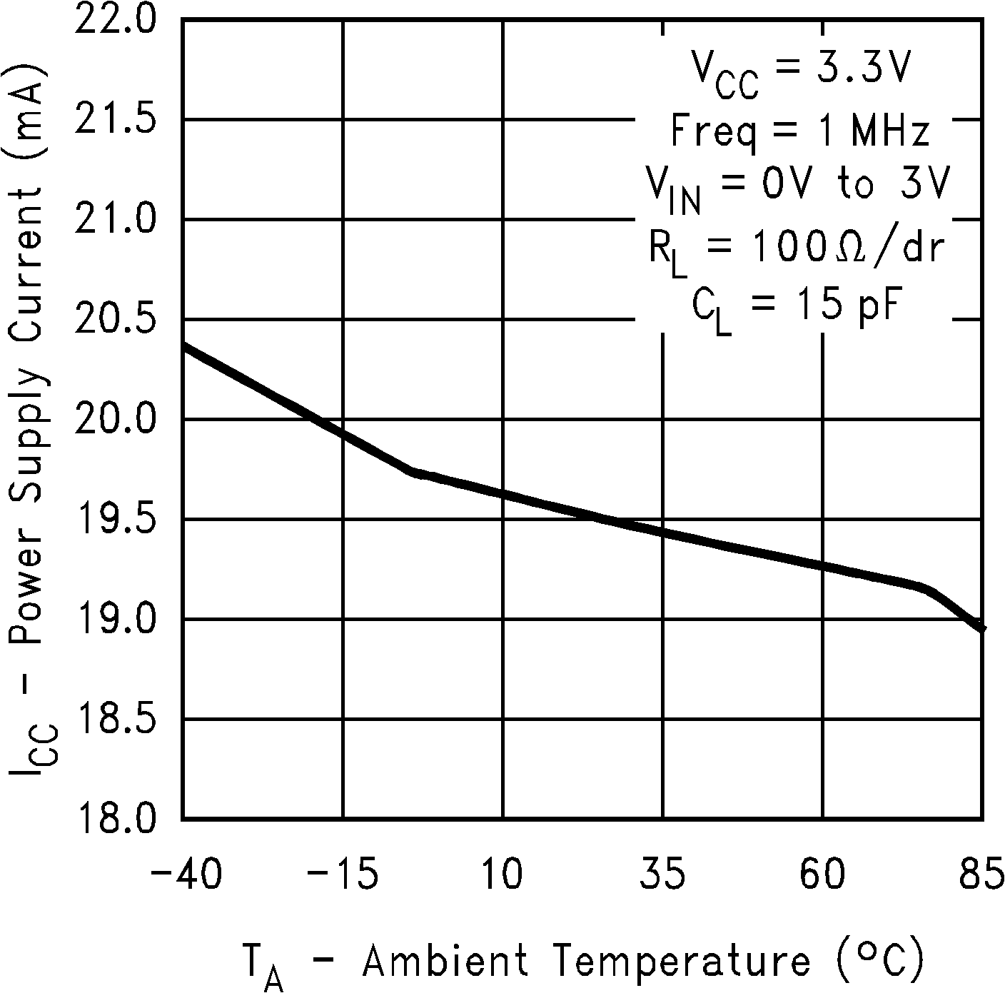 Figure 9. Power Supply Current vs Ambient Temperature
 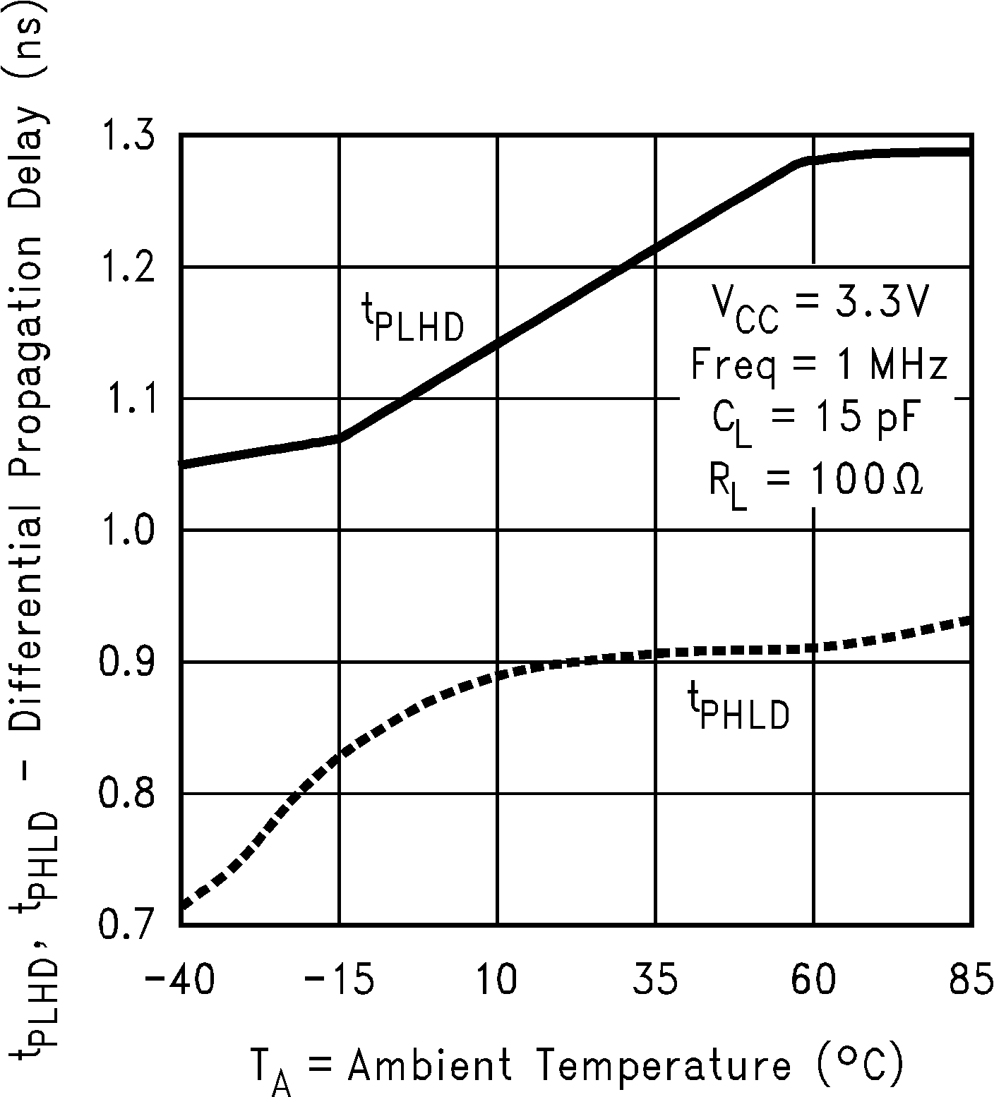 Figure 11. Differential Propagation Delay vs
Ambient Temperature
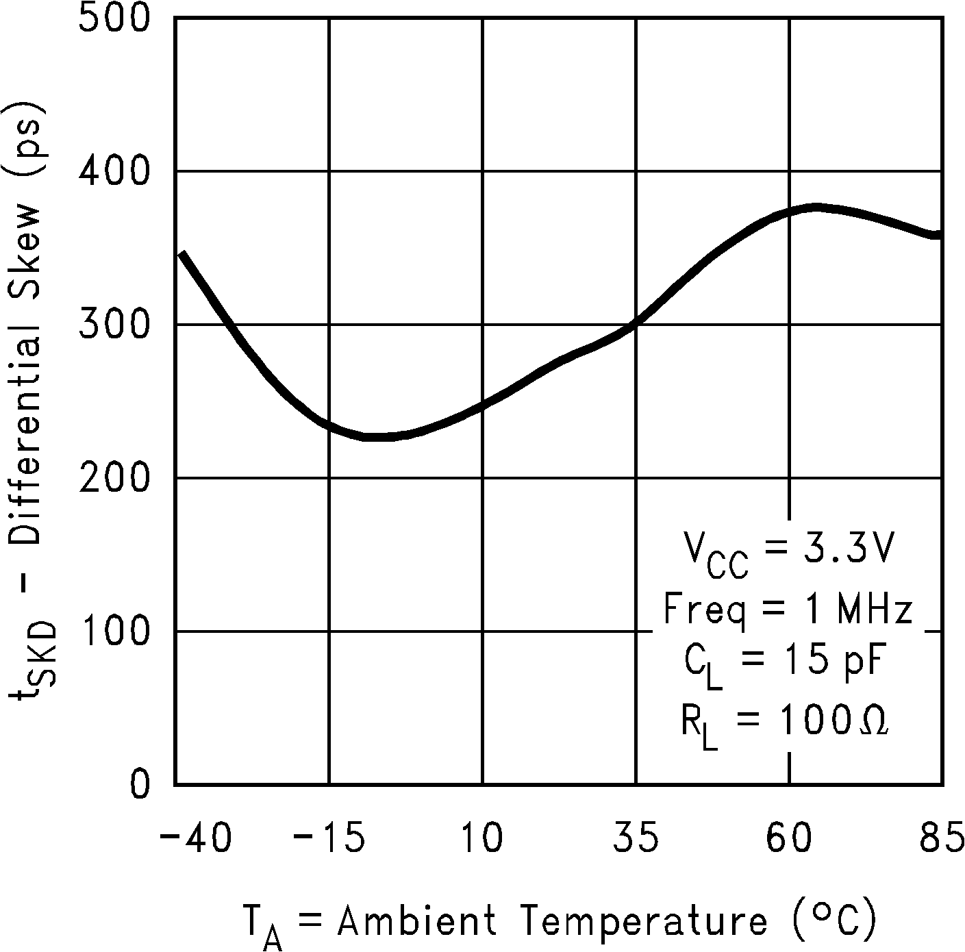 Figure 13. Differential Skew vs Ambient Temperature
 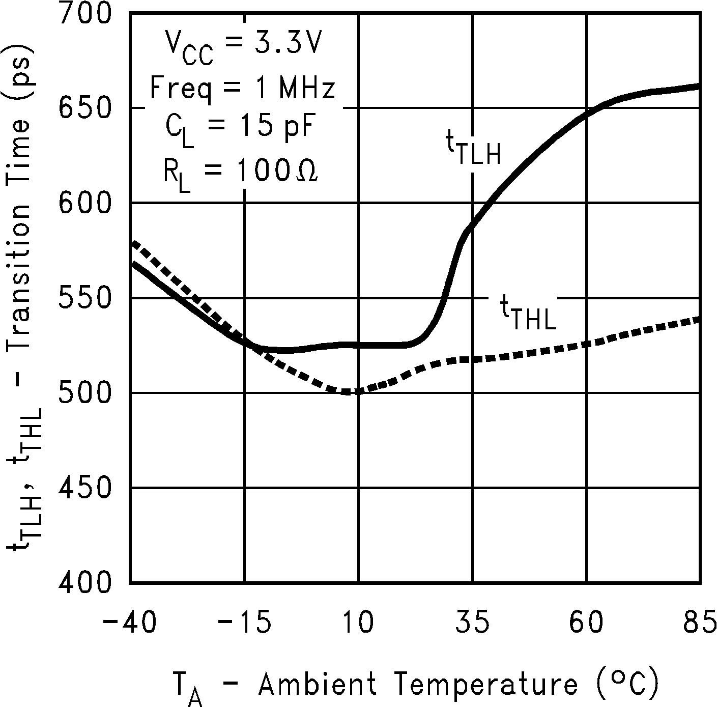 Figure 15. Transition Time vs Ambient Temperature
 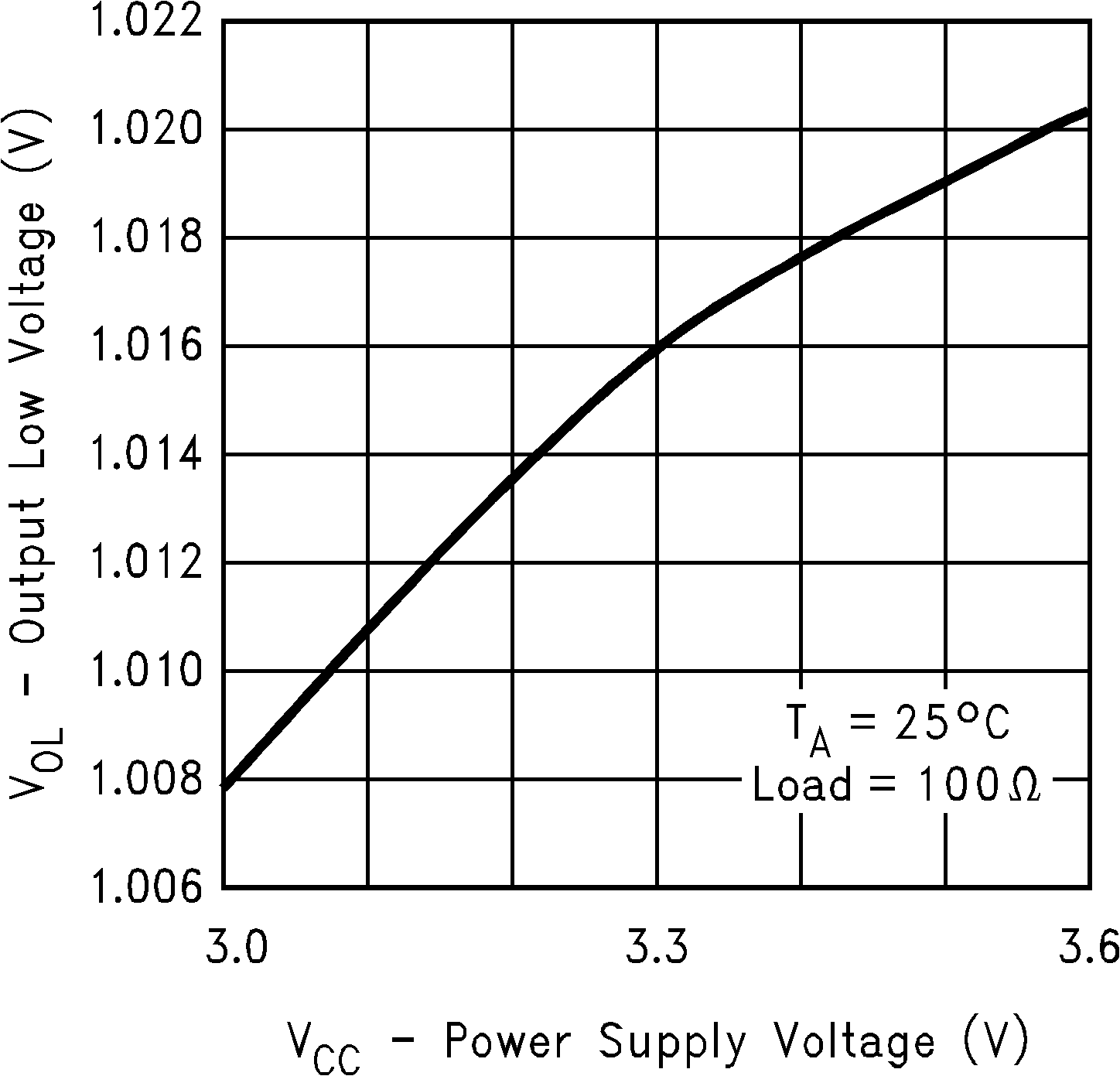 Figure 2. Output Low Voltage vs Power Supply Voltage
 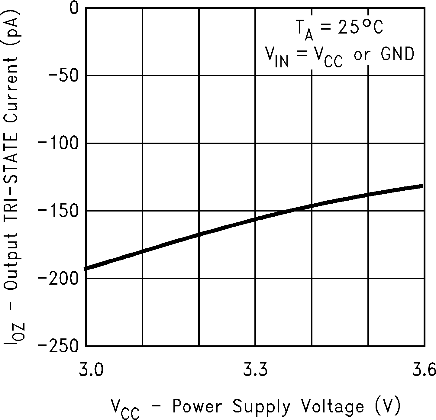 Figure 4. Output TRI-STATE Current vs
Power Supply Voltage
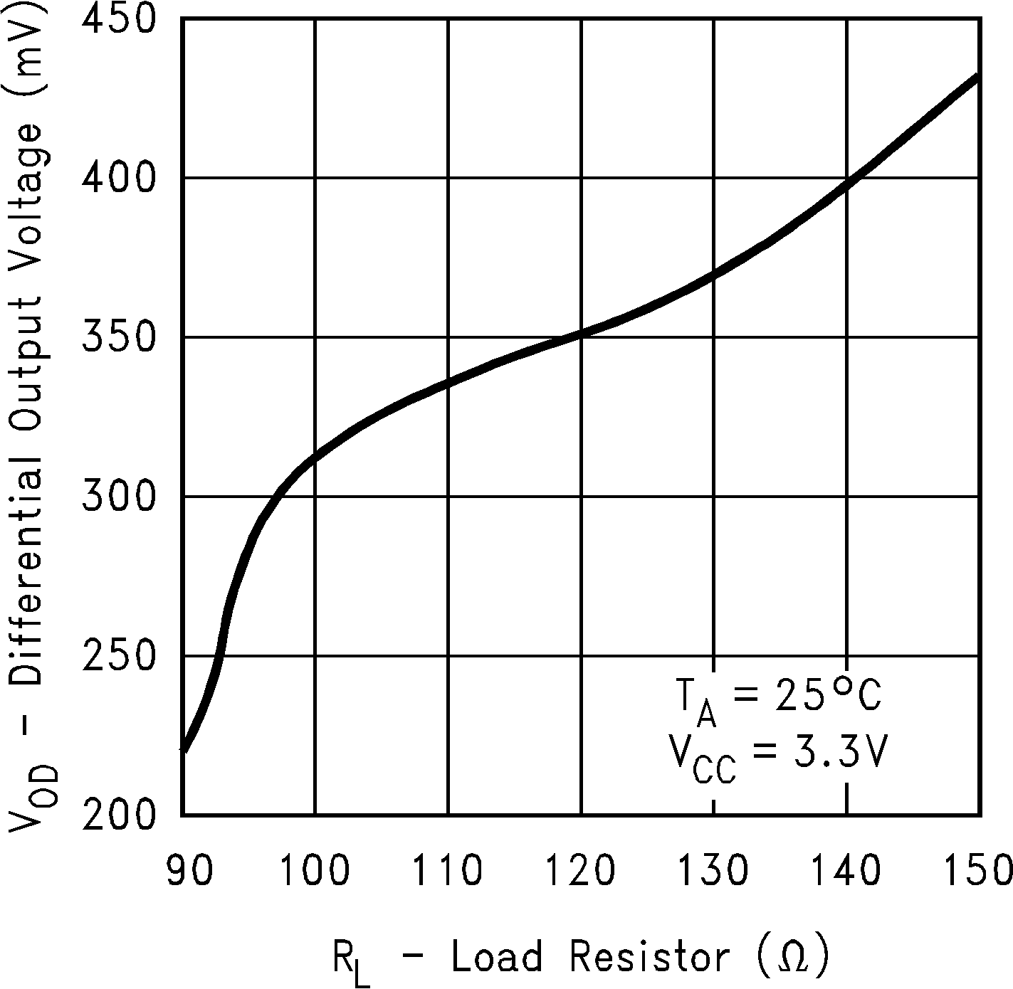 Figure 6. Differential Output Voltage vs Load Resistor
 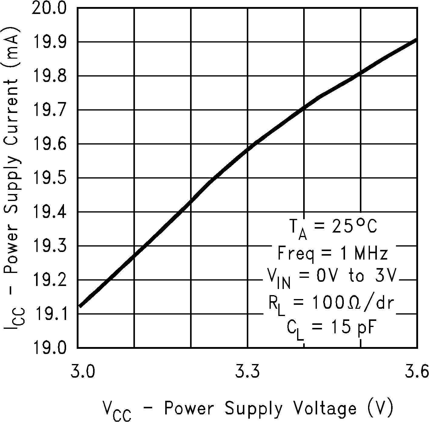 Figure 8. Power Supply Current vs Power Supply Voltage
 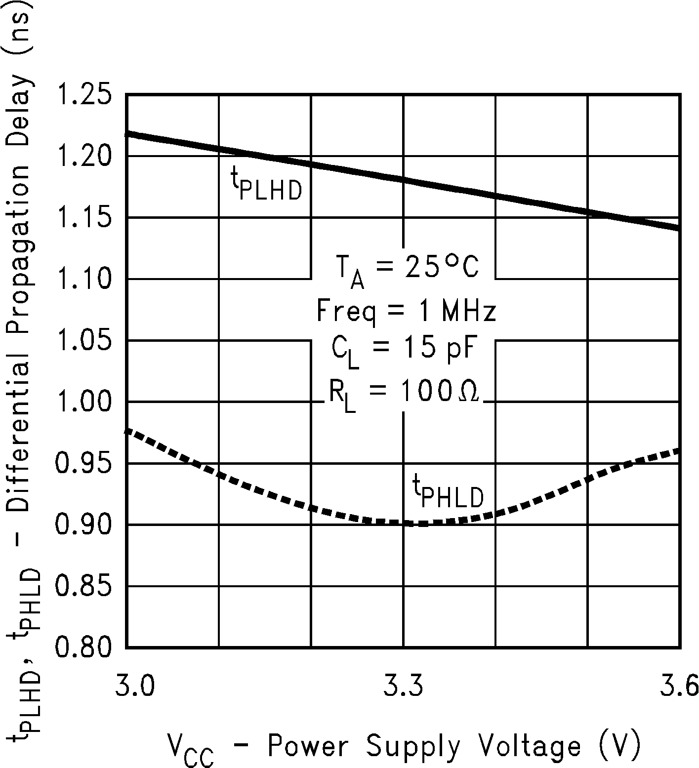 Figure 10. Differential Propagation Delay vs
Power Supply Voltage
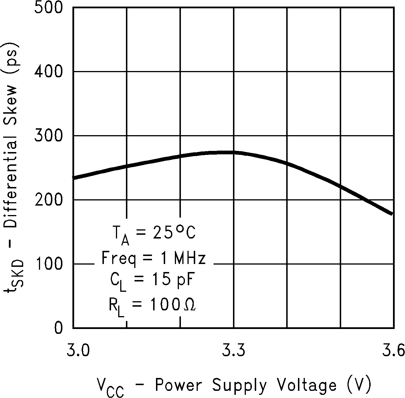 Figure 12. Differential Skew vs Power Supply Voltage
 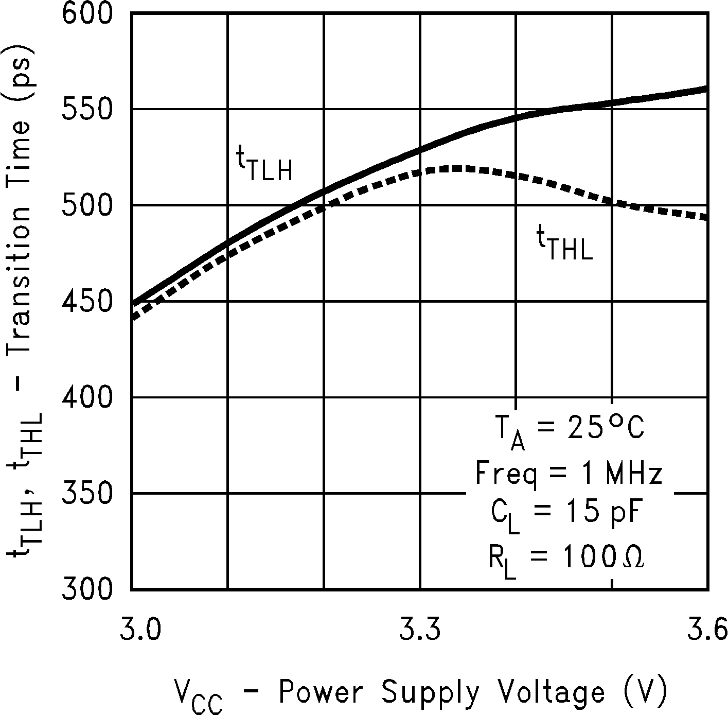 Figure 14. Transition Time vs Power Supply Voltage
 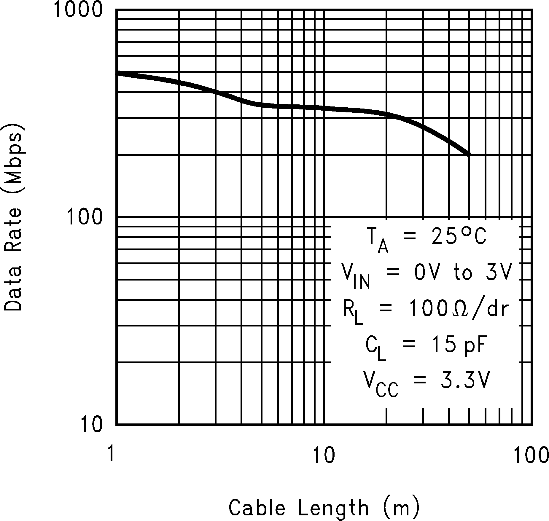 Figure 16. Data Rate vs Cable Length