JAJSGB0 September 2018 DSLVDS1047
PRODUCTION DATA.
8.3.1 LVDS Fail-Safe
This section addresses the common concern of fail-safe biasing of LVDS interconnects, specifically looking at the DSLVDS1047 driver outputs and the DSLVDS1048 receiver inputs.
The LVDS receiver is a high-gain, high-speed device that amplifies a small differential signal (20 mV) to CMOS logic levels. Due to the high gain and tight threshold of the receiver, take care to prevent noise from appearing as a valid signal.
The internal fail-safe circuitry of the receiver is designed to source or sink a small amount of current, providing fail-safe protection (a stable known state of HIGH output voltage) for floating, terminated, or shorted receiver inputs.
- Open Input Pins. The DSLVDS1048 is a quad receiver device, and if an application requires only 1, 2, or 3 receivers, the unused channel(s) inputs must be left OPEN. Do not tie unused receiver inputs to ground or any other voltages. The input is biased by internal high value pullup and pulldown resistors to set the output to a HIGH state. This internal circuitry ensures a HIGH, stable output state for open inputs.
- Terminated Input. If the DSLVDS1047 driver is disconnected (cable unplugged), or if the DSLVDS1047 driver is in a TRI-STATE or power-off condition, the receiver output is again in a HIGH state, even with the end of cable 100-Ω termination resistor across the input pins. The unplugged cable can become a floating antenna which can pick up noise. If the cable picks up more than 10 mV of differential noise, the receiver may see the noise as a valid signal and switch. To insure that any noise is seen as common-mode and not differential, a balanced interconnect must be used. Twisted pair cable offers better balance than flat ribbon cable.
- Shorted Inputs. If a fault condition occurs that shorts the receiver inputs together, thus resulting in a 0-V differential input voltage, the receiver output remains in a HIGH state. Shorted input fail-safe is not supported across the common-mode range of the device (GND to 2.4 V). It is only supported with inputs shorted and no external common-mode voltage applied.
External lower value pullup and pulldown resistors (for a stronger bias) may be used to boost fail-safe in the presence of higher noise levels. The pullup and pulldown resistors should be in the 5-kΩ to 15-kΩ range to minimize loading and waveform distortion to the driver. The common-mode bias point should be set to approximately 1.2 V (less than 1.75 V) to be compatible with the internal circuitry.
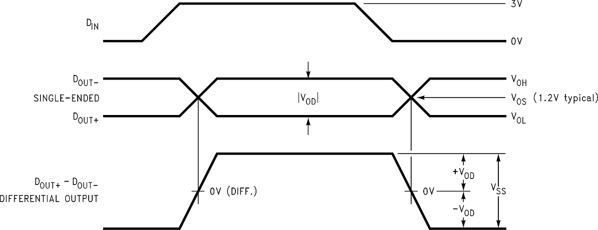
 Figure 22. Driver Output Levels