JAJSGB0 September   2018 DSLVDS1047

PRODUCTION DATA.  

  1. 特長
  2. アプリケーション
  3. 概要
    1.     Device Images
      1. 3.1 アプリケーション図
  4. 改訂履歴
  5. Pin Configuration and Functions
    1.     Pin Functions
  6. Specifications
    1. 6.1 Absolute Maximum Ratings
    2. 6.2 ESD Ratings
    3. 6.3 Recommended Operating Conditions
    4. 6.4 Thermal Information
    5. 6.5 Electrical Characteristics
    6. 6.6 Switching Characteristics
    7. 6.7 Typical Characteristics
  7. Parameter Measurement Information
  8. Detailed Description
    1. 8.1 Overview
    2. 8.2 Functional Block Diagram
    3. 8.3 Feature Description
      1. 8.3.1 LVDS Fail-Safe
    4. 8.4 Device Functional Modes
  9. Application and Implementation
    1. 9.1 Application Information
    2. 9.2 Typical Application
      1. 9.2.1 Design Requirements
      2. 9.2.2 Detailed Design Procedure
        1. 9.2.2.1 Probing LVDS Transmission Lines
        2. 9.2.2.2 Data Rate vs Cable Length Graph Test Procedure
      3. 9.2.3 Application Curve
  10. 10Power Supply Recommendations
  11. 11Layout
    1. 11.1 Layout Guidelines
      1. 11.1.1 Power Decoupling Recommendations
      2. 11.1.2 Differential Traces
      3. 11.1.3 Termination
    2. 11.2 Layout Example
  12. 12デバイスおよびドキュメントのサポート
    1. 12.1 ドキュメントの更新通知を受け取る方法
    2. 12.2 コミュニティ・リソース
    3. 12.3 商標
    4. 12.4 静電気放電に関する注意事項
    5. 12.5 Glossary
  13. 13メカニカル、パッケージ、および注文情報

パッケージ・オプション

メカニカル・データ(パッケージ|ピン)
サーマルパッド・メカニカル・データ
発注情報

Parameter Measurement Information

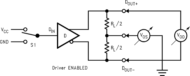
DSLVDS1047 10088703.pngFigure 17. Driver VOD and VOS Test Circuit
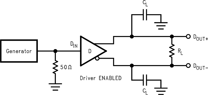
DSLVDS1047 10088704.pngFigure 18. Driver Propagation Delay and Transition Time Test Circuit
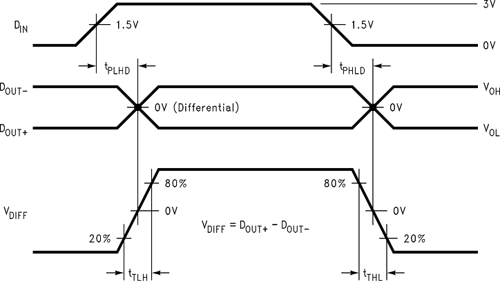
DSLVDS1047 10088705.pngFigure 19. Driver Propagation Delay and Transition Time Waveforms
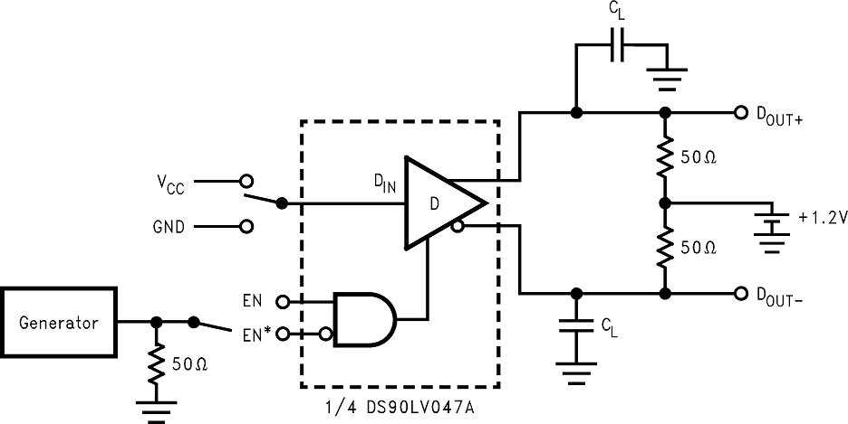
DSLVDS1047 10088706.pngFigure 20. Driver TRI-STATE Delay Test Circuit
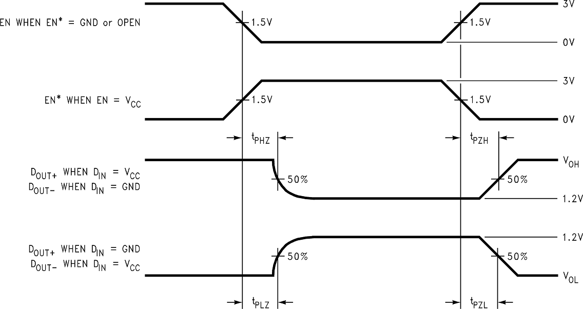
DSLVDS1047 10088707.pngFigure 21. Driver TRI-STATE Delay Waveform