SNOSCZ7B December   2015  – April 2024 LDC0851

PRODUCTION DATA  

  1.   1
  2. Features
  3. Applications
  4. Description
  5. Pin Configuration and Functions
  6. Specifications
    1. 5.1 Absolute Maximum Ratings
    2. 5.2 ESD Ratings
    3. 5.3 Recommended Operating Conditions
    4. 5.4 Thermal Information
    5. 5.5 Electrical Characteristics
    6. 5.6 Interface Voltage Levels
    7. 5.7 Timing Requirements
    8. 5.8 Typical Characteristics
  7. Detailed Description
    1. 6.1 Overview
    2. 6.2 Functional Block Diagram
    3. 6.3 Feature Description
      1. 6.3.1 Basic Operation Mode
      2. 6.3.2 Threshold Adjust Mode
      3. 6.3.3 Setting the Threshold Adjust Values
      4. 6.3.4 Hysteresis
      5. 6.3.5 Conversion Time
      6. 6.3.6 Power-Up Conditions
    4. 6.4 Device Functional Modes
      1. 6.4.1 Shutdown Mode
      2. 6.4.2 Active Mode
  8. Application and Implementation
    1. 7.1 Application Information
      1. 7.1.1 Sensor Design
        1. 7.1.1.1 Sensor Frequency
        2. 7.1.1.2 Sensor Design Procedure
    2. 7.2 Typical Application
      1. 7.2.1 Event Counting
        1. 7.2.1.1 Design Requirements
        2. 7.2.1.2 Detailed Design Procedure
        3. 7.2.1.3 Application Curves
      2. 7.2.2 Coarse Position Sensing
        1. 7.2.2.1 Design Requirements
        2. 7.2.2.2 Detailed Design Procedure
        3. 7.2.2.3 Application Curves
      3. 7.2.3 Low Power Operation
        1. 7.2.3.1 Design Requirements
        2. 7.2.3.2 Detailed Design Procedure
        3. 7.2.3.3 Application Curves
    3. 7.3 Power Supply Recommendations
    4. 7.4 Layout
      1. 7.4.1 Layout Guidelines
      2. 7.4.2 Layout Example
        1. 7.4.2.1 Side by Side Coils
        2. 7.4.2.2 Stacked Coils
  9. Device and Documentation Support
    1. 8.1 Device Support
      1. 8.1.1 Development Support
    2. 8.2 Documentation Support
      1. 8.2.1 Related Documentation
    3. 8.3 Support Resources
    4. 8.4 Trademarks
    5. 8.5 Electrostatic Discharge Caution
    6. 8.6 Glossary
  10. Revision History
  11. 10Mechanical, Packaging, and Orderable Information

パッケージ・オプション

メカニカル・データ(パッケージ|ピン)
サーマルパッド・メカニカル・データ
発注情報

Sensor Design

The LDC0851 relies on two externally placed sensors (LSENSE and LREF) and a capacitor (CSENSOR) for proper operation. The design and matching of the coils is very critical to ensure a proper switching occurrence. It is also important to note that the parasitic capacitance of the board (CBOARD) and of the LCOM input pin (CIN_COM) are in parallel with CSENSOR, and the sum of all three capacitances create a total capacitance (CTOTAL) which is considered part of the system. CTOTAL must be greater than 33 pF to be considered in the valid design space.
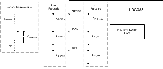
GUID-AD83BCD5-C55B-4A46-99C5-0A93A4441FF0-low.gifFigure 7-1 Sensor Components, Board Parasitics, and Package Parasitics Diagram