JAJSUC2B December 2015 – April 2024 LDC0851
PRODUCTION DATA
- 1
- 1 特長
- 2 アプリケーション
- 3 概要
- 4 Pin Configuration and Functions
- 5 Specifications
- 6 Detailed Description
- 7 Application and Implementation
- 8 Device and Documentation Support
- 9 Revision History
- 10Mechanical, Packaging, and Orderable Information
パッケージ・オプション
メカニカル・データ(パッケージ|ピン)
- DSG|8
サーマルパッド・メカニカル・データ
- DSG|8
発注情報
7.1.1.2 Sensor Design Procedure
The following procedure should be followed for determining the sensor characteristics:
- Determine the diameter of coil (dcoil), which should be 3 times larger than the desired switching distance (dswitch)
- Determine the desired frequency (ƒSENSOR) which should be between 300 kHz and 19 MHz
- Calculate the range of allowable inductance from the following equation:
Equation 7.
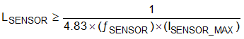
where:
- LSENSOR is the inductance of the LSENSE coil or LREF coil
- ISENSOR_MAX is given in the electrical table
- Calculate the externally placed sensor capacitor:
Equation 8. 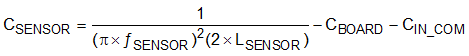
where:
- CBOARD is the parasitic capacitance introduced by the board layout (~4 pF for good layout)
- CIN_COM is the parasitic pin capacitance of LCOM specified as 12 pF in the electrical table