JAJSRS8I February   2007  – November 2023 LM5116

PRODUCTION DATA  

  1.   1
  2. 特長
  3. アプリケーション
  4. 概要
  5. Pin Configuration and Functions
  6. Specifications
    1. 5.1 Absolute Maximum Ratings
    2. 5.2 ESD Ratings
    3. 5.3 Recommended Operating Conditions
    4. 5.4 Thermal Information
    5. 5.5 Electrical Characteristics
    6. 5.6 Switching Characteristics
    7. 5.7 Typical Performance Characteristics
  7. Detailed Description
    1. 6.1 Overview
    2. 6.2 Functional Block Diagram
    3. 6.3 Feature Description
      1. 6.3.1 High Voltage Start-Up Regulator
      2. 6.3.2 Enable
      3. 6.3.3 UVLO
      4. 6.3.4 Oscillator and Sync Capability
      5. 6.3.5 Error Amplifier and PWM Comparator
      6. 6.3.6 Ramp Generator
      7. 6.3.7 Current Limit
      8. 6.3.8 HO Output
      9. 6.3.9 Thermal Protection
    4. 6.4 Device Functional Modes
      1. 6.4.1 Soft-Start and Diode Emulation
  8. Application and Implementation
    1. 7.1 Application Information
    2. 7.2 Typical Application
      1. 7.2.1 Design Requirements
      2. 7.2.2 Detailed Design Procedure
        1. 7.2.2.1  Custom Design with WEBENCH® Tools
        2. 7.2.2.2  Timing Resistor
        3. 7.2.2.3  Output Inductor
        4. 7.2.2.4  Current Sense Resistor
        5. 7.2.2.5  Ramp Capacitor
        6. 7.2.2.6  Output Capacitors
        7. 7.2.2.7  Input Capacitors
        8. 7.2.2.8  VCC Capacitor
        9. 7.2.2.9  Bootstrap Capacitor
        10. 7.2.2.10 Soft Start Capacitor
        11. 7.2.2.11 Output Voltage Divider
        12. 7.2.2.12 UVLO Divider
        13. 7.2.2.13 MOSFETs
        14. 7.2.2.14 MOSFET Snubber
        15. 7.2.2.15 Error Amplifier Compensation
        16. 7.2.2.16 Comprehensive Equations
          1. 7.2.2.16.1 Current Sense Resistor and Ramp Capacitor
          2. 7.2.2.16.2 Modulator Transfer Function
          3. 7.2.2.16.3 Error Amplifier Transfer Function
      3. 7.2.3 Application Curves
    3. 7.3 Power Supply Recommendations
    4. 7.4 Layout
      1. 7.4.1 Layout Guidelines
      2. 7.4.2 Layout Example
  9. Device and Documentation Support
    1. 8.1 Device Support
      1. 8.1.1 サード・パーティ製品に関する免責事項
      2. 8.1.2 Development Support
        1. 8.1.2.1 Custom Design with WEBENCH® Tools
    2. 8.2 ドキュメントの更新通知を受け取る方法
    3. 8.3 サポート・リソース
    4. 8.4 Trademarks
    5. 8.5 静電気放電に関する注意事項
    6. 8.6 用語集
  10. Revision History
  11. 10Mechanical, Packaging, and Orderable Information

パッケージ・オプション

メカニカル・データ(パッケージ|ピン)
サーマルパッド・メカニカル・データ
発注情報

Current Sense Resistor

The current limit is set by the current sense resistor value (RS).

Equation 46. GUID-4F4DB949-70F0-4C3D-9D19-FE1B7ECF22F0-low.gif

For a 5V output, the maximum current sense signal occurs at the minimum input voltage, so RS is calculated from:

Equation 34. GUID-AC919622-3E59-43A5-ABE0-D0016FF70C49-low.gif

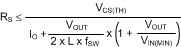
For this example VCCX = 0 V, so VCS(TH) = 0.11 V. The current sense resistor is calculated as:

Equation 35. GUID-FDC3CA53-E64E-49A8-9378-147794F7C8E2-low.gif

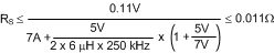
The next lowest standard value of 10 mΩ was chosen for RS.