JAJSRS8I February 2007 – November 2023 LM5116
PRODUCTION DATA
- 1
- 1 特長
- 2 アプリケーション
- 3 概要
- 4 Pin Configuration and Functions
- 5 Specifications
- 6 Detailed Description
-
7 Application and Implementation
- 7.1 Application Information
- 7.2
Typical Application
- 7.2.1 Design Requirements
- 7.2.2
Detailed Design Procedure
- 7.2.2.1 Custom Design with WEBENCH® Tools
- 7.2.2.2 Timing Resistor
- 7.2.2.3 Output Inductor
- 7.2.2.4 Current Sense Resistor
- 7.2.2.5 Ramp Capacitor
- 7.2.2.6 Output Capacitors
- 7.2.2.7 Input Capacitors
- 7.2.2.8 VCC Capacitor
- 7.2.2.9 Bootstrap Capacitor
- 7.2.2.10 Soft Start Capacitor
- 7.2.2.11 Output Voltage Divider
- 7.2.2.12 UVLO Divider
- 7.2.2.13 MOSFETs
- 7.2.2.14 MOSFET Snubber
- 7.2.2.15 Error Amplifier Compensation
- 7.2.2.16 Comprehensive Equations
- 7.2.3 Application Curves
- 7.3 Power Supply Recommendations
- 7.4 Layout
- 8 Device and Documentation Support
- 9 Revision History
- 10Mechanical, Packaging, and Orderable Information
7.2.2.7 Input Capacitors
The regulator supply voltage has a large source impedance at the switching frequency. Good quality input capacitors are necessary to limit the ripple voltage at the VIN pin while supplying most of the switch current during the on-time. When the buck switch turns on, the current into the switch steps to the valley of the inductor current waveform, ramps up to the peak value, and then drops to zero at turnoff. The input capacitors must be selected for RMS current rating and minimum ripple voltage. A good approximation for the required ripple current rating is IRMS > IOUT / 2.
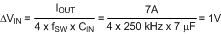
Quality ceramic capacitors with a low ESR were selected for the input filter. To allow for capacitor tolerances and voltage rating, four 2.2-µF, 100-V ceramic capacitors were used for the typical application circuit. With ceramic capacitors, the input ripple voltage will be triangular and peak at 50% duty cycle. Taking into account the capacitance change with DC bias, the input ripple voltage is approximated as:
When the converter is connected to an input power source, a resonant circuit is formed by the line impedance and the input capacitors. If step input voltage transients are expected near the maximum rating of the LM5116, a careful evaluation of the ringing and possible overshoot at the device VIN pin must be completed. To minimize overshoot make CIN > 10 ✕ LIN. The characteristic source impedance and resonant frequency are:
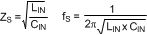
The converter exhibits a negative input impedance which is lowest at the minimum input voltage:

The damping factor for the input filter is given by:
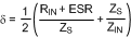
where
- RIN is the input wiring resistance
- ESR is the series resistance of the input capacitors
The term ZS / ZIN will always be negative due to ZIN.
When δ = 1, the input filter is critically damped. This can be difficult to achieve with practical component values. With δ < 0.2, the input filter will exhibit significant ringing. If δ is zero or negative, there is not enough resistance in the circuit and the input filter will sustain an oscillation. When operating near the minimum input voltage, an aluminum electrolytic capacitor across CIN can be needed to damp the input for a typical bench test setup. Any parallel capacitor must be evaluated for its RMS current rating. The current will split between the ceramic and aluminum capacitors based on the relative impedance at the switching frequency.