JAJSIW6E March 2020 – April 2022 LM62440-Q1
PRODUCTION DATA
- 1 特長
- 2 アプリケーション
- 3 概要
- 4 Revision History
- 5 概要 (続き)
- 6 Device Comparison Table
- 7 Pin Configuration and Functions
- 8 Specifications
-
9 Detailed Description
- 9.1 Overview
- 9.2 Functional Block Diagram
- 9.3
Feature Description
- 9.3.1 EN Uses for Enable and VIN UVLO
- 9.3.2 MODE/SYNC Pin Operation
- 9.3.3 PGOOD Output Operation
- 9.3.4 Internal LDO, VCC UVLO, and BIAS Input
- 9.3.5 Bootstrap Voltage and VCBOOT-UVLO (CBOOT Pin)
- 9.3.6 Adjustable SW Node Slew Rate
- 9.3.7 Spread Spectrum
- 9.3.8 Soft Start and Recovery From Dropout
- 9.3.9 Output Voltage Setting
- 9.3.10 Overcurrent and Short Circuit Protection
- 9.3.11 Thermal Shutdown
- 9.3.12 Input Supply Current
- 9.4 Device Functional Modes
-
10Application and Implementation
- 10.1 Application Information
- 10.2
Typical Application
- 10.2.1 Design Requirements
- 10.2.2
Detailed Design Procedure
- 10.2.2.1 Choosing the Switching Frequency
- 10.2.2.2 Setting the Output Voltage
- 10.2.2.3 Inductor Selection
- 10.2.2.4 Output Capacitor Selection
- 10.2.2.5 Input Capacitor Selection
- 10.2.2.6 BOOT Capacitor
- 10.2.2.7 BOOT Resistor
- 10.2.2.8 VCC
- 10.2.2.9 BIAS
- 10.2.2.10 CFF and RFF Selection
- 10.2.2.11 External UVLO
- 10.2.3 Application Curves
- 11Power Supply Recommendations
- 12Layout
- 13Device and Documentation Support
- 14Mechanical, Packaging, and Orderable Information
10.2.3 Application Curves
Unless otherwise specified, the following conditions apply: VIN
= 13.5 V, TA = 25°C. The circuit is shown in Figure 10-1, with
the appropriate BOM from Table 10-5.
Unless otherwise specified, the following conditions apply: VIN
= 13.5 V, TA = 25°C. The circuit is shown in Figure 10-1, with
the appropriate BOM from Table 10-5.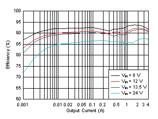
Figure 10-5 LM62440-Q1
Efficiency. Unless otherwise specified, the following conditions apply: VIN
= 13.5 V, TA = 25°C. The circuit is shown in Figure 10-1, with
the appropriate BOM from Table 10-5.

| VOUT = 3.3 V | FSW = 2100 kHz | Auto mode |
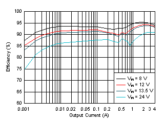
| VOUT = 5 V | FSW = 2100 kHz | Auto mode |
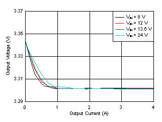
| VOUT = 3.3 V | FSW = 2100 kHz | Auto Mode |
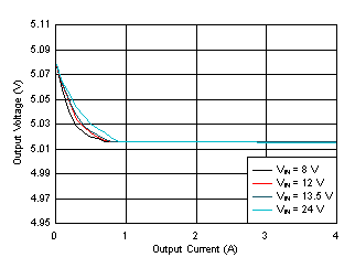
| VOUT = 5V | FSW = 2100 kHz | Auto Mode |
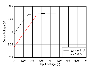
| VOUT = 3.3 V | FSW = 2100 kHz | Auto mode |
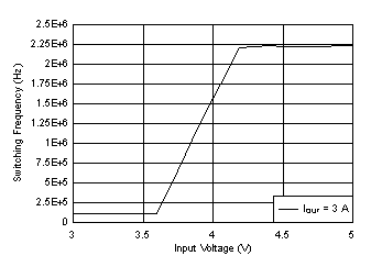
| VOUT = 3.3 V | FSW = 2100 kHz | Auto mode |
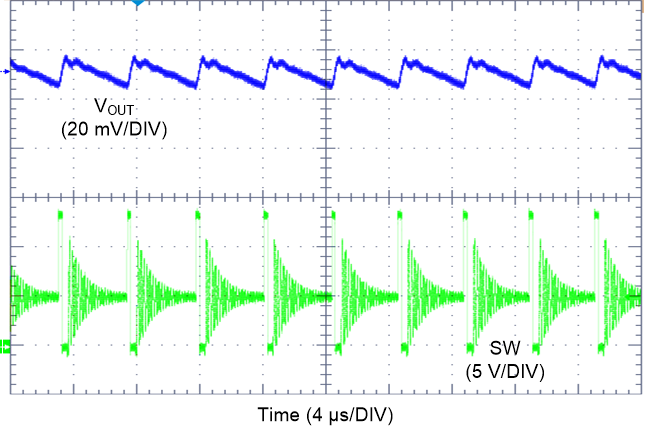
| VOUT = 5 V | FSW = 2100 kHz | Auto mode |
| IOUT = 100 mA | VIN = 13.5 V |
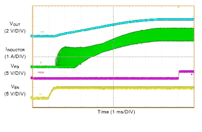
| VOUT = 3.3 V | FSW = 2100 kHz | FPWM mode |
| IOUT = 3.25 A | VIN = 13.5 V |
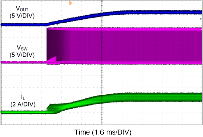
| VOUT = 5 V | FSW = 2100 kHz | FPWM mode |
| IOUT = Short Circuit to 2.5 A | VIN = 13.5 V | |
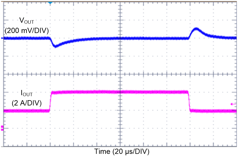
| VOUT = 3.3 V | FSW = 400 kHz | Auto mode |
| IOUT = 2 A to 4 A to 2 A | VIN = 13.5 V | TR = TF = 2µs |
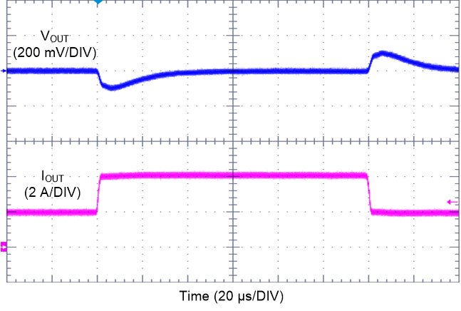
| VOUT = 5 V | FSW = 2100 kHz | Auto mode |
| IOUT = 2 A to 4 A to 2 A | VIN = 13.5 V | TR = TF = 2µs |
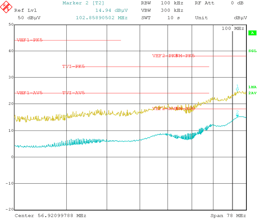
| VOUT = 5 V | FSW = 400 kHz | IOUT = 5 A |
| Frequency Tested: 30 MHz to 108 MHz | ||
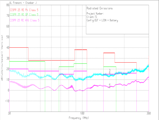
| VOUT = 5 V | FSW = 400 kHz | IOUT = 5 A |
| Frequency Tested: 30 MHz to 300 MHz | ||
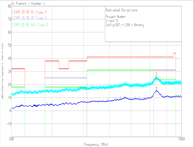
| VOUT = 5 V | FSW = 400 kHz | IOUT = 5 A |
| Frequency Tested: 300 MHz to 1 GHz | ||
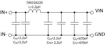
| FSW = 400 kHz | Note: Measurements taken with LM61460EVM with 6 A variant | |
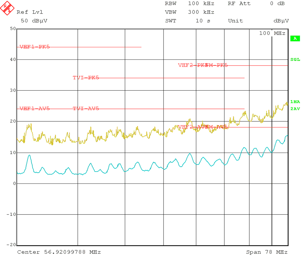
| FSW = 2100 kHz | VOUT = 5 V | IOUT = 5 A |
| Frequency Tested: 30 MHz to 108 MHz | ||
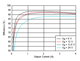
| VOUT = 3.3 V | FSW = 2100 kHz | FPWM mode |
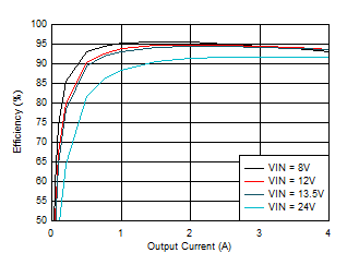
| VOUT = 5 V | FSW = 2100 kHz | FPWM mode |
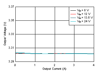
| VOUT = 3.3 V | FSW = 2100 kHz | FPWM mode |
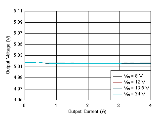
| VOUT = 5V | FSW = 2100 kHz | FPWM mode |
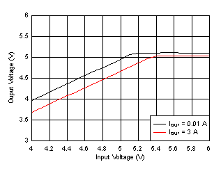
| VOUT = 5 V | FSW = 2100 kHz | Auto mode |
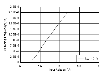
| VOUT = 5 V | FSW = 2100 kHz | Auto mode |
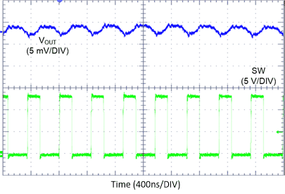
| VOUT = 5 V | FSW = 2100 kHz | Auto mode |
| IOUT = 4 A | VIN = 13.5 V |
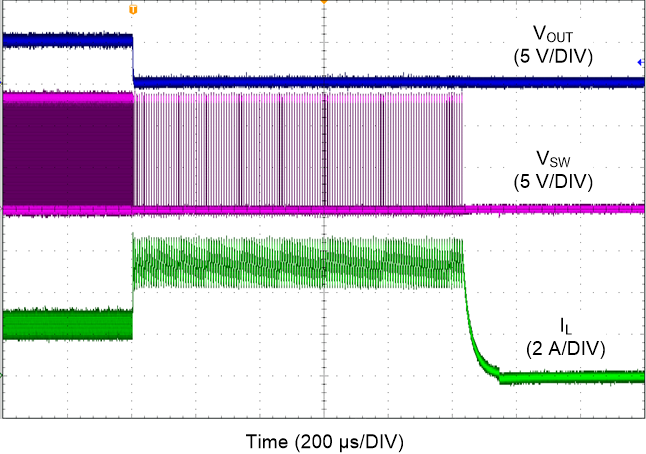
| VOUT = 5 V | FSW = 2100 kHz | FPWM mode |
| IOUT = 2.5 A to Short Circuit | VIN = 13.5 V | |
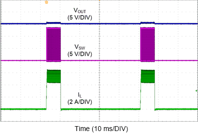
| VOUT = 5 V | FSW = 2100 kHz | FPWM mode |
| IOUT = Short Circuit | VIN = 13.5 V | |
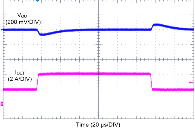
| VOUT = 3.3 V | FSW = 2100 kHz | Auto mode |
| IOUT = 2 A to 4 A to 2 A | VIN = 13.5 V | TR = TF = 2µs |
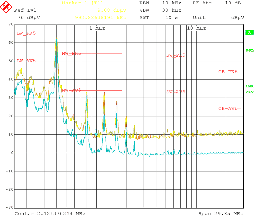
| VOUT = 5 V | FSW = 400 kHz | IOUT = 5 A* |
| Frequency Tested: 150 kHz to 30 MHz | ||
| *Tested on 6 A Variant | ||
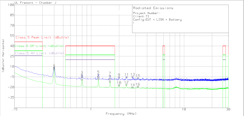
| VOUT = 5 V | FSW = 400 kHz | IOUT = 5 A |
| Frequency Tested: 150 kHz to 30 MHz | ||

| VOUT = 5 V | FSW = 400 kHz | IOUT = 5 A |
| Frequency Tested: 30 MHz to 300 MHz | ||
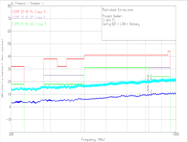
| VOUT = 5 V | FSW = 400 kHz | IOUT = 5 A |
| Frequency Tested: 300 MHz to 1 GHz | ||
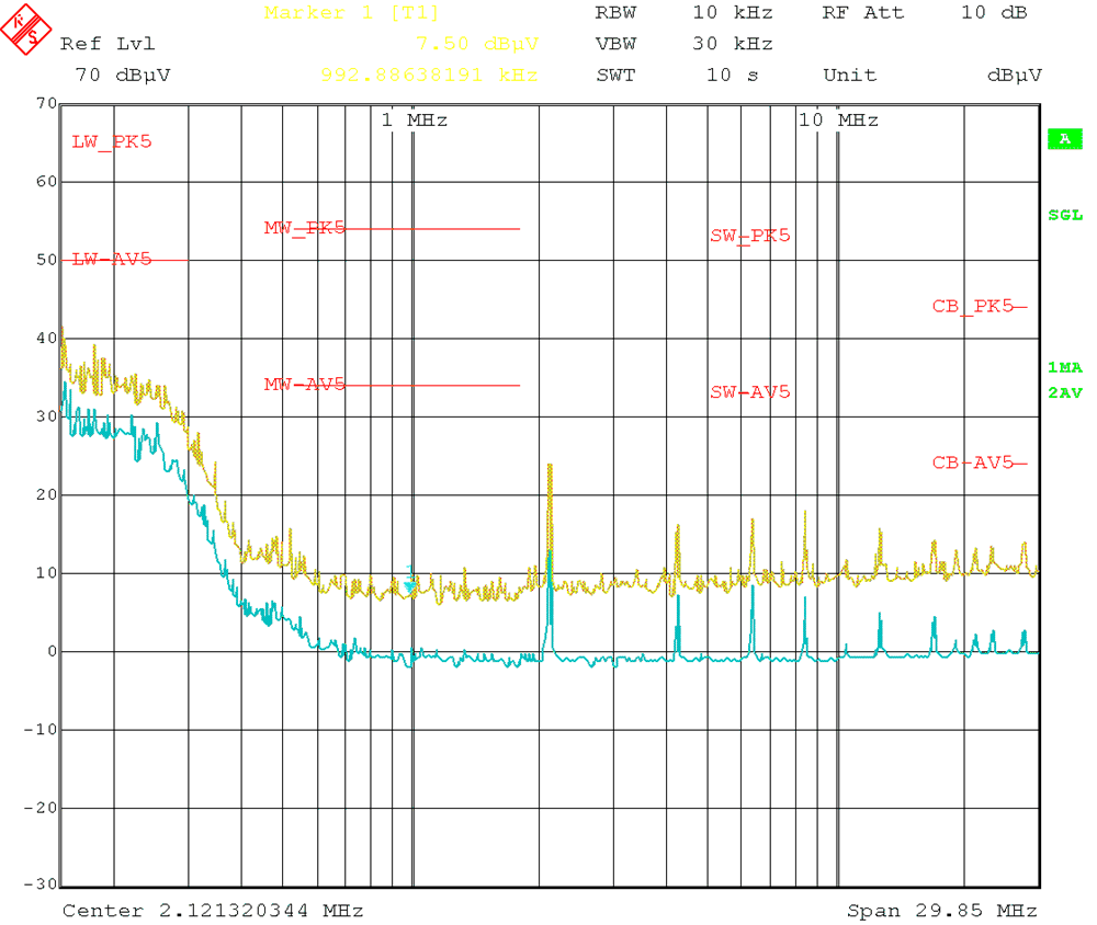
| FSW = 2100 kHz | VOUT = 5 V | IOUT = 5 A* |
| Frequency Tested: 150 kHz to 30 MHz | ||
| *Tested on 6 A Variant | ||
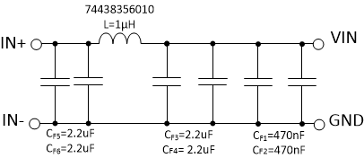
| Note: All EMI measurements taken with 6-A Variant | ||
| FSW = 2100 kHz | ||
Table 10-5 BOM for Typical Application
Curves
| VOUT | Frequency | RFBB | RT | COUT | CIN + CHF | L | CFF |
|---|---|---|---|---|---|---|---|
| 3.3 V | 2100 kHz | 43.2 kΩ | 6.04 kΩ | 3 × 22 µF | 2 × 4.7 µF + 2 × 100 nF | 1.5 µH (MAPI 4020HT) | 22 pF |
| 5 V | 2100 kHz | 24.9 kΩ | 6.04 kΩ | 2 × 22 µF | 2 × 4.7 µF + 2 × 100 nF | 1.5 µH (MAPI 4020HT) | 22 pF |