JAJSIW6E March 2020 – April 2022 LM62440-Q1
PRODUCTION DATA
- 1 特長
- 2 アプリケーション
- 3 概要
- 4 Revision History
- 5 概要 (続き)
- 6 Device Comparison Table
- 7 Pin Configuration and Functions
- 8 Specifications
-
9 Detailed Description
- 9.1 Overview
- 9.2 Functional Block Diagram
- 9.3
Feature Description
- 9.3.1 EN Uses for Enable and VIN UVLO
- 9.3.2 MODE/SYNC Pin Operation
- 9.3.3 PGOOD Output Operation
- 9.3.4 Internal LDO, VCC UVLO, and BIAS Input
- 9.3.5 Bootstrap Voltage and VCBOOT-UVLO (CBOOT Pin)
- 9.3.6 Adjustable SW Node Slew Rate
- 9.3.7 Spread Spectrum
- 9.3.8 Soft Start and Recovery From Dropout
- 9.3.9 Output Voltage Setting
- 9.3.10 Overcurrent and Short Circuit Protection
- 9.3.11 Thermal Shutdown
- 9.3.12 Input Supply Current
- 9.4 Device Functional Modes
-
10Application and Implementation
- 10.1 Application Information
- 10.2
Typical Application
- 10.2.1 Design Requirements
- 10.2.2
Detailed Design Procedure
- 10.2.2.1 Choosing the Switching Frequency
- 10.2.2.2 Setting the Output Voltage
- 10.2.2.3 Inductor Selection
- 10.2.2.4 Output Capacitor Selection
- 10.2.2.5 Input Capacitor Selection
- 10.2.2.6 BOOT Capacitor
- 10.2.2.7 BOOT Resistor
- 10.2.2.8 VCC
- 10.2.2.9 BIAS
- 10.2.2.10 CFF and RFF Selection
- 10.2.2.11 External UVLO
- 10.2.3 Application Curves
- 11Power Supply Recommendations
- 12Layout
- 13Device and Documentation Support
- 14Mechanical, Packaging, and Orderable Information
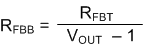
9.3.9 Output Voltage Setting
If the LM62440-Q1 has fixed 5-V or fixed 3.3-V output, simply connect FB to output. See Section 10 for layout information.
For versions of the LM62440-Q1 with adjustable output voltage, a feedback resistor divider network between the output voltage and the FB pin is used to set output voltage level. See Figure 9-17.
 Figure 9-17 Setting Output Voltage of Adjustable Versions
Adjustable versions of the LM62440-Q1 use a 1-V reference voltage for the feedback (FB) pin. The FB pin voltage is regulated by the internal controller to be the same as the reference voltage. The output voltage level is then set by the ratio of the resistor divider. Equation 2 can be used to determine RFBB for a desired output voltage and a given RFBT. Usually RFBT is between 10 kΩ and 1 MΩ. 100 kΩ is recommended for RFBT for improved noise immunity compared to 1 MΩ and reduced current consumption compared to lower resistance values.
In addition, a feedforward capacitor, CFF, connected in parallel with RFBT can be required to optimize the transient response.