SNAS642A June 2014 – July 2014 LMK00804B
PRODUCTION DATA.
- 1 Features
- 2 Applications
- 3 Description
- 4 Simplified Schematic
- 5 Device Comparison Table
- 6 Pin Configuration and Functions
-
7 Specifications
- 7.1 Pin Characteristics
- 7.2 Absolute Maximum Ratings
- 7.3 Handling Ratings
- 7.4 Recommended Operating Conditions
- 7.5 Thermal Information
- 7.6 Power Supply Characteristics
- 7.7 LVCMOS / LVTTL DC Characteristics
- 7.8 Differential Input DC Characteristics
- 7.9 Electrical Characteristics (VDDO = 3.3 V ± 5%)
- 7.10 Electrical Characteristics (VDDO = 2.5 V ± 5%)
- 7.11 Electrical Characteristics (VDDO = 1.8 V ± 0.15 V)
- 7.12 Electrical Characteristics (VDDO = 1.5 V ± 5%)
- 7.13 Typical Characteristics
- 8 Parameter Measurement Information
- 9 Detailed Description
- 10Applications and Implementation
- 11Power Supply Recommendations
- 12Layout
- 13Device and Documentation Support
- 14Mechanical, Packaging, and Orderable Information
10 Applications and Implementation
10.1 Application Information
Refer to the following sections for output clock and input clock interface circuits.
10.2 Output Clock Interface Circuit
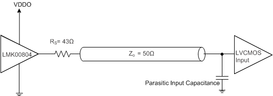 Figure 9. LVCMOS Output Configuration
10.3 Input Detail
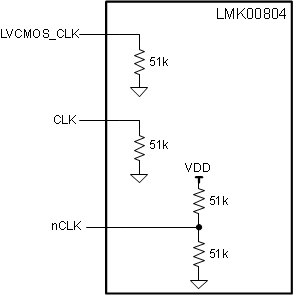 Figure 10. Clock Input Components
10.4 Input Clock Interface Circuits
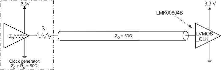 Figure 11. LVCMOS_CLK Input Configuration
10.5 Typical Applications
10.5.1 Design Requirements
For high-performance devices, limitations of the equipment influence phase-noise measurements. The noise floor of the equipment is often higher than the noise floor of the device. The real noise floor of the device is probably lower. It is important to understand that system-level phase noise measured at the DUT output is influenced by the input source and the measurement equipment.
For Figure 18 and Figure 19 system-level phase noise plots, a Rohde & Schwarz SMA100A low-noise signal generator was cascaded with an Agilent 70429A K95 single-ended to differential converter block with ultra-low phase noise and fast edge slew rate (>3 V/ns) to provide a very low-noise clock input source to the LMK00804B. An Agilent E5052 source signal analyzer with ultra-low measurement noise floor was used to measure the phase noise of the input source (SMA100A + 70429A K95) and system output (input source + LMK00804B). The input source phase noise is shown by the light yellow trace, and the system output phase noise is shown by the dark yellow trace.
10.5.2 Detailed Design Procedure
The additive phase noise or noise floor of the buffer (PNFLOOR) can be computed as follows:
where
- PNSYSTEM is the phase noise of the system output (source+buffer)
- PNSOURCE is the phase noise of the input source
The additive jitter of the buffer (JADD) can be computed as follows:
where
- JSYSTEM is the RMS jitter of the system output (source+buffer), integrated from 10 kHz to 20 MHz
- JSOURCE is the RMS jitter of the input source, integrated from 10 kHz to 20 MHz
10.5.3 Application Curves
10.5.3.1 System-Level Phase Noise and Additive Jitter Measurement
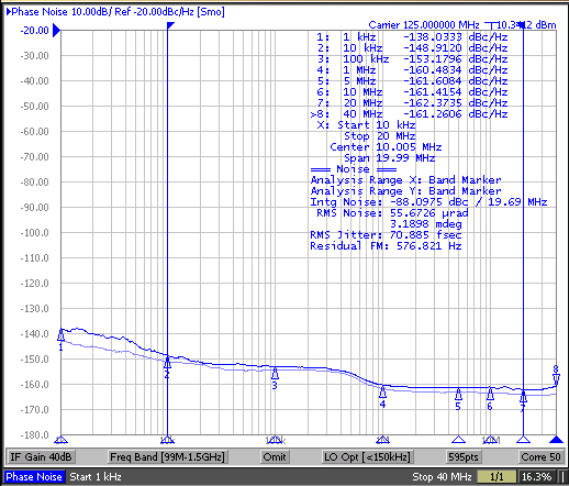 Figure 18.
 125 MHz Input Phase Noise (57 fs rms, Light Blue),
and Output Phase Noise (71 fs rms, Dark Blue),
Additive Jitter = 42 fs rms
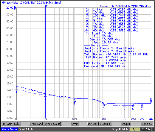 Figure 19.
 156.25 MHz Input Phase Noise (57 fs rms, Light Blue),
and Output Phase Noise (72 fs rms, Dark Blue),
Additive Jitter = 44 fs rms
10.6 Do's and Don'ts
10.6.1 Power Considerations
The following power consideration refers to the device-consumed power consumption only. The device power consumption is the sum of static power and dynamic power. The dynamic power usage consists of two components:
- Power used by the device as it switches states
- Power required to charge any output load
The output load can be capacitive-only or capacitive and resistive. Use the following formula to calculate the power consumption of the device:
where
- IDDO,dyn = CPD × VDDO × f × n [mA]
- IDDO,Cload = Cload × VDDO × f × n [mA]
Example for power consumption of the LMK00804B: 4 outputs are switching, f = 100 MHz,
VDD = VDDO = 3.465 V and assuming Cload = 5 pF per output:
NOTE
For dimensioning the power supply, consider the total power consumption. The total power consumption is the sum of device power consumption and the power consumption of the load.
10.6.2 Recommendations for Unused Input and Output Pins
- CLK_SEL, CLK_EN, and OE: These inputs all have internal pull-up (RPU) according to Table 2 and can be left floating if unused. Table 2 shows the default floating state of these inputs:
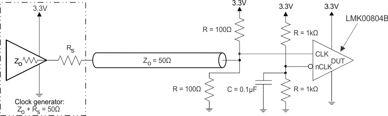
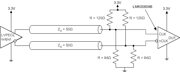
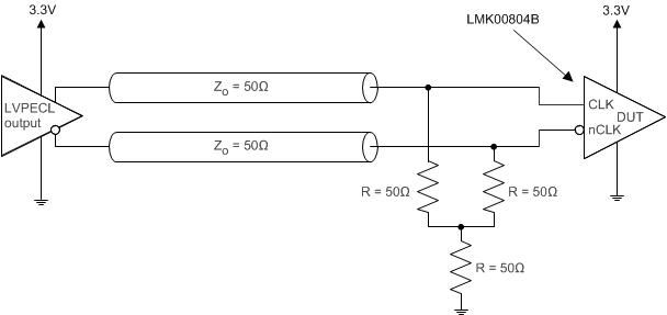
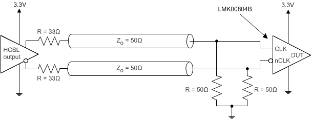
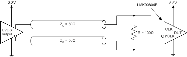
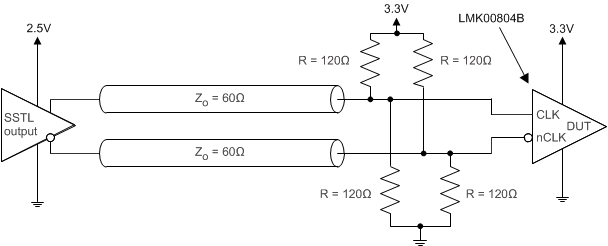
- CLK/nCLK Inputs: See Figure 10 for the internal connections. When using single ended input, take note of the internal pull-up and pull-down to make sure the unused input is properly biased. To interface a single-ended input to the CLK/nCLK input, the configuration shown in Figure 12 is recommended.
- LVCMOS_CLK Input: See Figure 10 for the internal connection. The internal pull-down (RPD) resistor ensures a low state when this input is left floating.
- Outputs: Any unused output can be left floating with no trace connected.
Table 2. Input Floating Default States
| INPUT | FLOATING STATE SELECTION |
|---|---|
| CLK_SEL | CLK/nCLK selected |
| CLK_EN | Synchronous outputs enable |
| OE | Outputs enabled |
10.6.3 Input Slew Rate Considerations
LMK00804B employs high-speed and low-latency circuit topology, allowing the device to achieve ultra-low additive jitter/phase noise and high-frequency operation. To take advantage of these benefits in the system application, it is optimal for the input signal to have a high slew rate of 3 V/ns or greater. Driving the input with a slower slew rate can degrade the additive jitter and noise floor performance. For this reason, a differential signal input is recommended over single-ended because it typically provides higher slew rate and common-mode-rejection. Refer to the “Additive Jitter vs. Input Slew Rate” plots in Typical Characteristics. Also, using an input signal with very slow input slew rate, such as less than 0.05 V/ns, has the tendency to cause output switching noise to feed-back to the input stage and cause the output to chatter. This is especially true when driving either input in single-ended fashion with a very slow slew rate, such as a sine-wave input signal.