SNAS642A June 2014 – July 2014 LMK00804B
PRODUCTION DATA.
- 1 Features
- 2 Applications
- 3 Description
- 4 Simplified Schematic
- 5 Device Comparison Table
- 6 Pin Configuration and Functions
-
7 Specifications
- 7.1 Pin Characteristics
- 7.2 Absolute Maximum Ratings
- 7.3 Handling Ratings
- 7.4 Recommended Operating Conditions
- 7.5 Thermal Information
- 7.6 Power Supply Characteristics
- 7.7 LVCMOS / LVTTL DC Characteristics
- 7.8 Differential Input DC Characteristics
- 7.9 Electrical Characteristics (VDDO = 3.3 V ± 5%)
- 7.10 Electrical Characteristics (VDDO = 2.5 V ± 5%)
- 7.11 Electrical Characteristics (VDDO = 1.8 V ± 0.15 V)
- 7.12 Electrical Characteristics (VDDO = 1.5 V ± 5%)
- 7.13 Typical Characteristics
- 8 Parameter Measurement Information
- 9 Detailed Description
- 10Applications and Implementation
- 11Power Supply Recommendations
- 12Layout
- 13Device and Documentation Support
- 14Mechanical, Packaging, and Orderable Information
7 Specifications
7.1 Pin Characteristics
| MIN | TYP | MAX | UNIT | |||
|---|---|---|---|---|---|---|
| CIN | Input Capacitance | 1 | pF | |||
| RPU | Input Pullup Resistance | 51 | kΩ | |||
| RPD | Input Pulldown Resistance | 51 | kΩ | |||
| CPD | Power Dissipation Capacitance (per output) | 2 | pF | |||
| ROUT | Output impedance | 7 | Ω | |||
7.2 Absolute Maximum Ratings(1)(2)
Over operating free-air temperature range (unless otherwise noted)| MIN | TYP | MAX | UNIT | |||
|---|---|---|---|---|---|---|
| VDD | Core Supply Voltage | –0.3 | 3.6 | V | ||
| VDDO | Output Supply Voltage | –0.3 | 3.6 | V | ||
| VIN | Input Voltage Range | –0.3 | VDD +0.3 |
V | ||
| TJ | Junction Temperature | 150 | °C | |||
(1) Stresses beyond those listed under Absolute Maximum Ratings may cause permanent damage to the device. These are stress ratings only, and functional operation of the device at these or any other conditions beyond those indicated under Recommended Operating Conditions is not implied. Exposure to absolute-maximum-rated conditions for extended periods may affect device reliability.
(2) If Military/Aerospace specified devices are required, please contact the Texas Instruments Sales Office/Distributors for availability and specifications.
7.3 Handling Ratings
| MIN | MAX | UNIT | |||
|---|---|---|---|---|---|
| Tstg | Storage temperature range | –65 | 150 | °C | |
| V(ESD) | Electrostatic discharge(3) | Human body model (HBM), per ANSI/ESDA/JEDEC JS-001, all pins(1) | 1000 | V | |
| Charged device model (CDM), per JEDEC specification JESD22-C101, all pins(2) | 250 | ||||
(1) JEDEC document JEP155 states that 500-V HBM allows safe manufacturing with a standard ESD control process.
(2) JEDEC document JEP157 states that 250-V CDM allows safe manufacturing with a standard ESD control process.
(3) Electrostatic discharge (ESD) to measure device sensitivity and immunity to damage caused by assembly line electrostatic discharges in to the device.
7.4 Recommended Operating Conditions
Over operating free-air temperature range (unless otherwise noted)| MIN | TYP | MAX | UNIT | ||||
|---|---|---|---|---|---|---|---|
| VDD | Core Supply Voltage | 3.135 | 3.3 | 3.465 | V | ||
| VDDO | Output Supply Voltage | 3.135 | 3.3 | 3.465 | V | ||
| 2.375 | 2.5 | 2.625 | |||||
| 1.65 | 1.8 | 1.95 | |||||
| 1.425 | 1.5 | 1.575 | |||||
| TA | Ambient Temperature | -40 | 85 | °C | |||
| TJ | Junction Temperature | 125 | °C | ||||
7.5 Thermal Information
Over operating free-air temperature range (unless otherwise noted)| THERMAL METRIC(1) | MIN | TYP | MAX | UNIT | ||
|---|---|---|---|---|---|---|
| R θJA | Package Thermal Impedance, Junction to Air (0 LFPM) | 116 | °C/W | |||
(1) For more information about traditional and new thermal metrics, see the IC Package Thermal Metrics application report, SPRA953.
7.6 Power Supply Characteristics
Over operating free-air temperature range (unless otherwise noted)| PARAMETER | MIN | TYP | MAX | UNIT | |||
|---|---|---|---|---|---|---|---|
| IDD | Power Supply Current through VDD | 21 | mA | ||||
| IDDO | Power Supply Current through VDDO | 5 | mA | ||||
7.7 LVCMOS / LVTTL DC Characteristics
Over operating free-air temperature range (unless otherwise noted)| PARAMETER | TEST CONDITIONS | MIN | TYP | MAX | UNIT | ||
|---|---|---|---|---|---|---|---|
| VIH | Input High Voltage | CLK_EN, CLK_SEL, OE |
2 | VDD + 0.3 | V | ||
| LVCMOS_CLK | 2 | VDD + 0.3 | V | ||||
| VIL | Input Low Voltage | CLK_EN, CLK_SEL, OE |
–0.3 | 0.8 | V | ||
| LVCMOS_CLK | –0.3 | 1.3 | |||||
| IIH | Input High Current | CLK_EN, CLK_SEL, OE |
VDD = 3.465 V, VIN = 3.465 V |
5 | µA | ||
| LVCMOS_CLK | VDD = 3.465 V, VIN = 3.465 V |
150 | |||||
| IIL | Input Low Current | CLK_EN, CLK_SEL, OE |
VDD = 3.465 V, VIN = 0 V |
–150 | µA | ||
| LVCMOS_CLK | VDD = 3.465 V, VIN = 0 V |
–5 | |||||
| VOH | Output High Voltage(1) | VDDO = 3.3 V ± 5% | 2.6 | V | |||
| VDDO = 2.5 V ± 5% | 1.8 | ||||||
| VDDO = 1.8 V ± 0.15 V | 1.5 | ||||||
| VDDO = 1.5 V ± 5% | VDDO – 0.3 | ||||||
| VOL | Output Low Voltage(1) | VDDO = 3.3 V ± 5% | 0.5 | V | |||
| VDDO = 2.5 V ± 5% | 0.5 | ||||||
| VDDO = 1.8 V ± 0.15 V | 0.4 | ||||||
| VDDO = 1.5 V ± 5% | 0.35 | ||||||
| IOZL | Output Hi-Z Current Low | –5 | µA | ||||
| IOZH | Output Hi-Z Current High | 5 | |||||
(1) Outputs terminated with 50 Ω to VDDO/2.
7.8 Differential Input DC Characteristics
Over operating free-air temperature range (unless otherwise noted)| PARAMETER | TEST CONDITIONS | MIN | TYP | MAX | UNIT | ||
|---|---|---|---|---|---|---|---|
| VID | Differential Input Voltage Swing, (VIH-VIL)(1) |
0.15 | 1.3 | V | |||
| VICM | Input Common Mode Voltage(1)(2) | 0.5 | VDD – 0.85 | V | |||
| IIH | Input High Current(3) | nCLK | VDD = 3.465 V, VIN = 3.465 V |
150 | µA | ||
| CLK | VDD = 3.465 V, VIN = 3.465 V |
150 | |||||
| IIL | Input Low Current(3) | nCLK | VDD = 3.465 V , VIN = 0 V |
-150 | µA | ||
| CLK | VDD = 3.465 V, VIN = 0 V |
-5 | |||||
(1) VIL should not be less than -0.3 V.
(2) Input common mode voltage is defined as VIH.
(3) For IIH and IIL measurements on CLK or nCLK, one must comply with VID and VICM specifications by using the appropriate bias on nCLK or CLK.
7.9 Electrical Characteristics (VDDO = 3.3 V ± 5%)
Over recommended operating free-air temperature range (unless otherwise noted), VDD = VDDO = 3.3V ± 5%,All AC parameters measured at ≤ 350 MHz unless otherwise noted.
| PARAMETER | TEST CONDITIONS | MIN | TYP | MAX | UNIT | ||
|---|---|---|---|---|---|---|---|
| fOUT | Maximum Output Frequency(11)(1) | 350 | MHz | ||||
| tPDLH | Propagation Delay, Low to High(9) |
LVCMOS_CLK(2), CLK/nCLK(3) |
0°C to 70°C | 1.1 | 2.1 | ns | |
| –40°C to 85°C | 0.95 | 2.2 | ns | ||||
| tSK(O) | Output Skew(1)(4)(5) | Measured on rising edge | 35 | ps | |||
| tSK(PP) | Part-to-Part Skew(9)(5)(6) | 700 | ps | ||||
| tR/tF | Output Rise/Fall Time(9) | 20% to 80% | 50 | 700 | ps | ||
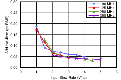
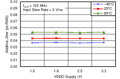
| JADD | Additive Jitter(7) | f=125 MHz, Input slew rate ≥ 3 V/ns, 12 kHz to 20 MHz integration band |
0.04 | ps RMS | |||
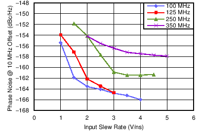
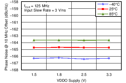
| PNFLOOR | Phase Noise Floor(8) | f = 125 MHz, Input slew rate ≥ 3 V/ns |
dBc/Hz | ||||
| 10 kHz offset | -155 | ||||||
| 100 kHz offset | -162 | ||||||
| 1 MHz offset | -166 | ||||||
| 10 MHz offset | -166 | ||||||
| 20 MHz offset | -166 | ||||||
| ODC | Output Duty Cycle(9)(10) | REF = CLK/nCLK | 45% | 55% | |||
| REF = LVCMOS_CLK, f ≤ 300 MHz |
45% | 55% | |||||
| tEN | Output Enable Time | 5 | ns | ||||
| tDIS | Output Disable Time | 5 | ns | ||||
(1) These AC parameters are specified by characterization. Not tested in production.
(2) Measured from the VDD/2 of the input to the VDDO/2 of the output.
(3) Measured from the differential input crossing point to VDDO/2 of the output.
(4) Defined as skew between outputs at the same supply voltage and with equal loading conditions. Measured at VDDO/2 of the output.
(5) Parameter is defined in accordance with JEDEC Standard 65.
(6) Calculation for part-to-part skew is the difference between the fastest and slowest tPD across multiple devices, operating at the same supply voltage, same frequency, same temperature, with equal load conditions, and using the same type of inputs on each device.
(7) Buffer Additive Jitter: JADD = SQRT(JSYSTEM 2 - JSOURCE2), where JSYSTEM is the RMS jitter of the system output (source+buffer) and JSOURCE is the RMS jitter of the input source, and system output noise is not correlated to the input source noise. Additive jitter should be considered only when the input source noise floor is 3 dB or better than the buffer noise floor (PNFLOOR). This is usually the case for high-quality ultra-low-noise oscillators. Please refer to System-Level Phase Noise and Additive Jitter Measurement for input source and measurement details.
(8) Buffer Phase Noise Floor: PNFLOOR (dBc/Hz) = 10 x log10[10^(PNSYSTEM/10) – 10^(PNSOURCE/10)], where PNSYSTEM is the phase noise floor of the system output (source+buffer) and PNSOURCE is the phase noise floor of the input source. Buffer Phase Noise Floor should be considered only when the input source noise floor is 3 dB or better than the buffer noise floor (PNFLOOR). This is usually the case for high-quality ultra-low-noise oscillators. Please refer to System-Level Phase Noise and Additive Jitter Measurement for input source and measurement details.
(9) These AC parameters are specified by design. Not tested in production
(10) 50% Input duty cycle
(11) There is no minimum input / output frequency provided the input slew rate is sufficiently fast. Refer to Input Slew Rate Considerations.
7.10 Electrical Characteristics (VDDO = 2.5 V ± 5%)
Over recommended operating free-air temperature range (unless otherwise noted), VDD = 3.3V ± 5%, VDDO = 2.5V ± 5%,All AC parameters measured at ≤ 350 MHz unless otherwise noted.
| PARAMETER | TEST CONDITIONS | MIN | TYP | MAX | UNIT | ||
|---|---|---|---|---|---|---|---|
| fOUT | Maximum Output Frequency(10)(1) | 350 | MHz | ||||
| tPDLH | Propagation Delay, Low to High(8) |
LVCMOS_CLK(2), CLK/nCLK(3) |
0°C to 70°C | 1.1 | 2.1 | ns | |
| –40°C to 85°C | 0.95 | 2.2 | |||||
| tSK(O) | Output Skew(1)(4)(5) | Measured on rising edge | 35 | ps | |||
| tSK(PP) | Part-to-Part Skew(8)(5)(6) | 700 | ps | ||||
| tR/tF | Output Rise/Fall Time(8) | 20% to 80% | 50 | 700 | ps | ||
| JADD | Additive Jitter(7) | f=125 MHz, Input slew rate ≥ 3 V/ns, 12 kHz to 20 MHz integration band |
0.04 | ps RMS | |||
| ODC | Output Duty Cycle(8)(9) | REF = CLK/nCLK | 45% | 55% | |||
| REF = LVCMOS_CLK, f ≤ 300 MHz |
45% | 55% | |||||
| tEN | Output Enable Time | 5 | ns | ||||
| tDIS | Output Disable Time | 5 | ns | ||||
(1) These AC parameters are specified by characterization. Not tested in production.
(2) Measured from the VDD/2 of the input to the VDDO/2 of the output.
(3) Measured from the differential input crossing point to VDDO/2 of the output.
(4) Defined as skew between outputs at the same supply voltage and with equal loading conditions. Measured at VDDO/2 of the output.
(5) Parameter is defined in accordance with JEDEC Standard 65.
(6) Calculation for part-to-part skew is the difference between the fastest and slowest tPD across multiple devices, operating at the same supply voltage, same frequency, same temperature, with equal load conditions, and using the same type of inputs on each device.
(7) Buffer Additive Jitter: JADD = SQRT(JSYSTEM2 - JSOURCE2), where JSYSTEM is the RMS jitter of the system output (source+buffer) and JSOURCE is the RMS jitter of the input source, and system output noise is not correlated to the input source noise. Additive jitter should be considered only when the input source noise floor is 3 dB or better than the buffer noise floor (PNFLOOR). This is usually the case for high-quality ultra-low-noise oscillators. Please refer to System-Level Phase Noise and Additive Jitter Measurement for input source and measurement details.
(8) These AC parameters are specified by design. Not tested in production.
(9) 50% Input Duty Cycle
(10) There is no minimum input / output frequency provided the input slew rate is sufficiently fast. Refer to Input Slew Rate Considerations.
7.11 Electrical Characteristics (VDDO = 1.8 V ± 0.15 V)
Over recommended operating free-air temperature range (unless otherwise noted), VDD = 3.3 V ± 5%,VDDO = 1.8 V ± 0.15 V. All AC parameters measured at ≤ 350 MHz unless otherwise noted.
| PARAMETER | TEST CONDITIONS | MIN | TYP | MAX | UNIT | ||
|---|---|---|---|---|---|---|---|
| fOUT | Maximum Output Frequency(10)(1) | 350 | MHz | ||||
| tPDLH | Propagation Delay, Low to High(8) |
LVCMOS_CLK(2), CLK/nCLK(3) |
0°C to 70°C | 1.1 | 2.2 | ns | |
| –40°C to 85°C | 0.95 | 2.3 | ns | ||||
| tSK(O) | Output Skew(1)(4)(5) | Measured on rising edge | 35 | ps | |||
| tSK(PP) | Part-to-Part Skew(8)(5)(6) | 700 | ps | ||||
| tR/tF | Output Rise/Fall Time(8) | 20% to 80% | 100 | 700 | ps | ||
| JADD | Additive Jitter(7) | f=125 MHz, Input slew rate ≥ 3 V/ns, 12 kHz to 20 MHz integration band |
0.04 | ps RMS | |||
| ODC | Output Duty Cycle(8)(9) | REF = CLK/nCLK | 45% | 55% | |||
| REF = LVCMOS_CLK, f ≤ 300 MHz |
45% | 55% | |||||
| tEN | Output Enable Time | 5 | ns | ||||
| tDIS | Output Disable Time | 5 | ns | ||||
(1) These AC parameters are specified by characterization. Not tested in production.
(2) Measured from the VDD/2 of the input to the VDDO/2 of the output.
(3) Measured from the differential input crossing point to VDDO/2 of the output.
(4) Defined as skew between outputs at the same supply voltage and with equal loading conditions. Measured at VDDO/2 of the output.
(5) Parameter is defined in accordance with JEDEC Standard 65.
(6) Calculation for part-to-part skew is the difference between the fastest and slowest tPD across multiple devices, operating at the same supply voltage, same frequency, same temperature, with equal load conditions, and using the same type of inputs on each device.
(7) Buffer Additive Jitter: JADD = SQRT(JSYSTEM2 - JSOURCE 2), where JSYSTEM is the RMS jitter of the system output (source+buffer) and JSOURCE is the RMS jitter of the input source, and system output noise is not correlated to the input source noise. Additive jitter should be considered only when the input source noise floor is 3 dB or better than the buffer noise floor (PNFLOOR). This is usually the case for high-quality ultra-low-noise oscillators. Please refer to System-Level Phase Noise and Additive Jitter Measurement for input source and measurement details.
(8) These AC parameters are specified by design. Not tested in production.
(9) 50% Input Duty Cycle
(10) There is no minimum input / output frequency provided the input slew rate is sufficiently fast. Refer to Input Slew Rate Considerations.
7.12 Electrical Characteristics (VDDO = 1.5 V ± 5%)
Over recommended operating free-air temperature range (unless otherwise noted), VDD = 3.3V ± 5%, VDDO = 1.5V ± 5%,All AC parameters measured at ≤ 350 MHz unless otherwise noted.
| PARAMETER | TEST CONDITIONS | MIN | TYP | MAX | UNIT | ||
|---|---|---|---|---|---|---|---|
| fOUT | Maximum Output Frequency(10)(1) | 350 | MHz | ||||
| tPDLH | Propagation Delay, Low to High(8) |
LVCMOS_CLK(2), CLK/nCLK(3) |
0°C to 70°C | 1.1 | 2.2 | ns | |
| –40°C to 85°C | 0.95 | 2.3 | ns | ||||
| tSK(O) | Output Skew(1)(4)(5) | Measured on rising edge | 35 | ps | |||
| tSK(PP) | Part-to-Part Skew(1)(5)(6) | 1 | ns | ||||
| tR/tF | Output Rise/Fall Time(8) | 20% to 80% | 100 | 900 | ps | ||
| JADD | Additive Jitter(7) | f=125 MHz, Input slew rate ≥ 3 V/ns, 12 kHz to 20 MHz integration band |
0.04 | ps RMS | |||
| ODC | Output Duty Cycle(8)(9) | f ≤ 166 MHz | 45% | 55% | |||
| f > 166 MHz | 42% | 58% | |||||
| tEN | Output Enable Time | 5 | ns | ||||
| tDIS | Output Disable Time | 5 | ns | ||||
(1) These AC parameters are specified by characterization. Not tested in production.
(2) Measured from the VDD/2 of the input to the VDDO/2 of the output.
(3) Measured from the differential input crossing point to VDDO/2 of the output.
(4) Defined as skew between outputs at the same supply voltage and with equal loading conditions. Measured at VDDO/2 of the output.
(5) Parameter is defined in accordance with JEDEC Standard 65.
(6) Calculation for part-to-part skew is the difference between the fastest and slowest tPD across multiple devices, operating at the same supply voltage, same frequency, same temperature, with equal load conditions, and using the same type of inputs on each device.
(7) Buffer Additive Jitter: JADD = SQRT(JSYSTEM2 - J SOURCE2), where JSYSTEM is the RMS jitter of the system output (source+buffer) and JSOURCE is the RMS jitter of the input source, and system output noise is not correlated to the input source noise. Additive jitter should be considered only when the input source noise floor is 3 dB or better than the buffer noise floor (PNFLOOR). This is usually the case for high-quality ultra-low-noise oscillators. Please refer to System-Level Phase Noise and Additive Jitter Measurement for input source and measurement details.
(8) These AC parameters are specified by design. Not tested in production.
(9) 50% Input Duty Cycle
(10) There is no minimum input / output frequency provided the input slew rate is sufficiently fast. Refer to Input Slew Rate Considerations.
7.13 Typical Characteristics
Unless otherwise noted: VDD = 3.3 V, VDDO = 3.3 V, TA = 25°C