JAJSNL5A October   2022  – November 2022 LMK04832-SEP

PRODUCTION DATA  

  1. 特長
  2. アプリケーション
  3. 概要
  4. Revision History
  5. Pin Configuration and Functions
  6. Specifications
    1. 6.1 Absolute Maximum Ratings
    2. 6.2 ESD Ratings
    3. 6.3 Recommended Operating Conditions
    4. 6.4 Thermal Information
    5. 6.5 Electrical Characteristics
    6. 6.6 Timing Requirements
    7. 6.7 Timing Diagram
    8. 6.8 Typical Characteristics
  7. Parameter Measurement Information
    1. 7.1 Charge Pump Current Specification Definitions
      1. 7.1.1 Charge Pump Output Current Magnitude Variation vs Charge Pump Output Voltage
      2. 7.1.2 Charge Pump Sink Current vs Charge Pump Output Source Current Mismatch
      3. 7.1.3 Charge Pump Output Current Magnitude Variation vs Ambient Temperature
    2. 7.2 Differential Voltage Measurement Terminology
  8. Detailed Description
    1. 8.1 Overview
      1. 8.1.1 Differences from the LMK04832
        1. 8.1.1.1 Jitter Cleaning
        2. 8.1.1.2 JEDEC JESD204B/C Support
      2. 8.1.2 Clock Inputs
        1. 8.1.2.1 Inputs for PLL1
        2. 8.1.2.2 Inputs for PLL2
        3. 8.1.2.3 Inputs When Using Clock Distribution Mode
      3. 8.1.3 PLL1
        1. 8.1.3.1 Frequency Holdover
        2. 8.1.3.2 External VCXO for PLL1
      4. 8.1.4 PLL2
        1. 8.1.4.1 Internal VCOs for PLL2
        2. 8.1.4.2 External VCO Mode
      5. 8.1.5 Clock Distribution
        1. 8.1.5.1 Clock Divider
        2. 8.1.5.2 High Performance Divider Bypass Mode
        3. 8.1.5.3 SYSREF Clock Divider
        4. 8.1.5.4 Device Clock Delay
        5. 8.1.5.5 Dynamic Digital Delay
        6. 8.1.5.6 SYSREF Delay: Global and Local
        7. 8.1.5.7 Programmable Output Formats
        8. 8.1.5.8 Clock Output Synchronization
      6. 8.1.6 0-Delay
      7. 8.1.7 Status Pins
    2. 8.2 Functional Block Diagram
    3. 8.3 Feature Description
      1. 8.3.1 Synchronizing PLL R Dividers
        1. 8.3.1.1 PLL1 R Divider Synchronization
        2. 8.3.1.2 PLL2 R Divider Synchronization
      2. 8.3.2 SYNC/SYSREF
      3. 8.3.3 JEDEC JESD204B/C
        1. 8.3.3.1 How to Enable SYSREF
          1. 8.3.3.1.1 Setup of SYSREF Example
          2. 8.3.3.1.2 SYSREF_CLR
        2. 8.3.3.2 SYSREF Modes
          1. 8.3.3.2.1 SYSREF Pulser
          2. 8.3.3.2.2 Continuous SYSREF
          3. 8.3.3.2.3 SYSREF Request
      4. 8.3.4 Digital Delay
        1. 8.3.4.1 Fixed Digital Delay
          1. 8.3.4.1.1 Fixed Digital Delay Example
        2. 8.3.4.2 Dynamic Digital Delay
        3. 8.3.4.3 Single and Multiple Dynamic Digital Delay Example
      5. 8.3.5 SYSREF to Device Clock Alignment
      6. 8.3.6 Input Clock Switching
        1. 8.3.6.1 Input Clock Switching - Manual Mode
        2. 8.3.6.2 Input Clock Switching - Pin Select Mode
        3. 8.3.6.3 Input Clock Switching - Automatic Mode
      7. 8.3.7 Digital Lock Detect (DLD)
        1. 8.3.7.1 Calculating Digital Lock Detect Frequency Accuracy
      8. 8.3.8 Holdover
        1. 8.3.8.1 Enable Holdover
          1. 8.3.8.1.1 Fixed (Manual) CPout1 Holdover Mode
          2. 8.3.8.1.2 Tracked CPout1 Holdover Mode
        2. 8.3.8.2 During Holdover
        3. 8.3.8.3 Exiting Holdover
        4. 8.3.8.4 Holdover Frequency Accuracy and DAC Performance
      9. 8.3.9 PLL2 Loop Filter
    4. 8.4 Device Functional Modes
      1. 8.4.1 DUAL PLL
        1. 8.4.1.1 Dual Loop
        2. 8.4.1.2 Dual Loop With Cascaded 0-Delay
        3. 8.4.1.3 Dual Loop With Nested 0-Delay
      2. 8.4.2 Single PLL
        1. 8.4.2.1 PLL2 Single Loop
        2. 8.4.2.2 PLL2 With External VCO
      3. 8.4.3 Distribution Mode
    5. 8.5 Programming
      1. 8.5.1 Recommended Programming Sequence
    6. 8.6 Register Maps
      1. 8.6.1 Register Map for Device Programming
      2. 8.6.2 Device Register Descriptions
        1. 8.6.2.1 System Functions
          1. 8.6.2.1.1 RESET, SPI_3WIRE_DIS
          2. 8.6.2.1.2 POWERDOWN
          3. 8.6.2.1.3 ID_DEVICE_TYPE
          4. 8.6.2.1.4 ID_PROD
          5. 8.6.2.1.5 ID_MASKREV
          6. 8.6.2.1.6 ID_VNDR
        2. 8.6.2.2 (0x100 - 0x138) Device Clock and SYSREF Clock Output Controls
          1. 8.6.2.2.1 DCLKX_Y_DIV
          2. 8.6.2.2.2 DCLKX_Y_DDLY
          3. 8.6.2.2.3 CLKoutX_Y_PD, CLKoutX_Y_ODL, CLKoutX_Y_IDL, DCLKX_Y_DDLY_PD, DCLKX_Y_DDLY[9:8], DCLKX_Y_DIV[9:8]
          4. 8.6.2.2.4 CLKoutX_SRC_MUX, DCLKX_Y_PD, DCLKX_Y_BYP, DCLKX_Y_DCC, DCLKX_Y_POL, DCLKX_Y_HS
          5. 8.6.2.2.5 CLKoutY_SRC_MUX, SCLKX_Y_PD, SCLKX_Y_DIS_MODE, SCLKX_Y_POL, SCLKX_Y_HS
          6. 8.6.2.2.6 SCLKX_Y_ADLY_EN, SCLKX_Y_ADLY
          7. 8.6.2.2.7 SCLKX_Y_DDLY
          8. 8.6.2.2.8 CLKoutY_FMT, CLKoutX_FMT
        3. 8.6.2.3 SYSREF, SYNC, and Device Config
          1. 8.6.2.3.1  VCO_MUX, OSCout_MUX, OSCout_FMT
          2. 8.6.2.3.2  SYSREF_REQ_EN, SYNC_BYPASS, SYSREF_MUX
          3. 8.6.2.3.3  SYSREF_DIV
          4. 8.6.2.3.4  SYSREF_DDLY
          5. 8.6.2.3.5  SYSREF_PULSE_CNT
          6. 8.6.2.3.6  PLL2_RCLK_MUX, PLL2_NCLK_MUX, PLL1_NCLK_MUX, FB_MUX, FB_MUX_EN
          7. 8.6.2.3.7  PLL1_PD, VCO_LDO_PD, VCO_PD, OSCin_PD, SYSREF_GBL_PD, SYSREF_PD, SYSREF_DDLY_PD, SYSREF_PLSR_PD
          8. 8.6.2.3.8  DDLYdSYSREF_EN, DDLYdX_EN
          9. 8.6.2.3.9  DDLYd_STEP_CNT
          10. 8.6.2.3.10 SYSREF_CLR, SYNC_1SHOT_EN, SYNC_POL, SYNC_EN, SYNC_PLL2_DLD, SYNC_PLL1_DLD, SYNC_MODE
          11. 8.6.2.3.11 SYNC_DISSYSREF, SYNC_DISX
          12. 8.6.2.3.12 PLL1R_SYNC_EN, PLL1R_SYNC_SRC, PLL2R_SYNC_EN, FIN0_DIV2_EN, FIN0_INPUT_TYPE
        4. 8.6.2.4 (0x146 - 0x149) CLKIN Control
          1. 8.6.2.4.1 CLKin_SEL_PIN_EN, CLKin_SEL_PIN_POL, CLKin2_EN, CLKin1_EN, CLKin0_EN, CLKin2_TYPE, CLKin1_TYPE, CLKin0_TYPE
          2. 8.6.2.4.2 CLKin_SEL_AUTO_REVERT_EN, CLKin_SEL_AUTO_EN, CLKin_SEL_MANUAL, CLKin1_DEMUX, CLKin0_DEMUX
          3. 8.6.2.4.3 CLKin_SEL0_MUX, CLKin_SEL0_TYPE
          4. 8.6.2.4.4 SDIO_RDBK_TYPE, CLKin_SEL1_MUX, CLKin_SEL1_TYPE
        5. 8.6.2.5 RESET_MUX, RESET_TYPE
        6. 8.6.2.6 (0x14B - 0x152) Holdover
          1. 8.6.2.6.1 LOS_TIMEOUT, LOS_EN, TRACK_EN, HOLDOVER_FORCE, MAN_DAC_EN, MAN_DAC[9:8]
          2. 8.6.2.6.2 MAN_DAC
          3. 8.6.2.6.3 DAC_TRIP_LOW
          4. 8.6.2.6.4 DAC_CLK_MULT, DAC_TRIP_HIGH
          5. 8.6.2.6.5 DAC_CLK_CNTR
          6. 8.6.2.6.6 CLKin_OVERRIDE, HOLDOVER_EXIT_MODE, HOLDOVER_PLL1_DET, LOS_EXTERNAL_INPUT, HOLDOVER_VTUNE_DET, CLKin_SWITCH_CP_TRI, HOLDOVER_EN
          7. 8.6.2.6.7 HOLDOVER_DLD_CNT
        7. 8.6.2.7 (0x153 - 0x15F) PLL1 Configuration
          1. 8.6.2.7.1 CLKin0_R
          2. 8.6.2.7.2 CLKin1_R
          3. 8.6.2.7.3 CLKin2_R
          4. 8.6.2.7.4 PLL1_N
          5. 8.6.2.7.5 PLL1_WND_SIZE, PLL1_CP_TRI, PLL1_CP_POL, PLL1_CP_GAIN
          6. 8.6.2.7.6 PLL1_DLD_CNT
          7. 8.6.2.7.7 HOLDOVER_EXIT_NADJ
          8. 8.6.2.7.8 PLL1_LD_MUX, PLL1_LD_TYPE
        8. 8.6.2.8 (0x160 - 0x16E) PLL2 Configuration
          1. 8.6.2.8.1 PLL2_R
          2. 8.6.2.8.2 PLL2_P, OSCin_FREQ, PLL2_REF_2X_EN
          3. 8.6.2.8.3 PLL2_N_CAL
          4. 8.6.2.8.4 PLL2_N
          5. 8.6.2.8.5 PLL2_WND_SIZE, PLL2_CP_GAIN, PLL2_CP_POL, PLL2_CP_TRI
          6. 8.6.2.8.6 PLL2_DLD_CNT
          7. 8.6.2.8.7 PLL2_LD_MUX, PLL2_LD_TYPE
        9. 8.6.2.9 (0x16F - 0x555) Misc Registers
          1. 8.6.2.9.1 PLL2_PRE_PD, PLL2_PD, FIN0_PD
          2. 8.6.2.9.2 PLL1R_RST
          3. 8.6.2.9.3 CLR_PLL1_LD_LOST, CLR_PLL2_LD_LOST
          4. 8.6.2.9.4 RB_PLL1_LD_LOST, RB_PLL1_LD, RB_PLL2_LD_LOST, RB_PLL2_LD
          5. 8.6.2.9.5 RB_DAC_VALUE (MSB), RB_CLKinX_SEL, RB_CLKinX_LOS
          6. 8.6.2.9.6 RB_DAC_VALUE
          7. 8.6.2.9.7 RB_HOLDOVER
          8. 8.6.2.9.8 SPI_LOCK
  9. Application and Implementation
    1. 9.1 Application Information
      1. 9.1.1 Treatment of Unused Pins
      2. 9.1.2 Frequency Planning and Spur Minimization
      3. 9.1.3 Digital Lock Detect Frequency Accuracy
        1. 9.1.3.1 Minimum Lock Time Calculation Example
      4. 9.1.4 Driving CLKIN AND OSCIN Inputs
        1. 9.1.4.1 Driving CLKIN and OSCIN PINS With a Differential Source
        2. 9.1.4.2 Driving CLKIN Pins With a Single-Ended Source
      5. 9.1.5 OSCin Doubler for Best Phase Noise Performance
      6. 9.1.6 Radiation Environments
        1. 9.1.6.1 Total Ionizing Dose
        2. 9.1.6.2 Single Event Effect
    2. 9.2 Typical Application
      1. 9.2.1 Design Requirements
      2. 9.2.2 Detailed Design Procedure
        1. 9.2.2.1 Device Selection
          1. 9.2.2.1.1 Clock Architect
        2. 9.2.2.2 Device Configuration and Simulation
        3. 9.2.2.3 Device Setup
      3. 9.2.3 Application Curve
    3. 9.3 Power Supply Recommendations
      1. 9.3.1 Current Consumption
      2. 9.3.2 Cold Sparing Considerations
        1. 9.3.2.1 Damage Prevention Details to Unpowered Device
    4. 9.4 Layout
      1. 9.4.1 Layout Guidelines
      2. 9.4.2 Layout Example
      3. 9.4.3 Thermal Management
  10. 10Device and Documentation Support
    1. 10.1 Device Support
      1. 10.1.1 Development Support
        1. 10.1.1.1 Clock Architect
        2. 10.1.1.2 PLLatinum Simulation
        3. 10.1.1.3 TICS Pro
    2. 10.2 Documentation Support
      1. 10.2.1 Related Documentation
    3. 10.3 Receiving Notification of Documentation Updates
    4. 10.4 サポート・リソース
    5. 10.5 Trademarks
    6. 10.6 Electrostatic Discharge Caution
    7. 10.7 Glossary
  11. 11Mechanical, Packaging, and Orderable Information

パッケージ・オプション

メカニカル・データ(パッケージ|ピン)
サーマルパッド・メカニカル・データ
発注情報

Digital Lock Detect Frequency Accuracy

The digital lock detect circuit is used to determine PLL1 locked, PLL2 locked, and holdover exit events. A window size and lock count register are programmed to set a ppm frequency accuracy of reference to feedback signals of the PLL for each event to occur. When a PLL digital lock event occurs, the digital lock detect of the PLL is asserted true. When the holdover exit event occurs, the device will exit holdover mode when HOLDOVER_EXIT_MODE = 1 (Exit based on DLD).

Table 9-4 Digital Lock Detect Related Fields
EVENTPLLWINDOW SIZELOCK COUNT
PLL1 LockedPLL1PLL1_WND_SIZEPLL1_DLD_CNT
PLL2 LockedPLL2PLL2_WND_SIZEPLL2_DLD_CNT
Holdover exitPLL1PLL1_WND_SIZEHOLDOVER_DLD_CNT

For a digital lock detect event to occur, there must be a lock count number of phase detector cycles of PLLX during which the time and phase error of the PLLX_R reference and PLLX_N feedback signal edges are within the user programmable window size. There must be at least one lock count phase detector event before a lock event occurs, therefore a minimum digital lock event time can be calculated as lock count / fPDX where X = 1 for PLL1 or 2 for PLL2.

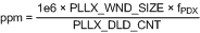
By using Equation 4, values for a lock count and window size can be chosen to set the frequency accuracy required by the system in ppm before the digital lock detect event occurs:

Equation 4. GUID-077E5DD0-0DD4-4D2D-B0E6-AF699A4C7309-low.gif

The effect of the lock count value is that it shortens the effective lock window size by dividing the window size by lock count.

If at any time the PLLX_R reference and PLLX_N feedback signals are outside the time window set by window size, then the lock count value is reset to 0.