JAJSHL7F October   2011  – June 2019 LMR24220

PRODUCTION DATA.  

  1. 1 特長
  2. 2 アプリケーション
  3. 3 概要
    1.     Device Images
      1.      代表的なアプリケーション
  4. 4 改訂履歴
  5. 5 Pin Configuration and Functions
    1.     Pin Descriptions
  6. 6 Specifications
    1. 6.1 Absolute Maximum Ratings
    2. 6.2 Recommended Operating Ratings
    3. 6.3 Electrical Characteristics
    4. 6.4 Typical Characteristics
  7. 7 Detailed Description
    1. 7.1 Overview
    2. 7.2 Functional Block Diagram
    3. 7.3 Feature Description
      1. 7.3.1  CoT Control Circuit Overview
      2. 7.3.2  Start-up Regulator (VCC)
      3. 7.3.3  Regulation Comparator
      4. 7.3.4  Zero Coil Current Detect
      5. 7.3.5  Overvoltage Comparator
      6. 7.3.6  On-Time Timer, Shutdown
      7. 7.3.7  Current Limit
      8. 7.3.8  N-Channel MOSFET and Driver
      9. 7.3.9  Soft Start
      10. 7.3.10 Thermal Protection
  8. 8 Application and Implementation
    1. 8.1 Application Information
    2. 8.2 Typical Application
      1. 8.2.1 Detailed Design Procedure
        1. 8.2.1.1 Custom Design With WEBENCH® Tools
        2. 8.2.1.2 External Components
      2. 8.2.2 Application Curve
  9. 9 Layout
    1. 9.1 Layout Guidelines
    2. 9.2 Package Considerations
    3. 9.3 Thermal Derating
  10. 10デバイスおよびドキュメントのサポート
    1. 10.1 デバイス・サポート
      1. 10.1.1 開発サポート
        1. 10.1.1.1 WEBENCH®ツールによるカスタム設計
    2. 10.2 ドキュメントの更新通知を受け取る方法
    3. 10.3 コミュニティ・リソース
    4. 10.4 商標
    5. 10.5 静電気放電に関する注意事項
    6. 10.6 Glossary
  11. 11メカニカル、パッケージ、および注文情報

パッケージ・オプション

メカニカル・データ(パッケージ|ピン)
サーマルパッド・メカニカル・データ
発注情報

Typical Characteristics

Unless otherwise specified all curves are taken at VIN = 18 V with the configuration in the typical application circuit for
VOUT = 3.3 V (Figure 25) TA = 25°C.
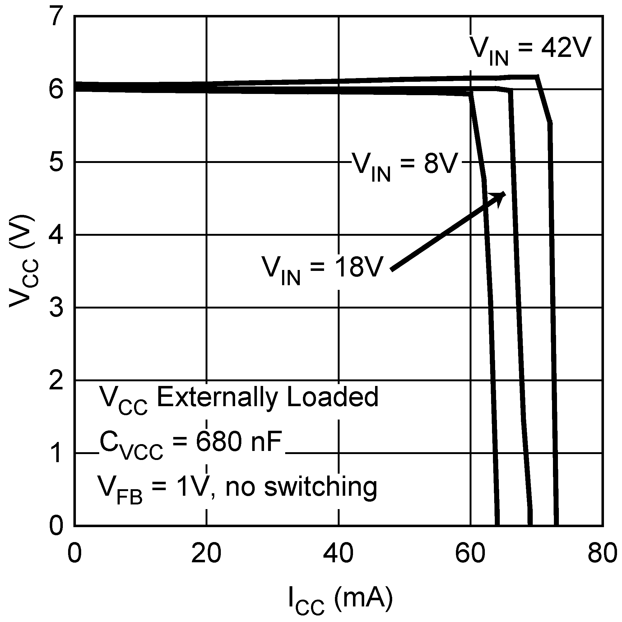
LMR24220 30167604.png
Figure 1. VCC vs ICC
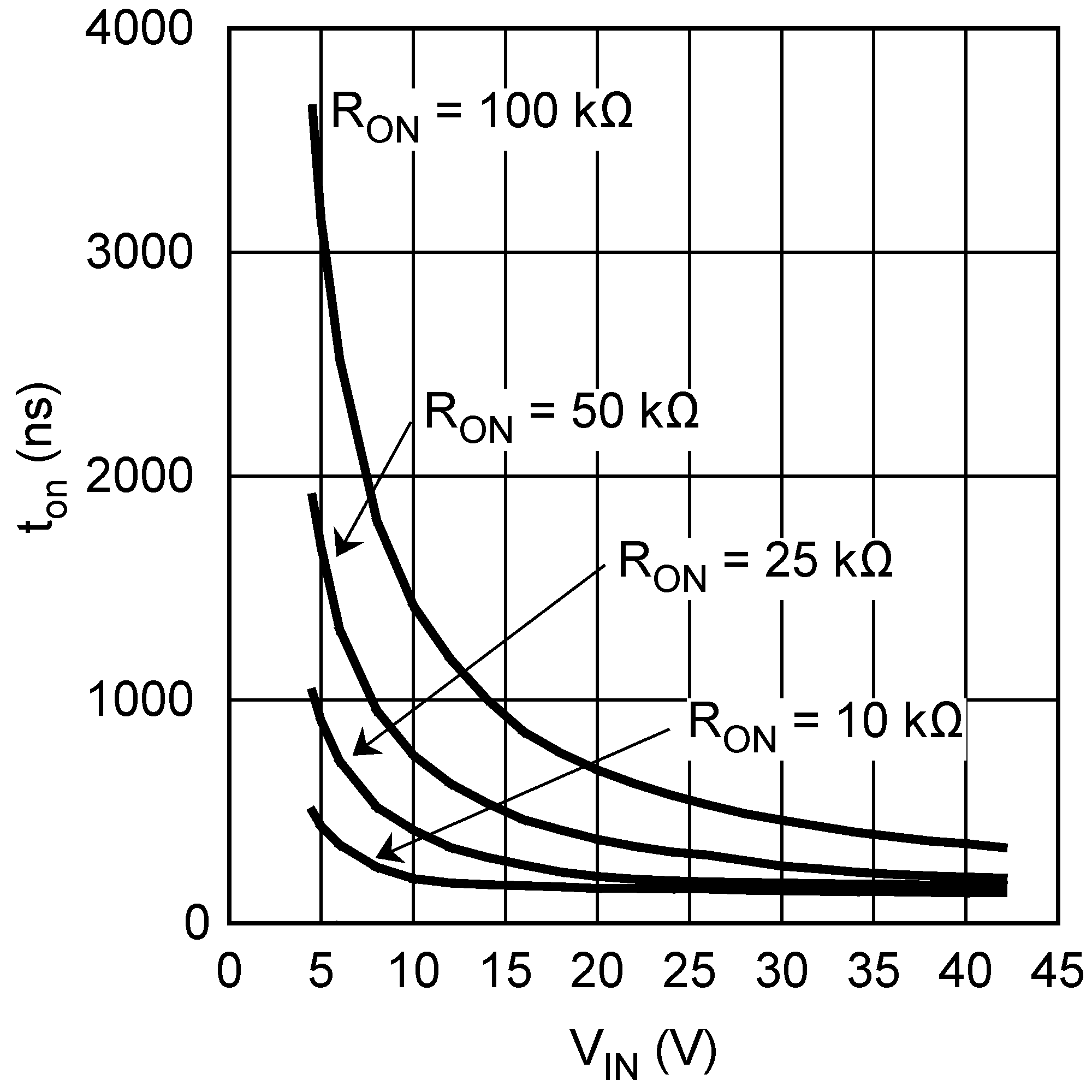
LMR24220 30167606.png
Figure 3. ton vs VIN
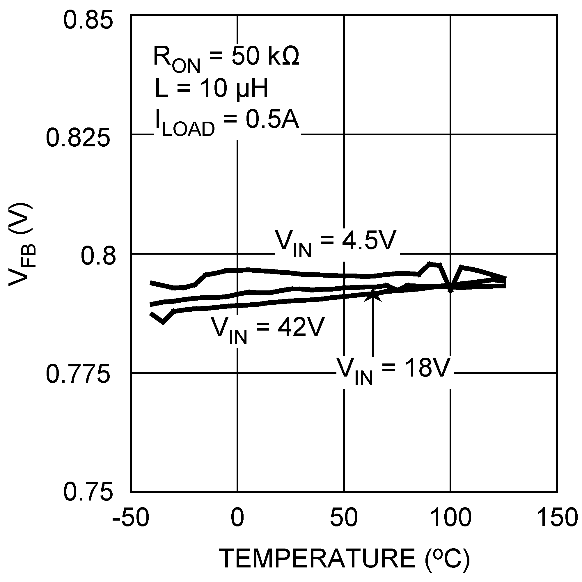
LMR24220 30167608.png
Figure 5. VFB vs Temperature
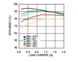
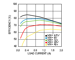
LMR24220 30167670.gif
VOUT = 3.3 V
Figure 7. Efficiency vs Load Current
LMR24220 30167672.gif
VOUT = 0.8 V
Figure 9. Efficiency vs Load Current
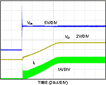
LMR24220 30167676.gif
VOUT = 3.3 V, 2 A Loaded
Figure 11. Power Up
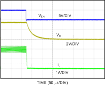
LMR24220 30167615.gif
VOUT = 3.3 V, 2 A Loaded
Figure 13. Shutdown Transient
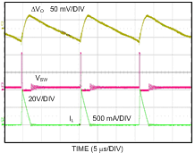
LMR24220 30167617.gif
VOUT = 3.3 V, 0.5 A Loaded
Figure 15. Discontinuous Mode Operation
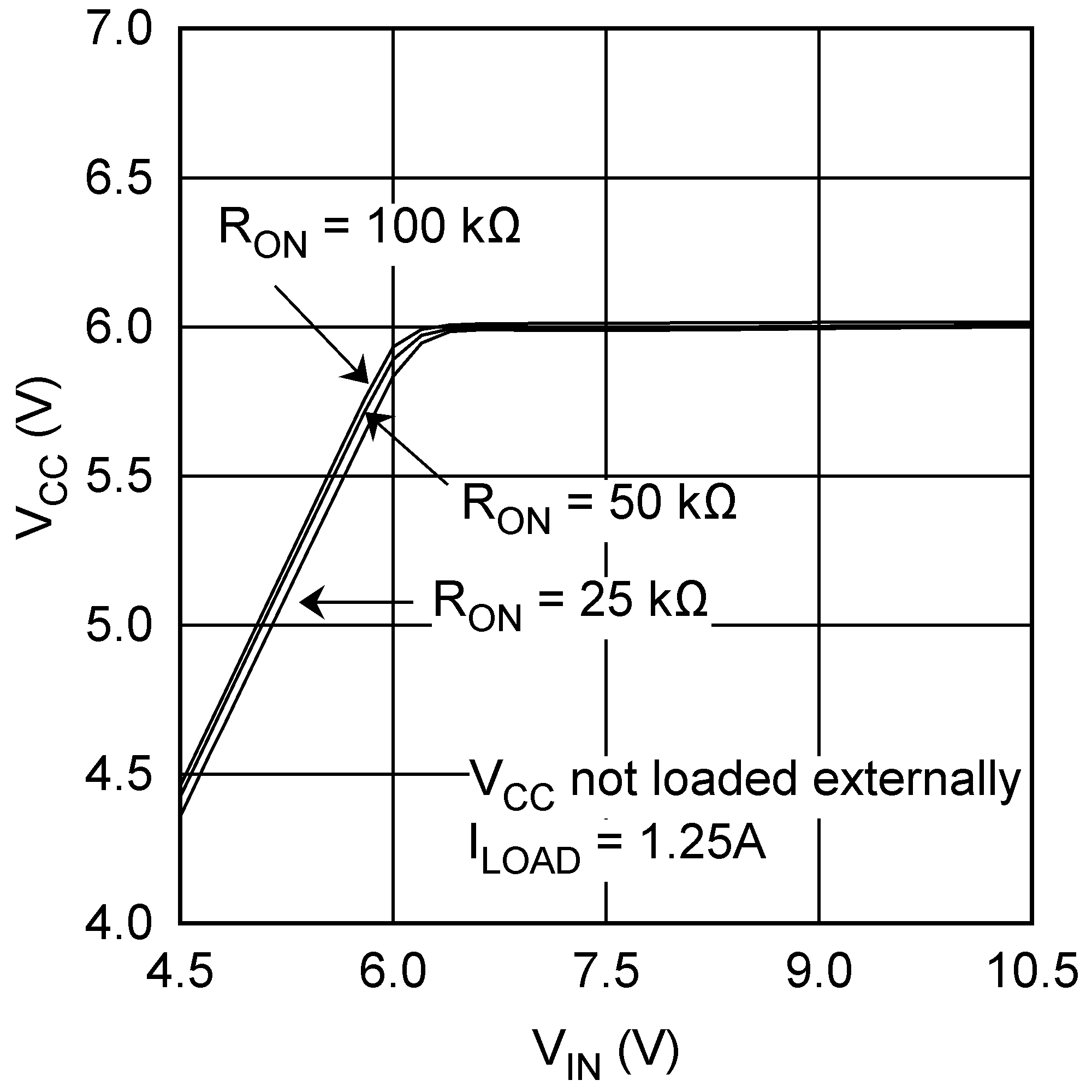
LMR24220 30167605.png
Figure 2. VCC vs VIN
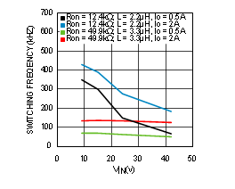
LMR24220 30167675.gif
VOUT = 0.8 V
Figure 4. Switching Frequency, ƒSW vs VIN
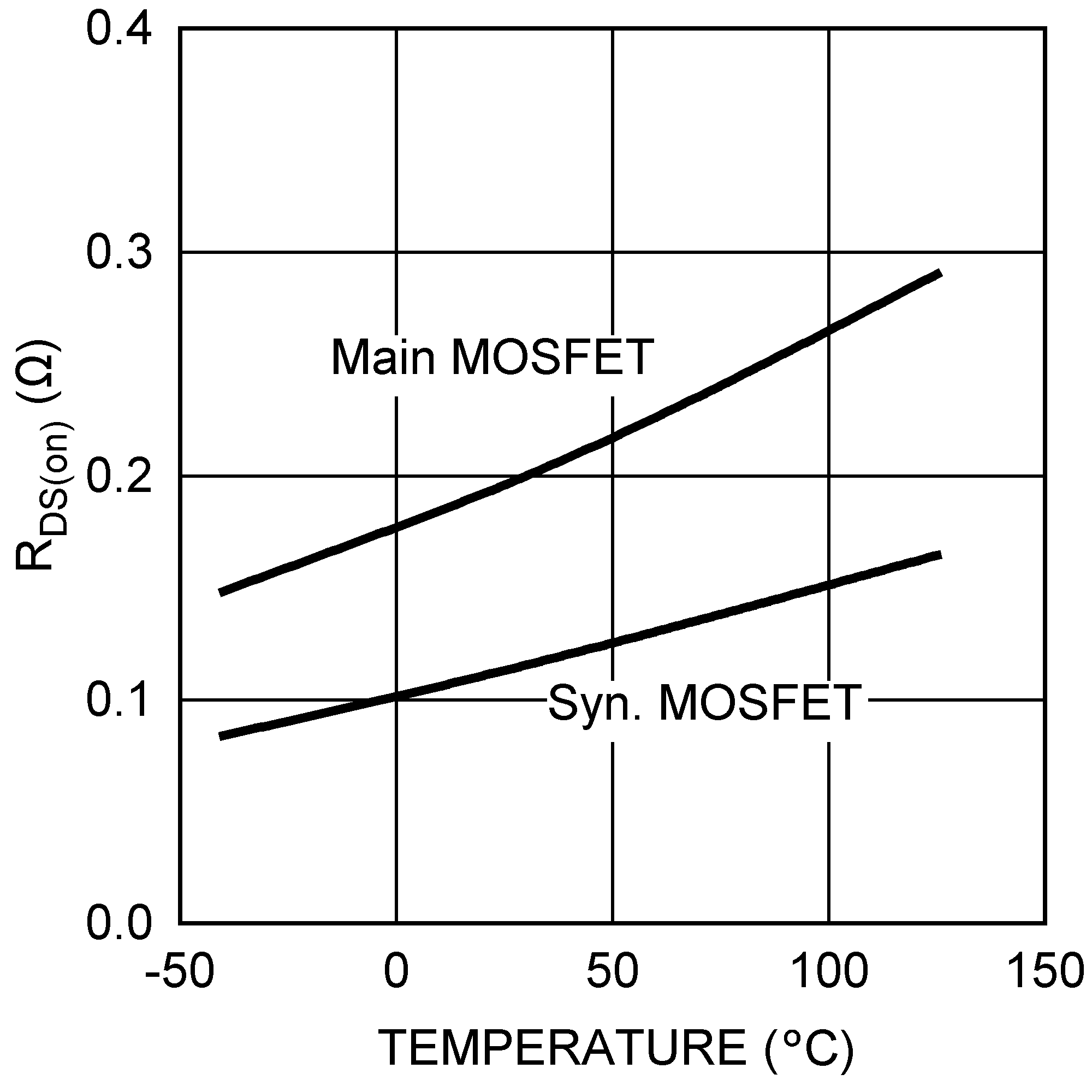
LMR24220 30167609.png
Figure 6. RDS(on) vs Temperature
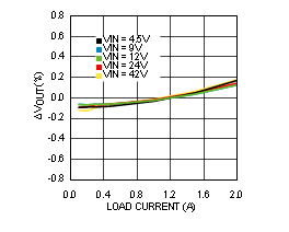
LMR24220 30167671.gif
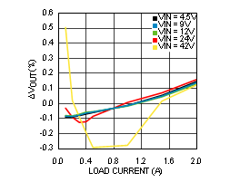
VOUT = 3.3 V
Figure 8. VOUT Regulation vs Load Current
LMR24220 30167673.gif
VOUT = 0.8 V
Figure 10. VOUT Regulation vs Load Current
LMR24220 30167614.gif
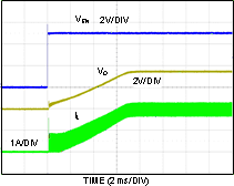
VOUT = 3.3 V, 2 A Loaded
Figure 12. Start-up With Enable
LMR24220 30167616.gif
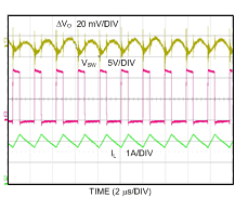
VOUT = 3.3 V, 2 A Loaded
Figure 14. Continuous Mode Operation
LMR24220 30167618.gif
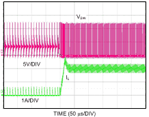
VOUT = 3.3 V, 0.5 A to 2 A Loaded
Figure 16. DCM to CCM Transition