JAJSF76D September   2015  – June 2018 LMZ36002

PRODUCTION DATA.  

  1. 特長
  2. アプリケーション
  3. 概要
    1.     Device Images
      1.      アプリケーション概略図
      2.      効率と出力電流との関係
  4. 改訂履歴
  5. Pin Configuration and Functions
    1.     Pin Functions
  6. Specifications
    1. 6.1  Absolute Maximum Ratings
    2. 6.2  ESD Ratings
    3. 6.3  Recommended Operating Conditions
    4. 6.4  Thermal Information
    5. 6.5  Electrical Characteristics
    6. 6.6  Switching Characteristics
    7. 6.7  Typical Characteristics
    8. 6.8  Typical Characteristics
    9. 6.9  Typical Characteristics
    10. 6.10 Typical Characteristics (Thermal Derating)
  7. Detailed Description
    1. 7.1 Overview
    2. 7.2 Functional Block Diagram
    3. 7.3 Feature Description
      1. 7.3.1  Adjusting the Output Voltage
      2. 7.3.2  Switching Frequency (RT)
      3. 7.3.3  Recommended Operating Range
      4. 7.3.4  Synchronization (CLK)
      5. 7.3.5  Output Capacitor Selection
      6. 7.3.6  VERSA-COMP Pin Configurations
      7. 7.3.7  Input Capacitor Selection
      8. 7.3.8  Output On/Off Inhibit (INH/UVLO)
      9. 7.3.9  Under Voltage Lockout (UVLO)
      10. 7.3.10 Remote Sense
      11. 7.3.11 VBSEL
      12. 7.3.12 Soft-Start (SS/TR)
      13. 7.3.13 Power Good (PWRGD) and Pull-up (PWRGD_PU)
      14. 7.3.14 Overcurrent Protection
      15. 7.3.15 Thermal Shutdown
    4. 7.4 Device Functional Modes
      1. 7.4.1 Active Mode
      2. 7.4.2 Light Load Operation
      3. 7.4.3 Shutdown Mode
  8. Application and Implementation
    1. 8.1 Application Information
      1. 8.1.1 Minimum External Component Application
        1. 8.1.1.1 Design Requirements
        2. 8.1.1.2 Detailed Design Procedure
          1. 8.1.1.2.1 Custom Design With WEBENCH® Tools
          2. 8.1.1.2.2 Output Voltage Set-Point
          3. 8.1.1.2.3 RT and RTSEL
          4. 8.1.1.2.4 VERSA-COMP
          5. 8.1.1.2.5 VBSEL
          6. 8.1.1.2.6 Input Capacitors
          7. 8.1.1.2.7 Output Capacitors
          8. 8.1.1.2.8 Application Curves
      2. 8.1.2 Typical Application
        1. 8.1.2.1 Design Requirements
      3. 8.1.3 Detailed Design Procedure
        1. 8.1.3.1 Switching Frequency
        2. 8.1.3.2 Power Good
        3. 8.1.3.3 Inhibit Control
        4. 8.1.3.4 VERSA-COMP
        5. 8.1.3.5 VBSEL
        6. 8.1.3.6 Soft-Start Capacitors
        7. 8.1.3.7 Input Capacitors
        8. 8.1.3.8 Output Capacitors
  9. Power Supply Recommendations
  10. 10Layout
    1. 10.1 Layout Guidelines
    2. 10.2 Layout Example
    3. 10.3 EMI
  11. 11デバイスおよびドキュメントのサポート
    1. 11.1 デバイス・サポート
      1. 11.1.1 開発サポート
        1. 11.1.1.1 WEBENCH®ツールによるカスタム設計
      2. 11.1.2 デベロッパー・ネットワークの製品に関する免責事項
    2. 11.2 ドキュメントの更新通知を受け取る方法
    3. 11.3 コミュニティ・リソース
    4. 11.4 商標
    5. 11.5 静電気放電に関する注意事項
    6. 11.6 Glossary
  12. 12メカニカル、パッケージ、および注文情報

パッケージ・オプション

メカニカル・データ(パッケージ|ピン)
サーマルパッド・メカニカル・データ
発注情報

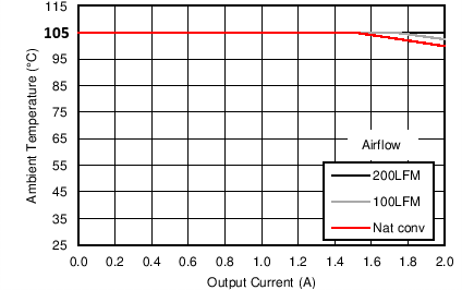
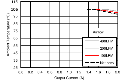
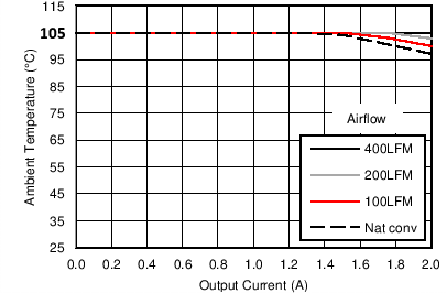
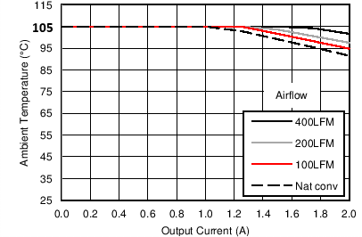
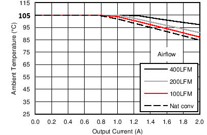
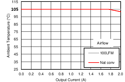
Typical Characteristics (Thermal Derating)

The temperature derating curves represent the conditions at which internal components are at or below the manufacturer's maximum operating temperatures. Derating limits apply to devices soldered directly to a 50 mm × 100 mm, 4-layer PCB with 2 oz. copper.
LMZ36002 24Vin_33Vo_250k_SOA.png
PVIN = 24 V VOUT = 3.3 V
Figure 19. Safe Operating Area
LMZ36002 24Vin_5Vo_250k_SOA.png
PVIN = 24 V VOUT = 5 V
Figure 21. Safe Operating Area
LMZ36002 24Vin_75Vo_400k_SOA.png
PVIN = 24 V VOUT = 7.5 V
Figure 23. Safe Operating Area
LMZ36002 48Vin_33Vo_250k_SOA.png
PVIN = 48 V VOUT = 3.3 V
Figure 20. Safe Operating Area
LMZ36002 48Vin_5Vo_300k_SOA.png
PVIN = 48 V VOUT = 5 V
Figure 22. Safe Operating Area
LMZ36002 48Vin_75Vo_400k_SOA.png
PVIN = 48 V VOUT = 7.5 V
Figure 24. Safe Operating Area