JAJSF76D September 2015 – June 2018 LMZ36002
PRODUCTION DATA.
- 1 特長
- 2 アプリケーション
- 3 概要
- 4 改訂履歴
- 5 Pin Configuration and Functions
- 6 Specifications
-
7 Detailed Description
- 7.1 Overview
- 7.2 Functional Block Diagram
- 7.3
Feature Description
- 7.3.1 Adjusting the Output Voltage
- 7.3.2 Switching Frequency (RT)
- 7.3.3 Recommended Operating Range
- 7.3.4 Synchronization (CLK)
- 7.3.5 Output Capacitor Selection
- 7.3.6 VERSA-COMP Pin Configurations
- 7.3.7 Input Capacitor Selection
- 7.3.8 Output On/Off Inhibit (INH/UVLO)
- 7.3.9 Under Voltage Lockout (UVLO)
- 7.3.10 Remote Sense
- 7.3.11 VBSEL
- 7.3.12 Soft-Start (SS/TR)
- 7.3.13 Power Good (PWRGD) and Pull-up (PWRGD_PU)
- 7.3.14 Overcurrent Protection
- 7.3.15 Thermal Shutdown
- 7.4 Device Functional Modes
- 8 Application and Implementation
- 9 Power Supply Recommendations
- 10Layout
- 11デバイスおよびドキュメントのサポート
- 12メカニカル、パッケージ、および注文情報
7.3.8 Output On/Off Inhibit (INH/UVLO)
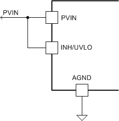
The INH/UVLO pin provides on and off control of the device. The INH input provides a precise 2.1 V as soon as rising threshold to allow direct logic drive or connection to a voltage divider from a higher voltage source such as PVIN. Once the INH/UVLO pin voltage exceeds the threshold voltage, the device starts operation. The INH input also incorporates 300 mV (typ) of hysteresis resulting in a falling threshold of 1.8 V. If the INH/UVLO pin voltage is pulled below the threshold voltage, the regulator stops switching and enters low quiescent current state. The INH/UVLO pin cannot be open circuit or floating. The simplest way to enable the operation of the LMZ36002 is to connect the INH/UVLO pin to PVIN pin directly as shown in Figure 27. This connection allows the LMZ36002 device to restart when PVIN is again within the operation range.
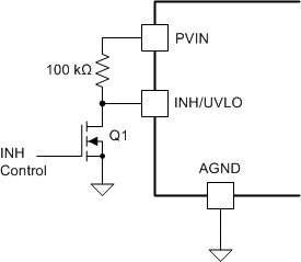
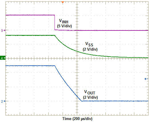
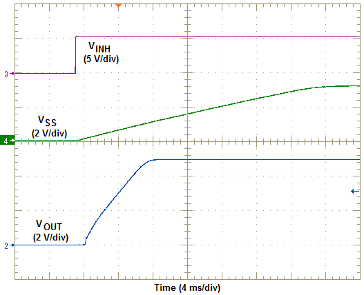
If an application requires controlling the INH/UVLO pin, either drive it directly with a logic input or use an open drain and collector device to interface with the pin and place a 100-kΩ resistor between this pin and PVIN pin as shown in Figure 28. When turning Q1 on applies a low voltage to the inhibit control (INH/UVLO) pin and disables the output of the supply, shown in Figure 29. If Q1 is turned off, the supply executes a soft-start power-up sequence, as shown in Figure 30.
 Figure 27. Enabling the Device
  Figure 28. Typical Inhibit Control
  Figure 29. Inhibit Turn-Off
  Figure 30. Inhibit Turn-On