JAJSF76D September 2015 – June 2018 LMZ36002
PRODUCTION DATA.
- 1 特長
- 2 アプリケーション
- 3 概要
- 4 改訂履歴
- 5 Pin Configuration and Functions
- 6 Specifications
-
7 Detailed Description
- 7.1 Overview
- 7.2 Functional Block Diagram
- 7.3
Feature Description
- 7.3.1 Adjusting the Output Voltage
- 7.3.2 Switching Frequency (RT)
- 7.3.3 Recommended Operating Range
- 7.3.4 Synchronization (CLK)
- 7.3.5 Output Capacitor Selection
- 7.3.6 VERSA-COMP Pin Configurations
- 7.3.7 Input Capacitor Selection
- 7.3.8 Output On/Off Inhibit (INH/UVLO)
- 7.3.9 Under Voltage Lockout (UVLO)
- 7.3.10 Remote Sense
- 7.3.11 VBSEL
- 7.3.12 Soft-Start (SS/TR)
- 7.3.13 Power Good (PWRGD) and Pull-up (PWRGD_PU)
- 7.3.14 Overcurrent Protection
- 7.3.15 Thermal Shutdown
- 7.4 Device Functional Modes
- 8 Application and Implementation
- 9 Power Supply Recommendations
- 10Layout
- 11デバイスおよびドキュメントのサポート
- 12メカニカル、パッケージ、および注文情報
7.3.9 Under Voltage Lockout (UVLO)
The LMZ36002 device has an internal UVLO circuit which prevents the device from operating until the PVIN voltage exceeds the UVLO threshold, (3.2 V (typ)). The device will begin switching and the output voltage will begin to rise once PVIN exceeds the threshold, however PVIN must be greater than (VOUT/0.75) in order to for VOUT to regulate at the set-point voltage.
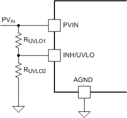
Applications may require a higher UVLO threshold to prevent early turn-on, for sequencing requirements, or to prevent input current draw at lower input voltages. An external resistor divider can be added to the INH/UVLO pin to adjust the UVLO threshold higher. The external resistor divider can be configured as shown in Figure 31. Table 10 lists standard values for RUVLO1 and RUVLO2 to adjust the UVLO voltage higher.
 Figure 31. Adjustable PVIN UVLO
 Table 10. Standard Resistor Values for Adjusting PVIN UVLO
| VIN UVLO (V) | 4.5 | 10 | 15 | 20 | 25 | 30 | 35 | 40 | 45 |
|---|---|---|---|---|---|---|---|---|---|
| RUVLO1 (kΩ) | 100 | 100 | 100 | 100 | 100 | 100 | 100 | 100 | 100 |
| RUVLO2 (kΩ) | 46.4 | 21.0 | 14.0 | 10.5 | 8.45 | 6.98 | 6.04 | 5.23 | 4.64 |