JAJSQD9B january   2015  – june 2023 LV2862

PRODUCTION DATA  

  1.   1
  2. 特長
  3. アプリケーション
  4. 概要
  5. Revision History
  6. Pin Configuration and Functions
  7. Specifications
    1. 6.1 Absolute Maximum Ratings
    2. 6.2 ESD Ratings
    3. 6.3 Recommended Operating Conditions
    4. 6.4 Thermal Information
    5. 6.5 Electrical Characteristics
    6. 6.6 Typical Characteristics
  8. Detailed Description
    1. 7.1 Overview
    2. 7.2 Functional Block Diagram
    3. 7.3 Feature Description
      1. 7.3.1 Continuous Conduction Mode
      2. 7.3.2 Fixed Frequency PWM Control
      3. 7.3.3 Eco-mode
      4. 7.3.4 Bootstrap Voltage (CB)
      5. 7.3.5 Enable (SHDN) and VIN Undervoltage Lockout (UVLO)
      6. 7.3.6 Setting the Output Voltage
      7. 7.3.7 Current Limit
      8. 7.3.8 Thermal Shutdown
    4. 7.4 Device Functional Modes
  9. Application and Implementation
    1. 8.1 Application Information
    2. 8.2 Typical Application
      1. 8.2.1 Design Requirements
        1. 8.2.1.1 Design Guide – Step By Step Design Procedure
      2. 8.2.2 Detailed Design Procedure
        1. 8.2.2.1 Selecting the Switching Frequency
        2. 8.2.2.2 Output Inductor Selection
        3. 8.2.2.3 Output Capacitor Selection
        4. 8.2.2.4 Schottky Diode Selection
        5. 8.2.2.5 Input Capacitor Selection
          1. 8.2.2.5.1 Bootstrap Capacitor Selection
            1. 8.2.2.5.1.1 Typical Application Circuits
      3. 8.2.3 Application Curves
    3. 8.3 Power Supply Recommendations
    4. 8.4 Layout
      1. 8.4.1 Layout Guidelines
      2. 8.4.2 Layout Example
  10. Device and Documentation Support
    1. 9.1 Documentation Support
      1. 9.1.1 Related Documentation
    2. 9.2 ドキュメントの更新通知を受け取る方法
    3. 9.3 サポート・リソース
    4. 9.4 Trademarks
    5. 9.5 静電気放電に関する注意事項
    6. 9.6 用語集
  11. 10Mechanical, Packaging, and Orderable Information

パッケージ・オプション

メカニカル・データ(パッケージ|ピン)
サーマルパッド・メカニカル・データ
発注情報

Input Capacitor Selection

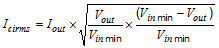
A low ESR ceramic capacitor is needed between the VIN pin and ground pin. This capacitor prevents large voltage transients from appearing at the input. Use a 2.2 µF–10 µF value with X5R or X7R dielectric. Depending on construction, the value of a ceramic capacitor can decrease up to 50% of its nominal value when rated voltage is applied. Consult with the capacitor manufacturer's data sheet for information on capacitor derating over voltage and temperature. The capacitor must also have a ripple current rating greater than the maximum input current ripple of the LV2862. The input ripple current can be calculated using Equation 10 and Equation 11.

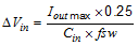
For this example design, one 4.7-µF, 50-V capacitor is selected. The input capacitance value determines the input ripple voltage of the regulator. The input voltage ripple can be calculated using Equation 10. Using the design example values, Ioutmax = 0.6 A, Cin = 2.2 µF, and fsw = 770 kHz yields an input voltage ripple of 97 mV and an RMS input ripple current of 0.3 A.

Equation 10. GUID-B7901C62-9202-425E-8109-DF3314C90921-low.gif
Equation 11. GUID-FC92C0D9-D669-42B8-9A4F-D5B88C6BE66D-low.gif