JAJSQD9B january 2015 – june 2023 LV2862
PRODUCTION DATA
- 1
- 1 特長
- 2 アプリケーション
- 3 概要
- 4 Revision History
- 5 Pin Configuration and Functions
- 6 Specifications
- 7 Detailed Description
- 8 Application and Implementation
- 9 Device and Documentation Support
- 10Mechanical, Packaging, and Orderable Information
8.2.2.3 Output Capacitor Selection
The selection of COUT is mainly driven by three primary considerations. The output capacitor determines the modulator pole, the output voltage ripple, and how the regulator responds to a large change in load current. The output capacitance needs to be selected based on the most stringent of these three criteria.
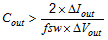
The first criterion is the desired response to a large change in the load current. The regulator usually needs two or more clock cycles for the control loop to see the change in load current and output voltage and adjust the duty cycle to react to the change. The output capacitance must be large enough to supply the difference in current for two clock cycles while only allowing a tolerable amount of droop in the output voltage. Equation 5 shows the minimum output capacitance necessary to accomplish this. The transient load response is specified as a 3% change in VOUT for a load step from 0.03 A to 0.6 A (full load), ΔIOUT = 0.6 - 0.03 = 0.57 A and ΔVOUT = 0.03 × 5 = 0.15 V. Using these numbers gives a minimum capacitance of 10.8 µF. For ceramic capacitors, the ESR is usually small enough to ignore in this calculation. Aluminum electrolytic and tantalum capacitors have higher ESR that must be taken into account.
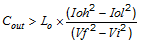
The stored energy in the inductor produces an output voltage overshoot when the load current rapidly decreases. The output capacitor must also be sized to absorb energy stored in the inductor when transitioning from a high load current to a lower load current. Equation 6 is used to calculate the minimum capacitance to keep the output voltage overshoot to a desired value. Where L is the value of the inductor, IOH, is the output current under heavy load, IOL is the output under light load, Vf is the final peak output voltage, and Vi is the initial capacitor voltage. For this example, the worst case load step is from 0.6 A to 0.03 A. The output voltage increases during this load transition and the stated maximum in our specification is 3% of the output voltage. This makes Vo_overshoot = 1.03 × 5 = 5.15 V. Vi is the initial capacitor voltage which is the nominal output voltage of 5 V. Using these numbers in Equation 6 yields a minimum capacitance of 5.2 µF.
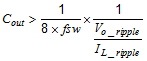
Equation 7 calculates the minimum output capacitance needed to meet the output voltage ripple specification where fSW is the switching frequency, Vo_ripple is the maximum allowable output voltage ripple, and IL_ripple is the inductor ripple current. Equation 7 yields 0.26 µF. Equation 8 calculates the maximum ESR an output capacitor can have to meet the output voltage ripple specification. indicates the ESR must be less than 680 mΩ.
Additional capacitance de-ratings for aging, temperature, and dc bias must be factored in which increases this minimum value. For this example, 10-µF ceramic capacitors are used. Capacitors in the range of 10 µF–100 µF are a good starting point with an ESR of 0.7 Ω or less.