JAJSLI5J January 2011 – March 2021 OPA2835 , OPA835
PRODUCTION DATA
- 1 特長
- 2 アプリケーション
- 3 概要
- 4 Revision History
- 5 Device Comparision Table
- 6 Pin Configuration and Functions
-
7 Specifications
- 7.1 Absolute Maximum Ratings
- 7.2 ESD Ratings
- 7.3 Recommended Operating Conditions
- 7.4 Thermal Information: OPA835
- 7.5 Thermal Information: OPA2835
- 7.6 Electrical Characteristics: VS = 2.7 V
- 7.7 Electrical Characteristics: VS = 5 V
- 7.8 Typical Characteristics: VS = 2.7 V
- 7.9 Typical Characteristics: VS = 5 V
- 8 Detailed Description
-
9 Application and Implementation
- 9.1
Application Information
- 9.1.1 Noninverting Amplifier
- 9.1.2 Inverting Amplifier
- 9.1.3 Instrumentation Amplifier
- 9.1.4 Attenuators
- 9.1.5 Single-Ended to Differential Amplifier
- 9.1.6 Differential to Single-Ended Amplifier
- 9.1.7 Differential-to-Differential Amplifier
- 9.1.8 Gain Setting With OPA835 RUN Integrated Resistors
- 9.1.9 Pulse Application With Single-Supply
- 9.1.10 ADC Driver Performance
- 9.2 Typical Application
- 9.1
Application Information
- 10Power Supply Recommendations
- 11Layout
- 12Device and Documentation Support
- 13Mechanical, Packaging, and Orderable Information
パッケージ・オプション
メカニカル・データ(パッケージ|ピン)
サーマルパッド・メカニカル・データ
発注情報
9.2.2 Active Filters
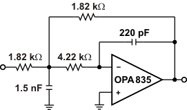
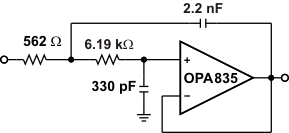
The OPA835 and OPA2835 devices are good choices for active filters. Figure 9-16 and Figure 9-15 show MFB and Sallen-Key circuits designed using the WEBENCH® Filter Designer to implement second-order low-pass Butterworth filter circuits. Figure 9-17 shows the frequency response.
Other MFB and Sallen-Key filter circuits display similar performance. The main difference is the MFB is an inverting amplifier in the pass band and the Sallen-Key is noninverting. The primary advantage for each is the Sallen-Key in unity gain has no resistor gain error term, and thus no sensitivity to gain error, while the MFB has better attenuation properties beyond the bandwidth of the op amp.
 Figure 9-15 MFB 100-kHz Second-Order Low-Pass Butterworth Filter Circuit
 Figure 9-16 Sallen-Key 100-kHz Second-Order Low-Pass Butterworth Filter Circuit