JAJSLI5J January 2011 – March 2021 OPA2835 , OPA835
PRODUCTION DATA
- 1 特長
- 2 アプリケーション
- 3 概要
- 4 Revision History
- 5 Device Comparision Table
- 6 Pin Configuration and Functions
-
7 Specifications
- 7.1 Absolute Maximum Ratings
- 7.2 ESD Ratings
- 7.3 Recommended Operating Conditions
- 7.4 Thermal Information: OPA835
- 7.5 Thermal Information: OPA2835
- 7.6 Electrical Characteristics: VS = 2.7 V
- 7.7 Electrical Characteristics: VS = 5 V
- 7.8 Typical Characteristics: VS = 2.7 V
- 7.9 Typical Characteristics: VS = 5 V
- 8 Detailed Description
-
9 Application and Implementation
- 9.1
Application Information
- 9.1.1 Noninverting Amplifier
- 9.1.2 Inverting Amplifier
- 9.1.3 Instrumentation Amplifier
- 9.1.4 Attenuators
- 9.1.5 Single-Ended to Differential Amplifier
- 9.1.6 Differential to Single-Ended Amplifier
- 9.1.7 Differential-to-Differential Amplifier
- 9.1.8 Gain Setting With OPA835 RUN Integrated Resistors
- 9.1.9 Pulse Application With Single-Supply
- 9.1.10 ADC Driver Performance
- 9.2 Typical Application
- 9.1
Application Information
- 10Power Supply Recommendations
- 11Layout
- 12Device and Documentation Support
- 13Mechanical, Packaging, and Orderable Information
パッケージ・オプション
メカニカル・データ(パッケージ|ピン)
サーマルパッド・メカニカル・データ
発注情報
9.1.9 Pulse Application With Single-Supply
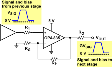
For pulsed applications where the signal is at ground and pulses to a positive or negative voltage, the circuit bias-voltage considerations differ from those in an application with a signal that swings symmetrically about a reference point. Figure 9-7 shows a circuit where the signal is at ground (0 V) and pulses to a positive value.
 Figure 9-7 Noninverting Single Supply With Pulse
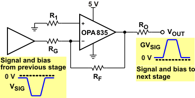
If the input signal pulses negative from ground, an inverting amplifier is more appropriate, as shown in Figure 9-8. A key consideration in noninverting and inverting cases is that the input and output voltages are kept within the limits of the amplifier. Because the VICR of the OPA835 device includes the negative supply rail, the OPA835 op amp is well-suited for this application.
 Figure 9-8 Inverting
Single Supply With Pulse