SBOS688A April 2015 – October 2015 OPA2625 , OPA625
PRODUCTION DATA.
- 1 Features
- 2 Applications
- 3 Description
- 4 Revision History
- 5 Pin Configuration and Functions
-
6 Specifications
- 6.1 Absolute Maximum Ratings
- 6.2 ESD Ratings
- 6.3 Recommended Operating Conditions
- 6.4 Thermal Information
- 6.5 Electrical Characteristics High-Drive Mode
- 6.6 Electrical Characteristics Low-Power Mode
- 6.7 Electrical Characteristics High-Drive Mode
- 6.8 Electrical Characteristics Low-Power Mode
- 6.9 Switching Characteristics
- 6.10 Typical Characteristics
- 7 Parameter Measurement Information
- 8 Detailed Description
- 9 Application and Implementation
- 10Power Supply Recommendations
- 11Layout
- 12Device and Documentation Support
- 13Mechanical, Packaging, and Orderable Information
9 Application and Implementation
NOTE
Information in the following applications sections is not part of the TI component specification, and TI does not warrant its accuracy or completeness. TI’s customers are responsible for determining suitability of components for their purposes. Customers should validate and test their design implementation to confirm system functionality.
9.1 Application Information
The OPAx625 is a precision, high-speed, voltage-feedback operational amplifier. Fast settling to 16-bit levels, low THD, and low noise make the OPAx625 suitable for driving SAR ADC inputs and buffering precision voltage references. With a wide power-supply voltage range from 2.7 V to 5.5 V, and operating from –40°C to +125°C, the OPAx625 is suitable for a variety of high-speed, industrial applications. The following sections show application information for the OPAx625. For simplicity, power-supply decoupling capacitors are not shown in these diagrams.
9.2 Typical Applications
9.2.1 Single-Supply, 16-Bit, 1-MSPS SAR ADC Driver
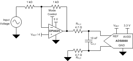 Figure 73. Single-Supply, 16-Bit, 1-MSPS SAR ADC Driver
9.2.1.1 Design Requirements
SAR ADCs, such as the ADS8860, use sampling capacitors on the data converter input. During the signal acquisition phase, these sampling capacitors are connected to the ADC analog input terminals, AINP and AINN, through a set of switches. After the acquisition period has elapsed, the internal sampling capacitors are disconnected from the input terminals and connected to the input of the ADC through a second set of switches, during this period the ADC is performing the analog-to-digital conversion. Figure 74 illustrates this architecture.
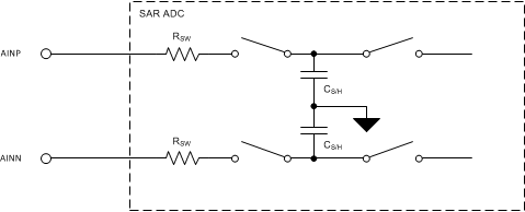 Figure 74. Simplified SAR ADC Input
The SAR ADC inputs and sampling capacitors must be driven by the OPA625 to 16-bit levels within the acquisition time of the ADC. For the example illustrated in Figure 73, the OPA625 is used to drive the ADS8860 at a sample rate of 1 MSPS.
9.2.1.2 Detailed Design Procedure
The circuit illustrated in Figure 73 consists of the SAR ADC driver, a low-pass filter and the SAR ADC. The SAR ADC driver circuit consists of an OPA625 configured in an inverting gain of 1. The filter consists of RFLT and CFLT, connected between the output of the OPA625 and input of the ADS8860. Selecting the proper values for each of these passive components is critical to obtain the best performance from the ADC. Capacitor CFLT serves as a charge reservoir, providing the necessary charge to the ADC sampling capacitors. The dynamic load presented by the ADC creates a glitch on the filter capacitor, CFLT. To minimize the magnitude of this glitch, choose a value for CFLT large enough to maintain a glitch amplitude of less than 100 mV. Maintaining such a low glitch amplitude at the amplifier output makes sure that the amplifier remains in the linear operating region, and results in a minimum settling time. Using Equation 6, a 10-nF capacitor is selected for CFLT.

Connecting a 10-nF capacitor directly to the output of the OPA625 degrades the OPA625 phase margin and results in stability and settling-time problems. To properly drive the 10-nF capacitor, use a series resistor (RFLT) to isolate the capacitor, CFLT, from the OPA625. RFLT must be sized based upon several constraints. To determination a suitable value for RFLT, consider the impact upon the THD due to the voltage divider effect from RFLT reacting with the switch resistance (RSW) of the ADC input circuit, as well as the impact of the output impedance upon amplifier stability. In this example, 4.7-Ω resistors are selected. In this design example, Figure 16 can be used to estimate a suitable value for RISO. RISO represents the total resistance in series with CFLT, and in this example is equivalent to 2 × RFLT.
 |
For step-by-step design procedure, circuit schematics, bill of materials, printed circuit board (PCB) files, simulation results, and test results, refer to TI Precision Design, TIDU014, "Power-optimized 16-bit 1MSPS Data Acquisition Block for Lowest Distortion and Noise Reference Design". |
9.2.2 Single-Supply, 16-Bit, 1-MSPS, Multiplexed, SAR ADC Driver
In order to operate a high-resolution, 16-bit ADC at its maximum throughput, the full-scale voltage step must settle to better than 16-bit accuracy at the ADC inputs within the minimum specified acquisition time (tACQ). This settling imposes very stringent requirements on the driver amplifier in terms of large-signal bandwidth, slew rate, and settling time. Figure 76 illustrates a typical multiplexed ADC driver application using the OPA625.
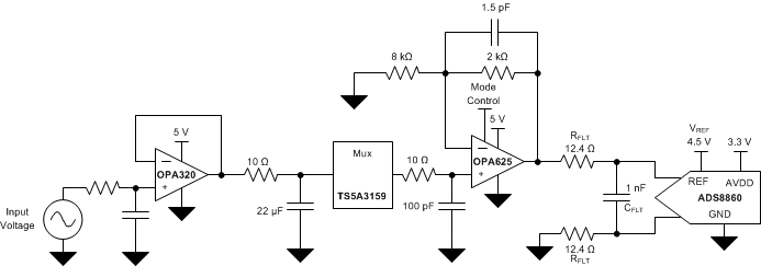 Figure 76. Single-Supply, 16-Bit, 1-MSPS, Multiplexed, SAR ADC Driver
9.2.2.1 Design Requirements
To optimize this circuit for performance, this design does not allow any large signal input transients at the inputs of the driver circuit for a small quiet-time period (tQT) towards the end of the previous conversion. The input step voltage can appear anytime from the beginning of conversion (CONVST rising edge) until the elapse of a half cycle time (0.5 × tCYC). This timing constraint on the input step allows a minimum settling time of (tQT + tACQ) for the ADC input to settle within the required accuracy, in the worst-case scenario. This provides more time for the amplifier's output to slew and settle within the required accuracy before the next conversion starts. Figure 77 illustrates this timing sequence.
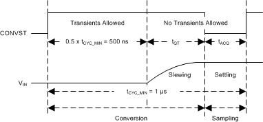 Figure 77. Timing Diagram for Input Signals
9.2.2.2 Detailed Design Procedure
An ADC input driver circuit mainly consists of two parts: a driving amplifier and a fly-wheel RC filter. The amplifier is used for signal conditioning of the input voltage and its low output impedance provides a buffer between the signal source and the ADC input. The RC filter helps attenuate the sampling charge-injection from the switched-capacitor input stage of the ADC as well as acts as an anti-aliasing filter to band-limit the wideband noise contributed by the front-end circuit. The design of the ADC input driver involves optimizing the bandwidth of the circuit, driven primarily by the following requirements:
- The RFLTCFLT filter bandwidth should be low to band-limit the noise fed into the input of the ADC thereby increasing the signal-to-noise ratio (SNR) of the system.
- The overall system bandwidth should be large enough to accommodate optimal settling of the input signal at the ADC input before the start of conversion.
CFLT is chosen based upon Equation 7 . CFLT is chosen to be 1 nF.

Connecting a 1-nF capacitor directly to the output of the OPA625 would degrade the OPA625 phase margin and result in stability and settling time problems. To properly drive the 1-nF capacitor, a series resistor, RFLT, is used to isolate the capacitor, CFLT, from the OPA625. RFLT must be sized based upon several constraints. To determination a suitable value for RFLT, the system designer must consider the impact upon the THD due to the voltage divider effect from RFLT reacting with the switch resistance, RSW, of the ADC input circuit as well as the impact of the output impedance upon amplifier stability. In this example 12.4-Ω resistors are selected. In this design example, Figure 15 can be used to estimate a suitable value for RISO. RISO represents the total resistance in series with CFLT, which in this example is equivalent to 2 × RFLT.
 |
For step-by-step design procedure, circuit schematics, bill of materials, printed circuit board (PCB) files, simulation results, and test results, refer to TI Precision Design, TIDU012, "Power-optimized 16-bit 1MSPS Data Acquisition Block for Lowest Distortion and Noise Reference Design". |
