JAJSP09B August 2022 – January 2023 SN74LV273A-Q1
PRODUCTION DATA
- 1 特長
- 2 アプリケーション
- 3 概要
- 4 Revision History
- 5 Pin Configuration and Functions
-
6 Specifications
- 6.1 Absolute Maximum Ratings
- 6.2 ESD Ratings
- 6.3 Recommended Operating Conditions
- 6.4 Thermal Information
- 6.5 Electrical Characteristics
- 6.6 Timing Requirements, VCC = 2.5 V ± 0.2 V
- 6.7 Timing Requirements, VCC = 3.3 V ± 0.3 V
- 6.8 Timing Requirements, VCC = 5 V ± 0.5 V
- 6.9 Switching Characteristics, VCC = 2.5 V ± 0.2 V
- 6.10 Switching Characteristics, VCC = 3.3 V ± 0.3 V
- 6.11 Switching Characteristics, VCC = 5 V ± 0.5 V
- 6.12 Operating Characteristics
- 6.13 Noise Characteristics
- 6.14 Typical Characteristics
- 7 Parameter Measurement Information
- 8 Detailed Description
- 9 Application and Implementation
- 10Device and Documentation Support
- 11Mechanical, Packaging, and Orderable Information
パッケージ・オプション
メカニカル・データ(パッケージ|ピン)
サーマルパッド・メカニカル・データ
- RKS|20
発注情報
5 Pin Configuration and Functions
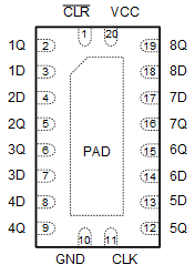
 Figure 5-1 SN74LV273A-Q1 WRKS Package,20-Pin WQFN(Top View)
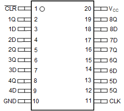
 Figure 5-2 SN74LV273A-Q1 DGS
Package,20-Pin VSSOP(Top View)
Figure 5-2 SN74LV273A-Q1 DGS
Package,20-Pin VSSOP(Top View)Table 5-1 Pin Functions
| PIN | TYPE(1) | DESCRIPTION | |
|---|---|---|---|
| NAME | NO. | ||
| CLR | 1 | I | Clear for all channels, active low |
| 1Q | 2 | O | Output for channel 1 |
| 1D | 3 | I | Input for channel 1 |
| 2D | 4 | I | Input for channel 2 |
| 2Q | 5 | O | Output for channel 2 |
| 3Q | 6 | O | Output for channel 3 |
| 3D | 7 | I | Input for channel 3 |
| 4D | 8 | I | Input for channel 4 |
| 4Q | 9 | O | Output for channel 4 |
| GND | 10 | G | Ground |
| CLK | 11 | I | Clock for all channels, rising edge triggered |
| 5Q | 12 | O | Output for channel 5 |
| 5D | 13 | I | Input for channel 5 |
| 6D | 14 | I | Input for channel 6 |
| 6Q | 15 | O | Output for channel 6 |
| 7Q | 16 | O | Output for channel 7 |
| 7D | 17 | I | Input for channel 7 |
| 8D | 18 | I | Input for channel 8 |
| 8Q | 19 | O | Output for channel 8 |
| VCC | 20 | P | Positive supply |
| Thermal pad | — | Thermal Pad(2) | |
(1) I = Input, O = Output, I/O = Input or Output, G = Ground, P = Power.
(2) WRKS Package Only