JAJSQG7 june 2023 SN75LVPE3410
PRODUCTION DATA
- 1
- 1特長
- 2アプリケーション
- 3概要
- 4Revision History
- 5Pin Configuration and Functions
- 6Specifications
- 7Detailed Description
- 8Application and Implementation
- 9Device and Documentation Support
- Mechanical, Packaging, and Orderable Information
8.2.1.3 Application Curves
The SN75LVPE3410 is a linear redriver that can be used to extend channel reach of a PCIe link. Normally, PCIe-compliant TX and RX are equipped with signal-conditioning functions and can handle channel losses of up to 22 dB at 4 GHz. With the SN75LVPE3410, the total channel loss between a PCIe root complex and an end point can be up to 32 dB at 4 GHz.
 Figure 8-4 Test Setup to Demonstrate
PCIe 3.0 Link Reach Extension Using SN75LVPE3410 - (a) Baseline Setup, (b)
With Redriver
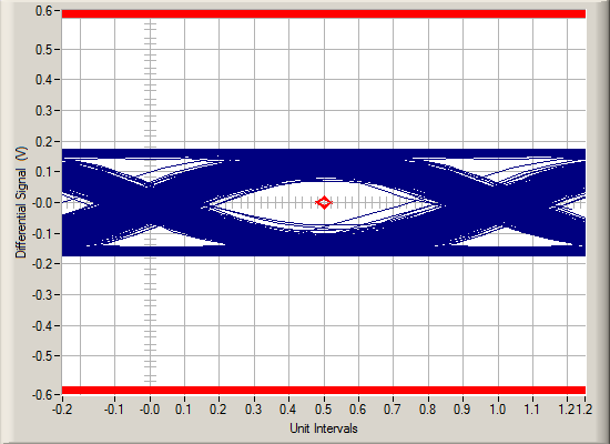
 Figure 8-4 shows a test setup to demonstrate reach extension capability of SN75LVPE3410 as PCIe 3.0 redriver. Table 8-1 provides the test results. As can be seen SN75LVPE3410 provide reach extension such a way that a PCIe 3.0 link with 34 dB total loss passes sigtest compliance requirements. Figure 8-5 shows eye diagram from PCIe 3.0 sigtest tool.
| Setup | Total Link Loss | Minimum Eye Width | Composite Eye Height | PCIe 3.0 Sigtest Result |
|---|---|---|---|---|
| Baseline setup - no redriver | 22 dB | 62 ps | 88 mV | Pass |
| Link with redriver | 34 dB | 37 ps | 141 mV | Pass |
 Figure 8-5 PCIe 3.0 Sigtest Eye
Diagram with 34 dB Total Loss Using SN75LVPE3410