JAJSKD3 november   2020 TAS6424MS-Q1

PRODUCTION DATA  

  1.   1
  2. 特長
  3. アプリケーション
  4. 概要
  5. Revision History
  6. Device Options
  7. Pin Configuration and Functions
  8. Specifications
    1. 7.1 Absolute Maximum Ratings
    2. 7.2 ESD 定格
    3. 7.3 Recommended Operating Conditions
    4. 7.4 Thermal Information
    5. 7.5 Electrical Characteristics
    6. 7.6 Typical Characteristics
  9. Parameter Measurement Information
  10. Detailed Description
    1. 9.1 Overview
    2. 9.2 Functional Block Diagram
    3. 9.3 Feature Description
      1. 9.3.1  Serial Audio Port
        1. 9.3.1.1 I2S Mode
        2. 9.3.1.2 Left-Justified Timing
        3. 9.3.1.3 Right-Justified Timing
        4. 9.3.1.4 TDM Mode
        5. 9.3.1.5 Supported Clock Rates
        6. 9.3.1.6 Audio-Clock Error Handling
      2. 9.3.2  High-Pass Filter
      3. 9.3.3  Volume Control and Gain
      4. 9.3.4  High-Frequency Pulse-Width Modulator (PWM)
      5. 9.3.5  Channel-to-Channel Phase Control
      6. 9.3.6  Gate Drive
      7. 9.3.7  Power FETs
      8. 9.3.8  Load Diagnostics
        1. 9.3.8.1 DC Load Diagnostics
        2. 9.3.8.2 Line Output Diagnostics
        3. 9.3.8.3 AC Load Diagnostics
          1. 9.3.8.3.1 Impedance Magnitude Measurement
          2. 9.3.8.3.2 Impedance Phase Reference Measurement
          3. 9.3.8.3.3 Impedance Phase Measurement
      9. 9.3.9  Protection and Monitoring
        1. 9.3.9.1 Overcurrent Limit (ILIMIT)
        2. 9.3.9.2 Overcurrent Shutdown (ISD)
        3. 9.3.9.3 DC Detect
        4. 9.3.9.4 Clip Detect
        5. 9.3.9.5 Global Overtemperature Warning (OTW), Overtemperature Shutdown (OTSD)
        6. 9.3.9.6 Channel Overtemperature Warning [OTW(i)] and Shutdown [OTSD(i)]
        7. 9.3.9.7 Undervoltage (UV) and Power-On-Reset (POR)
        8. 9.3.9.8 Overvoltage (OV) and Load Dump
      10. 9.3.10 Power Supply
        1. 9.3.10.1 Vehicle-Battery Power-Supply Sequence
        2. 9.3.10.2 Power-Down Sequence
        3. 9.3.10.3 Boosted Power-Supply Sequence
      11. 9.3.11 Hardware Control Pins
        1. 9.3.11.1 FAULT
        2. 9.3.11.2 WARN
        3. 9.3.11.3 MUTE
        4. 9.3.11.4 STANDBY
    4. 9.4 Device Functional Modes
      1. 9.4.1 Operating Modes and Faults
    5. 9.5 Programming
      1. 9.5.1 I2C Serial Communication Bus
      2. 9.5.2 I2C Bus Protocol
      3. 9.5.3 Random Write
      4. 9.5.4 Sequential Write
      5. 9.5.5 Random Read
      6. 9.5.6 Sequential Read
    6. 9.6 Register Maps
      1. 9.6.1  Mode Control Register (address = 0x00) [default = 0x00]
      2. 9.6.2  Miscellaneous Control 1 Register (address = 0x01) [default = 0x32]
      3. 9.6.3  Miscellaneous Control 2 Register (address = 0x02) [default = 0x62]
      4. 9.6.4  SAP Control (Serial Audio-Port Control) Register (address = 0x03) [default = 0x04]
      5. 9.6.5  Channel State Control Register (address = 0x04) [default = 0x55]
      6. 9.6.6  Channel 1 Through 4 Volume Control Registers (address = 0x05–0x08) [default = 0xCF]
      7. 9.6.7  DC Load Diagnostic Control 1 Register (address = 0x09) [default = 0x00]
      8. 9.6.8  DC Load Diagnostic Control 2 Register (address = 0x0A) [default = 0x11]
      9. 9.6.9  DC Load Diagnostic Control 3 Register (address = 0x0B) [default = 0x11]
      10. 9.6.10 DC Load Diagnostic Report 1 Register (address = 0x0C) [default = 0x00]
      11. 9.6.11 DC Load Diagnostic Report 2 Register (address = 0x0D) [default = 0x00]
      12. 9.6.12 DC Load Diagnostics Report 3 Line Output Register (address = 0x0E) [default = 0x00]
      13. 9.6.13 Channel State Reporting Register (address = 0x0F) [default = 0x55]
      14. 9.6.14 Channel Faults (Overcurrent, DC Detection) Register (address = 0x10) [default = 0x00]
      15. 9.6.15 Global Faults 1 Register (address = 0x11) [default = 0x00]
      16. 9.6.16 Global Faults 2 Register (address = 0x12) [default = 0x00]
      17. 9.6.17 Warnings Register (address = 0x13) [default = 0x20]
      18. 9.6.18 Pin Control Register (address = 0x14) [default = 0x00]
      19. 9.6.19 AC Load Diagnostic Control 1 Register (address = 0x15) [default = 0x00]
      20. 9.6.20 AC Load Diagnostic Control 2 Register (address = 0x16) [default = 0x00]
      21. 9.6.21 AC Load Diagnostic Impedance Report Ch1 through Ch4 Registers (address = 0x17–0x1A) [default = 0x00]
      22. 9.6.22 AC Load Diagnostic Phase Report High Register (address = 0x1B) [default = 0x00]
      23. 9.6.23 AC Load Diagnostic Phase Report Low Register (address = 0x1C) [default = 0x00]
      24. 9.6.24 AC Load Diagnostic STI Report High Register (address = 0x1D) [default = 0x00]
      25. 9.6.25 AC Load Diagnostic STI Report Low Register (address = 0x1E) [default = 0x00]
      26. 9.6.26 Miscellaneous Control 3 Register (address = 0x21) [default = 0x00]
      27. 9.6.27 Clip Control Register (address = 0x22) [default = 0x01]
      28. 9.6.28 Clip Window Register (address = 0x23) [default = 0x14]
      29. 9.6.29 Clip Warning Register (address = 0x24) [default = 0x00]
      30. 9.6.30 ILIMIT Status Register (address = 0x25) [default = 0x00]
      31. 9.6.31 Miscellaneous Control 4 Register (address = 0x26) [default = 0x40]
  11. 10Application Information Disclaimer
    1. 10.1 Application Information
      1. 10.1.1 AM-Radio Band Avoidance
      2. 10.1.2 Parallel BTL Operation (PBTL)
      3. 10.1.3 Demodulation Filter Design
      4. 10.1.4 Line Driver Applications
    2. 10.2 Typical Applications
      1. 10.2.1 BTL Application
        1. 10.2.1.1 Design Requirements
          1. 10.2.1.1.1 Communication
        2. 10.2.1.2 Detailed Design Procedure
          1. 10.2.1.2.1 Hardware Design
          2. 10.2.1.2.2 Digital Input and the Serial Audio Port
          3. 10.2.1.2.3 Bootstrap Capacitors
          4. 10.2.1.2.4 Output Reconstruction Filter
      2. 10.2.2 PBTL Application
        1. 10.2.2.1 Design Requirements
          1. 10.2.2.1.1 Detailed Design Procedure
  12. 11Power Supply Recommendations
  13. 12Layout
    1. 12.1 Layout Guidelines
    2. 12.2 Layout Example
    3. 12.3 Thermal Considerations
  14. 13Device and Documentation Support
    1. 13.1 Documentation Support
    2. 13.2 Related Documentation
    3. 13.3 Receiving Notification of Documentation Updates
    4. 13.4 サポート・リソース
    5. 13.5 商標
    6. 13.6 静電気放電に関する注意事項
    7. 13.7 用語集
  15. 14Mechanical, Packaging, and Orderable Information

パッケージ・オプション

メカニカル・データ(パッケージ|ピン)
サーマルパッド・メカニカル・データ
発注情報

Serial Audio Port

The serial audio port (SAP) receives audio in either I2S, left justified, right justified, or TDM formats.

Settings for the serial audio port are programmed in the SAP control register (address 0x03), see the TAS6424MS-Q1 45-W,​​​ 2-MHz Digital Input 4-Channel Automotive Class-D Audio Amplifier with Load Dump Protection and I2C Diagnostics TAS6424MS-Q1 45W、2MHz デジタル入力、4 チャネル車載用 Class-D オーディオ・アンプ、負荷ダンプ保護および I2C 診断機能搭載 TAS6424MS-Q1 45W、2MHz デジタル入力、4 チャネル車載用 Class-D オーディオ・アンプ、負荷ダンプ保護および I2C 診断機能搭載 特長 特長 アプリケーション アプリケーション 概要 概要 Table of Contents Table of Contents Revision History Revision History Device Options Device Options Pin Configuration and Functions Pin Configuration and Functions Specifications Specifications Absolute Maximum Ratings Absolute Maximum Ratings ESD 定格 ESD 定格 Recommended Operating Conditions Recommended Operating Conditions Thermal Information Thermal Information Electrical Characteristics Electrical Characteristics Typical Characteristics Typical Characteristics Parameter Measurement Information Parameter Measurement Information Detailed Description Detailed Description Overview Overview Functional Block Diagram Functional Block Diagram Feature Description Feature Description Serial Audio Port Serial Audio Port I2S Mode I2S Mode Left-Justified Timing Left-Justified Timing Right-Justified Timing Right-Justified Timing TDM Mode TDM Mode Supported Clock Rates Supported Clock Rates Audio-Clock Error Handling Audio-Clock Error Handling High-Pass Filter High-Pass Filter Volume Control and Gain Volume Control and Gain High-Frequency Pulse-Width Modulator (PWM) High-Frequency Pulse-Width Modulator (PWM) Channel-to-Channel Phase Control Channel-to-Channel Phase Control Gate Drive Gate Drive Power FETs Power FETs Load Diagnostics Load Diagnostics DC Load Diagnostics DC Load Diagnostics Line Output Diagnostics Line Output Diagnostics AC Load Diagnostics AC Load Diagnostics Impedance Magnitude Measurement Impedance Magnitude Measurement Impedance Phase Reference Measurement Impedance Phase Reference Measurement Impedance Phase Measurement Impedance Phase Measurement Protection and Monitoring Protection and Monitoring Overcurrent Limit (ILIMIT) Overcurrent Limit (ILIMIT) Overcurrent Shutdown (ISD) Overcurrent Shutdown (ISD) DC Detect DC Detect Clip Detect Clip Detect Global Overtemperature Warning (OTW), Overtemperature Shutdown (OTSD) Global Overtemperature Warning (OTW), Overtemperature Shutdown (OTSD) Channel Overtemperature Warning [OTW(i)] and Shutdown [OTSD(i)] Channel Overtemperature Warning [OTW(i)] and Shutdown [OTSD(i)] Undervoltage (UV) and Power-On-Reset (POR) Undervoltage (UV) and Power-On-Reset (POR) Overvoltage (OV) and Load Dump Overvoltage (OV) and Load Dump Power Supply Power Supply Vehicle-Battery Power-Supply Sequence Vehicle-Battery Power-Supply Sequence Power-Down Sequence Power-Down Sequence Boosted Power-Supply Sequence Boosted Power-Supply Sequence Hardware Control Pins Hardware Control Pins FAULT FAULT WARN WARN MUTE MUTE STANDBY STANDBY Device Functional Modes Device Functional Modes Operating Modes and Faults Operating Modes and Faults Programming Programming I2C Serial Communication Bus I2C Serial Communication Bus I2C Bus Protocol I2C Bus Protocol Random Write Random Write Sequential Write Sequential Write Random Read Random Read Sequential Read Sequential Read Register Maps Register Maps Mode Control Register (address = 0x00) [default = 0x00] Mode Control Register (address = 0x00) [default = 0x00] Miscellaneous Control 1 Register (address = 0x01) [default = 0x32] Miscellaneous Control 1 Register (address = 0x01) [default = 0x32] Miscellaneous Control 2 Register (address = 0x02) [default = 0x62] Miscellaneous Control 2 Register (address = 0x02) [default = 0x62] SAP Control (Serial Audio-Port Control) Register (address = 0x03) [default = 0x04] SAP Control (Serial Audio-Port Control) Register (address = 0x03) [default = 0x04] Channel State Control Register (address = 0x04) [default = 0x55] Channel State Control Register (address = 0x04) [default = 0x55] Channel 1 Through 4 Volume Control Registers (address = 0x05–0x08) [default = 0xCF] Channel 1 Through 4 Volume Control Registers (address = 0x05–0x08) [default = 0xCF] DC Load Diagnostic Control 1 Register (address = 0x09) [default = 0x00] DC Load Diagnostic Control 1 Register (address = 0x09) [default = 0x00] DC Load Diagnostic Control 2 Register (address = 0x0A) [default = 0x11] DC Load Diagnostic Control 2 Register (address = 0x0A) [default = 0x11] DC Load Diagnostic Control 3 Register (address = 0x0B) [default = 0x11] DC Load Diagnostic Control 3 Register (address = 0x0B) [default = 0x11] DC Load Diagnostic Report 1 Register (address = 0x0C) [default = 0x00] DC Load Diagnostic Report 1 Register (address = 0x0C) [default = 0x00] DC Load Diagnostic Report 2 Register (address = 0x0D) [default = 0x00] DC Load Diagnostic Report 2 Register (address = 0x0D) [default = 0x00] DC Load Diagnostics Report 3 Line Output Register (address = 0x0E) [default = 0x00] DC Load Diagnostics Report 3 Line Output Register (address = 0x0E) [default = 0x00] Channel State Reporting Register (address = 0x0F) [default = 0x55] Channel State Reporting Register (address = 0x0F) [default = 0x55] Channel Faults (Overcurrent, DC Detection) Register (address = 0x10) [default = 0x00] Channel Faults (Overcurrent, DC Detection) Register (address = 0x10) [default = 0x00] Global Faults 1 Register (address = 0x11) [default = 0x00] Global Faults 1 Register (address = 0x11) [default = 0x00] Global Faults 2 Register (address = 0x12) [default = 0x00] Global Faults 2 Register (address = 0x12) [default = 0x00] Warnings Register (address = 0x13) [default = 0x20] Warnings Register (address = 0x13) [default = 0x20] Pin Control Register (address = 0x14) [default = 0x00] Pin Control Register (address = 0x14) [default = 0x00] AC Load Diagnostic Control 1 Register (address = 0x15) [default = 0x00] AC Load Diagnostic Control 1 Register (address = 0x15) [default = 0x00] AC Load Diagnostic Control 2 Register (address = 0x16) [default = 0x00] AC Load Diagnostic Control 2 Register (address = 0x16) [default = 0x00] AC Load Diagnostic Impedance Report Ch1 through Ch4 Registers (address = 0x17–0x1A) [default = 0x00] AC Load Diagnostic Impedance Report Ch1 through Ch4 Registers (address = 0x17–0x1A) [default = 0x00] AC Load Diagnostic Phase Report High Register (address = 0x1B) [default = 0x00] AC Load Diagnostic Phase Report High Register (address = 0x1B) [default = 0x00] AC Load Diagnostic Phase Report Low Register (address = 0x1C) [default = 0x00] AC Load Diagnostic Phase Report Low Register (address = 0x1C) [default = 0x00] AC Load Diagnostic STI Report High Register (address = 0x1D) [default = 0x00] AC Load Diagnostic STI Report High Register (address = 0x1D) [default = 0x00] AC Load Diagnostic STI Report Low Register (address = 0x1E) [default = 0x00] AC Load Diagnostic STI Report Low Register (address = 0x1E) [default = 0x00] Miscellaneous Control 3 Register (address = 0x21) [default = 0x00] Miscellaneous Control 3 Register (address = 0x21) [default = 0x00] Clip Control Register (address = 0x22) [default = 0x01] Clip Control Register (address = 0x22) [default = 0x01] Clip Window Register (address = 0x23) [default = 0x14] Clip Window Register (address = 0x23) [default = 0x14] Clip Warning Register (address = 0x24) [default = 0x00] Clip Warning Register (address = 0x24) [default = 0x00] ILIMIT Status Register (address = 0x25) [default = 0x00] ILIMIT Status Register (address = 0x25) [default = 0x00] Miscellaneous Control 4 Register (address = 0x26) [default = 0x40] Miscellaneous Control 4 Register (address = 0x26) [default = 0x40] Application Information Disclaimer Application Information Disclaimer Application Information Application Information AM-Radio Band Avoidance AM-Radio Band Avoidance Parallel BTL Operation (PBTL) Parallel BTL Operation (PBTL) Demodulation Filter Design Demodulation Filter Design Line Driver Applications Line Driver Applications Typical Applications Typical Applications BTL Application BTL Application Design Requirements Design Requirements Communication Communication Detailed Design Procedure Detailed Design Procedure Hardware Design Hardware Design Digital Input and the Serial Audio Port Digital Input and the Serial Audio Port Bootstrap Capacitors Bootstrap Capacitors Output Reconstruction Filter Output Reconstruction Filter PBTL Application PBTL Application Design Requirements Design Requirements Detailed Design Procedure Detailed Design Procedure Power Supply Recommendations Power Supply Recommendations Layout Layout Layout Guidelines Layout Guidelines Layout Example Layout Example Thermal Considerations Thermal Considerations Device and Documentation Support Device and Documentation Support Documentation Support Documentation Support Related Documentation Related Documentation Receiving Notification of Documentation Updates Receiving Notification of Documentation Updates サポート・リソース サポート・リソース 商標 商標 静電気放電に関する注意事項 静電気放電に関する注意事項 用語集 用語集 Mechanical, Packaging, and Orderable Information Mechanical, Packaging, and Orderable Information 重要なお知らせと免責事項 重要なお知らせと免責事項 TAS6424MS-Q1 45W、2MHz デジタル入力、4 チャネル車載用 Class-D オーディオ・アンプ、負荷ダンプ保護および I2C 診断機能搭載 TAS6424MS-Q1 45W、2MHz デジタル入力、4 チャネル車載用 Class-D オーディオ・アンプ、負荷ダンプ保護および I2C 診断機能搭載TAS6424MS-Q12 特長 車載アプリケーション向けに AEC-Q100 認証済み 温度グレード 1:–40℃~125℃、TA 高度な負荷診断機能 DC 診断を入力クロックなしで実行 インピーダンスおよび位相応答を使った AC 診断によるツイータ検出 CISPR25-L5 EMC 仕様に容易に適合 オーディオ入力 4 チャネルの I2S または 4/8 チャネルの TDM 入力 入力サンプル・レート:44.1kHz、48kHz、96kHz 入力フォーマット:16 ビットから 32 ビットの I2S および TDM オーディオ出力 4 チャネルのブリッジ結合負荷 (BTL) 2 チャネルのパラレル BTL (PBTL) 最高 2.1MHz の出力スイッチング周波数 27W (10% THD、14.4V BTL、4Ω 負荷) 45W (10% THD、14.4V BTL、2Ω 負荷) 80W (10% THD、18V PBTL、2Ω 負荷) 14.4V BTL、4Ω 負荷でのオーディオ性能 THD+N < 0.02% (1W) 出力ノイズ:42µVRMS クロストーク:–90dB 負荷診断 出力負荷の開路と短絡 出力からバッテリまたはグランドへの短絡 最大 6kΩ のライン出力検出 ホストと独立の動作 保護 出力電流制限および短絡保護 40V の負荷ダンプ グランド・オープン / 電源オープンへの耐性 DC オフセット 過熱 低電圧および過電圧 一般的な動作 4.5V~18V の電源電圧 4 つのアドレス・オプションを持つ I2C 制御 ラッチ付きおよびラッチなしクリップ検出 特長 車載アプリケーション向けに AEC-Q100 認証済み 温度グレード 1:–40℃~125℃、TA 高度な負荷診断機能 DC 診断を入力クロックなしで実行 インピーダンスおよび位相応答を使った AC 診断によるツイータ検出 CISPR25-L5 EMC 仕様に容易に適合 オーディオ入力 4 チャネルの I2S または 4/8 チャネルの TDM 入力 入力サンプル・レート:44.1kHz、48kHz、96kHz 入力フォーマット:16 ビットから 32 ビットの I2S および TDM オーディオ出力 4 チャネルのブリッジ結合負荷 (BTL) 2 チャネルのパラレル BTL (PBTL) 最高 2.1MHz の出力スイッチング周波数 27W (10% THD、14.4V BTL、4Ω 負荷) 45W (10% THD、14.4V BTL、2Ω 負荷) 80W (10% THD、18V PBTL、2Ω 負荷) 14.4V BTL、4Ω 負荷でのオーディオ性能 THD+N < 0.02% (1W) 出力ノイズ:42µVRMS クロストーク:–90dB 負荷診断 出力負荷の開路と短絡 出力からバッテリまたはグランドへの短絡 最大 6kΩ のライン出力検出 ホストと独立の動作 保護 出力電流制限および短絡保護 40V の負荷ダンプ グランド・オープン / 電源オープンへの耐性 DC オフセット 過熱 低電圧および過電圧 一般的な動作 4.5V~18V の電源電圧 4 つのアドレス・オプションを持つ I2C 制御 ラッチ付きおよびラッチなしクリップ検出 車載アプリケーション向けに AEC-Q100 認証済み 温度グレード 1:–40℃~125℃、TA 高度な負荷診断機能 DC 診断を入力クロックなしで実行 インピーダンスおよび位相応答を使った AC 診断によるツイータ検出 CISPR25-L5 EMC 仕様に容易に適合 オーディオ入力 4 チャネルの I2S または 4/8 チャネルの TDM 入力 入力サンプル・レート:44.1kHz、48kHz、96kHz 入力フォーマット:16 ビットから 32 ビットの I2S および TDM オーディオ出力 4 チャネルのブリッジ結合負荷 (BTL) 2 チャネルのパラレル BTL (PBTL) 最高 2.1MHz の出力スイッチング周波数 27W (10% THD、14.4V BTL、4Ω 負荷) 45W (10% THD、14.4V BTL、2Ω 負荷) 80W (10% THD、18V PBTL、2Ω 負荷) 14.4V BTL、4Ω 負荷でのオーディオ性能 THD+N < 0.02% (1W) 出力ノイズ:42µVRMS クロストーク:–90dB 負荷診断 出力負荷の開路と短絡 出力からバッテリまたはグランドへの短絡 最大 6kΩ のライン出力検出 ホストと独立の動作 保護 出力電流制限および短絡保護 40V の負荷ダンプ グランド・オープン / 電源オープンへの耐性 DC オフセット 過熱 低電圧および過電圧 一般的な動作 4.5V~18V の電源電圧 4 つのアドレス・オプションを持つ I2C 制御 ラッチ付きおよびラッチなしクリップ検出 車載アプリケーション向けに AEC-Q100 認証済み 温度グレード 1:–40℃~125℃、TA 高度な負荷診断機能 DC 診断を入力クロックなしで実行 インピーダンスおよび位相応答を使った AC 診断によるツイータ検出 CISPR25-L5 EMC 仕様に容易に適合 オーディオ入力 4 チャネルの I2S または 4/8 チャネルの TDM 入力 入力サンプル・レート:44.1kHz、48kHz、96kHz 入力フォーマット:16 ビットから 32 ビットの I2S および TDM オーディオ出力 4 チャネルのブリッジ結合負荷 (BTL) 2 チャネルのパラレル BTL (PBTL) 最高 2.1MHz の出力スイッチング周波数 27W (10% THD、14.4V BTL、4Ω 負荷) 45W (10% THD、14.4V BTL、2Ω 負荷) 80W (10% THD、18V PBTL、2Ω 負荷) 14.4V BTL、4Ω 負荷でのオーディオ性能 THD+N < 0.02% (1W) 出力ノイズ:42µVRMS クロストーク:–90dB 負荷診断 出力負荷の開路と短絡 出力からバッテリまたはグランドへの短絡 最大 6kΩ のライン出力検出 ホストと独立の動作 保護 出力電流制限および短絡保護 40V の負荷ダンプ グランド・オープン / 電源オープンへの耐性 DC オフセット 過熱 低電圧および過電圧 一般的な動作 4.5V~18V の電源電圧 4 つのアドレス・オプションを持つ I2C 制御 ラッチ付きおよびラッチなしクリップ検出 車載アプリケーション向けに AEC-Q100 認証済み 温度グレード 1:–40℃~125℃、TA 温度グレード 1:–40℃~125℃、TA 温度グレード 1:–40℃~125℃、TA A高度な負荷診断機能 DC 診断を入力クロックなしで実行 インピーダンスおよび位相応答を使った AC 診断によるツイータ検出 DC 診断を入力クロックなしで実行 インピーダンスおよび位相応答を使った AC 診断によるツイータ検出 DC 診断を入力クロックなしで実行インピーダンスおよび位相応答を使った AC 診断によるツイータ検出CISPR25-L5 EMC 仕様に容易に適合オーディオ入力 4 チャネルの I2S または 4/8 チャネルの TDM 入力 入力サンプル・レート:44.1kHz、48kHz、96kHz 入力フォーマット:16 ビットから 32 ビットの I2S および TDM 4 チャネルの I2S または 4/8 チャネルの TDM 入力 入力サンプル・レート:44.1kHz、48kHz、96kHz 入力フォーマット:16 ビットから 32 ビットの I2S および TDM 4 チャネルの I2S または 4/8 チャネルの TDM 入力2入力サンプル・レート:44.1kHz、48kHz、96kHz入力フォーマット:16 ビットから 32 ビットの I2S および TDM2オーディオ出力 4 チャネルのブリッジ結合負荷 (BTL) 2 チャネルのパラレル BTL (PBTL) 最高 2.1MHz の出力スイッチング周波数 27W (10% THD、14.4V BTL、4Ω 負荷) 45W (10% THD、14.4V BTL、2Ω 負荷) 80W (10% THD、18V PBTL、2Ω 負荷) 4 チャネルのブリッジ結合負荷 (BTL) 2 チャネルのパラレル BTL (PBTL) 最高 2.1MHz の出力スイッチング周波数 27W (10% THD、14.4V BTL、4Ω 負荷) 45W (10% THD、14.4V BTL、2Ω 負荷) 80W (10% THD、18V PBTL、2Ω 負荷) 4 チャネルのブリッジ結合負荷 (BTL)2 チャネルのパラレル BTL (PBTL)最高 2.1MHz の出力スイッチング周波数27W (10% THD、14.4V BTL、4Ω 負荷)45W (10% THD、14.4V BTL、2Ω 負荷)80W (10% THD、18V PBTL、2Ω 負荷)14.4V BTL、4Ω 負荷でのオーディオ性能 THD+N < 0.02% (1W) 出力ノイズ:42µVRMS クロストーク:–90dB THD+N < 0.02% (1W) 出力ノイズ:42µVRMS クロストーク:–90dB THD+N < 0.02% (1W)出力ノイズ:42µVRMS RMSクロストーク:–90dB負荷診断 出力負荷の開路と短絡 出力からバッテリまたはグランドへの短絡 最大 6kΩ のライン出力検出 ホストと独立の動作 出力負荷の開路と短絡 出力からバッテリまたはグランドへの短絡 最大 6kΩ のライン出力検出 ホストと独立の動作 出力負荷の開路と短絡出力からバッテリまたはグランドへの短絡最大 6kΩ のライン出力検出ホストと独立の動作保護 出力電流制限および短絡保護 40V の負荷ダンプ グランド・オープン / 電源オープンへの耐性 DC オフセット 過熱 低電圧および過電圧 出力電流制限および短絡保護 40V の負荷ダンプ グランド・オープン / 電源オープンへの耐性 DC オフセット 過熱 低電圧および過電圧 出力電流制限および短絡保護40V の負荷ダンプグランド・オープン / 電源オープンへの耐性DC オフセット過熱低電圧および過電圧一般的な動作 4.5V~18V の電源電圧 4 つのアドレス・オプションを持つ I2C 制御 ラッチ付きおよびラッチなしクリップ検出 4.5V~18V の電源電圧 4 つのアドレス・オプションを持つ I2C 制御 ラッチ付きおよびラッチなしクリップ検出 4.5V~18V の電源電圧4 つのアドレス・オプションを持つ I2C 制御2ラッチ付きおよびラッチなしクリップ検出 アプリケーション 車載ヘッド・ユニット 車載外部アンプ アプリケーション 車載ヘッド・ユニット 車載外部アンプ 車載ヘッド・ユニット 車載外部アンプ 車載ヘッド・ユニット 車載外部アンプ 車載ヘッド・ユニット 車載ヘッド・ユニット 車載外部アンプ 車載外部アンプ 概要 TAS6424MS-Q1 デバイスは 4 チャネルのデジタル入力 Class-D オーディオ・アンプで、2.1MHz の PWM スイッチング周波数を実装しているため、非常に小さなサイズの PCB でコスト最適化されたソリューションを実現可能です。開始 / 停止イベントについて最低 4.5V で完全な動作を行い、最高 40kHz のオーディオ帯域幅で非常に優れた音質を提供します。 出力スイッチング周波数は、AM ラジオ帯域より高く設定することも、低く設定することもできます。AM 帯域よりも高く設定すると、AM 帯域への干渉をなくすと同時に、出力フィルタを小さくしてコストを低減できます。AM 帯域よりも低く設定すると、効率を最適化できます。 デバイスには負荷診断機能が組み込まれており、出力の誤接続や、AC 結合されたツイータを検出して診断できるため、製造プロセスにおいてテスト時間を短縮するために役立ちます。 TAS6424MS-Q1 Class-D オーディオ・アンプは、車載用ヘッド・ユニット、および外部アンプ・モジュールで使用するよう設計されています。1、2、4 チャネルのピン互換デバイスについては、「デバイスのオプション」の表を参照してください。 製品情報 部品番号 パッケージ#GUID-4D48988A-4793-48C5-B965-644D2F393DFC/DEVINFONOTE 本体サイズ (公称) TAS6424MS-Q1 HSSOP (56) 18.41mm × 7.49mm 利用可能なすべてのパッケージについては、このデータシートの末尾にある注文情報を参照してください。 PCB 領域 概要 TAS6424MS-Q1 デバイスは 4 チャネルのデジタル入力 Class-D オーディオ・アンプで、2.1MHz の PWM スイッチング周波数を実装しているため、非常に小さなサイズの PCB でコスト最適化されたソリューションを実現可能です。開始 / 停止イベントについて最低 4.5V で完全な動作を行い、最高 40kHz のオーディオ帯域幅で非常に優れた音質を提供します。 出力スイッチング周波数は、AM ラジオ帯域より高く設定することも、低く設定することもできます。AM 帯域よりも高く設定すると、AM 帯域への干渉をなくすと同時に、出力フィルタを小さくしてコストを低減できます。AM 帯域よりも低く設定すると、効率を最適化できます。 デバイスには負荷診断機能が組み込まれており、出力の誤接続や、AC 結合されたツイータを検出して診断できるため、製造プロセスにおいてテスト時間を短縮するために役立ちます。 TAS6424MS-Q1 Class-D オーディオ・アンプは、車載用ヘッド・ユニット、および外部アンプ・モジュールで使用するよう設計されています。1、2、4 チャネルのピン互換デバイスについては、「デバイスのオプション」の表を参照してください。 製品情報 部品番号 パッケージ#GUID-4D48988A-4793-48C5-B965-644D2F393DFC/DEVINFONOTE 本体サイズ (公称) TAS6424MS-Q1 HSSOP (56) 18.41mm × 7.49mm 利用可能なすべてのパッケージについては、このデータシートの末尾にある注文情報を参照してください。 PCB 領域 TAS6424MS-Q1 デバイスは 4 チャネルのデジタル入力 Class-D オーディオ・アンプで、2.1MHz の PWM スイッチング周波数を実装しているため、非常に小さなサイズの PCB でコスト最適化されたソリューションを実現可能です。開始 / 停止イベントについて最低 4.5V で完全な動作を行い、最高 40kHz のオーディオ帯域幅で非常に優れた音質を提供します。 出力スイッチング周波数は、AM ラジオ帯域より高く設定することも、低く設定することもできます。AM 帯域よりも高く設定すると、AM 帯域への干渉をなくすと同時に、出力フィルタを小さくしてコストを低減できます。AM 帯域よりも低く設定すると、効率を最適化できます。 デバイスには負荷診断機能が組み込まれており、出力の誤接続や、AC 結合されたツイータを検出して診断できるため、製造プロセスにおいてテスト時間を短縮するために役立ちます。 TAS6424MS-Q1 Class-D オーディオ・アンプは、車載用ヘッド・ユニット、および外部アンプ・モジュールで使用するよう設計されています。1、2、4 チャネルのピン互換デバイスについては、「デバイスのオプション」の表を参照してください。 製品情報 部品番号 パッケージ#GUID-4D48988A-4793-48C5-B965-644D2F393DFC/DEVINFONOTE 本体サイズ (公称) TAS6424MS-Q1 HSSOP (56) 18.41mm × 7.49mm 利用可能なすべてのパッケージについては、このデータシートの末尾にある注文情報を参照してください。 PCB 領域 TAS6424MS-Q1 デバイスは 4 チャネルのデジタル入力 Class-D オーディオ・アンプで、2.1MHz の PWM スイッチング周波数を実装しているため、非常に小さなサイズの PCB でコスト最適化されたソリューションを実現可能です。開始 / 停止イベントについて最低 4.5V で完全な動作を行い、最高 40kHz のオーディオ帯域幅で非常に優れた音質を提供します。TAS6424MS-Q1出力スイッチング周波数は、AM ラジオ帯域より高く設定することも、低く設定することもできます。AM 帯域よりも高く設定すると、AM 帯域への干渉をなくすと同時に、出力フィルタを小さくしてコストを低減できます。AM 帯域よりも低く設定すると、効率を最適化できます。デバイスには負荷診断機能が組み込まれており、出力の誤接続や、AC 結合されたツイータを検出して診断できるため、製造プロセスにおいてテスト時間を短縮するために役立ちます。 TAS6424MS-Q1 Class-D オーディオ・アンプは、車載用ヘッド・ユニット、および外部アンプ・モジュールで使用するよう設計されています。1、2、4 チャネルのピン互換デバイスについては、「デバイスのオプション」の表を参照してください。TAS6424MS-Q1「デバイスのオプション」の表 製品情報 部品番号 パッケージ#GUID-4D48988A-4793-48C5-B965-644D2F393DFC/DEVINFONOTE 本体サイズ (公称) TAS6424MS-Q1 HSSOP (56) 18.41mm × 7.49mm 製品情報 部品番号 パッケージ#GUID-4D48988A-4793-48C5-B965-644D2F393DFC/DEVINFONOTE 本体サイズ (公称) TAS6424MS-Q1 HSSOP (56) 18.41mm × 7.49mm 部品番号 パッケージ#GUID-4D48988A-4793-48C5-B965-644D2F393DFC/DEVINFONOTE 本体サイズ (公称) 部品番号 パッケージ#GUID-4D48988A-4793-48C5-B965-644D2F393DFC/DEVINFONOTE 本体サイズ (公称) 部品番号パッケージ#GUID-4D48988A-4793-48C5-B965-644D2F393DFC/DEVINFONOTE #GUID-4D48988A-4793-48C5-B965-644D2F393DFC/DEVINFONOTE本体サイズ (公称) TAS6424MS-Q1 HSSOP (56) 18.41mm × 7.49mm TAS6424MS-Q1 HSSOP (56) 18.41mm × 7.49mm TAS6424MS-Q1 TAS6424MS-Q1HSSOP (56)18.41mm × 7.49mm 利用可能なすべてのパッケージについては、このデータシートの末尾にある注文情報を参照してください。 利用可能なすべてのパッケージについては、このデータシートの末尾にある注文情報を参照してください。 PCB 領域 PCB 領域 Table of Contents yes Table of Contents yes yes yes Revision History no DATE REVISION NOTES November 2020 * Initial release. spacer Revision History no no no DATE REVISION NOTES November 2020 * Initial release. spacer DATE REVISION NOTES November 2020 * Initial release. spacer DATE REVISION NOTES November 2020 * Initial release. DATE REVISION NOTES November 2020 * Initial release. DATE REVISION NOTES DATE REVISION NOTES DATEREVISIONNOTES November 2020 * Initial release. November 2020 * Initial release. November 2020*Initial release. spacer spacer spacer Device Options Part Number Channel Count Power-Supply Voltage Range Channel Current Limit (Typ) Non-Latching Clip Detect WARN Pin#GUID-30074FD2-81D8-4F57-AB21-1D814CB3779E/T6157730-5 Output Power per channel / 10% THD 4 Ω / BTL 14.4 V 4 Ω / BTL Max Voltage 2 Ω / BTL 14.4 V 2 Ω / PBTL Max Voltage TAS6424-Q1 4 4.5 V to 26.4 V 6.5 A N 27 W 75 W at 25 V 45 W 150 W at 25 V TAS6424M-Q1 4 4.5 V to 18 V 6.5 A N 27 W 45 W at 18 V 45 W 80 W at 18 V TAS6424L-Q1 4 4.5 V to 18 V 4.8 A N 27 W 45 W at 18 V 27 W 80 W at 18 V TAS6422-Q1 2 4.5 V to 26.4 V 6.5 A N 27 W 75 W at 25 V 45 W 150 W at 25 V TAS6421-Q1 1 4.5 V to 26.4 V 6.5 A Y 27 W 75 W at 25 V 45 W N/A TAS6424LS-Q1 4 4.5 V to 18 V 4.8 A Y 27 W 75 W at 25 V 27 W 80 W at 18 V TAS6424MS-Q1 4 4.5 V to 18 V 6.5 A Y 27 W 45 W at 18 V 45 W 80 W at 18 V TAS6422E-Q1 2 4.5 V to 26.4 V 6.5 A Y 27 W 75 W at 25 V 45 W 150 W at 25 V Register configurable function. N = Latched clip detect only. Y = Supports both latched and non-latched clip detect . Device Options Part Number Channel Count Power-Supply Voltage Range Channel Current Limit (Typ) Non-Latching Clip Detect WARN Pin#GUID-30074FD2-81D8-4F57-AB21-1D814CB3779E/T6157730-5 Output Power per channel / 10% THD 4 Ω / BTL 14.4 V 4 Ω / BTL Max Voltage 2 Ω / BTL 14.4 V 2 Ω / PBTL Max Voltage TAS6424-Q1 4 4.5 V to 26.4 V 6.5 A N 27 W 75 W at 25 V 45 W 150 W at 25 V TAS6424M-Q1 4 4.5 V to 18 V 6.5 A N 27 W 45 W at 18 V 45 W 80 W at 18 V TAS6424L-Q1 4 4.5 V to 18 V 4.8 A N 27 W 45 W at 18 V 27 W 80 W at 18 V TAS6422-Q1 2 4.5 V to 26.4 V 6.5 A N 27 W 75 W at 25 V 45 W 150 W at 25 V TAS6421-Q1 1 4.5 V to 26.4 V 6.5 A Y 27 W 75 W at 25 V 45 W N/A TAS6424LS-Q1 4 4.5 V to 18 V 4.8 A Y 27 W 75 W at 25 V 27 W 80 W at 18 V TAS6424MS-Q1 4 4.5 V to 18 V 6.5 A Y 27 W 45 W at 18 V 45 W 80 W at 18 V TAS6422E-Q1 2 4.5 V to 26.4 V 6.5 A Y 27 W 75 W at 25 V 45 W 150 W at 25 V Register configurable function. N = Latched clip detect only. Y = Supports both latched and non-latched clip detect . Part Number Channel Count Power-Supply Voltage Range Channel Current Limit (Typ) Non-Latching Clip Detect WARN Pin#GUID-30074FD2-81D8-4F57-AB21-1D814CB3779E/T6157730-5 Output Power per channel / 10% THD 4 Ω / BTL 14.4 V 4 Ω / BTL Max Voltage 2 Ω / BTL 14.4 V 2 Ω / PBTL Max Voltage TAS6424-Q1 4 4.5 V to 26.4 V 6.5 A N 27 W 75 W at 25 V 45 W 150 W at 25 V TAS6424M-Q1 4 4.5 V to 18 V 6.5 A N 27 W 45 W at 18 V 45 W 80 W at 18 V TAS6424L-Q1 4 4.5 V to 18 V 4.8 A N 27 W 45 W at 18 V 27 W 80 W at 18 V TAS6422-Q1 2 4.5 V to 26.4 V 6.5 A N 27 W 75 W at 25 V 45 W 150 W at 25 V TAS6421-Q1 1 4.5 V to 26.4 V 6.5 A Y 27 W 75 W at 25 V 45 W N/A TAS6424LS-Q1 4 4.5 V to 18 V 4.8 A Y 27 W 75 W at 25 V 27 W 80 W at 18 V TAS6424MS-Q1 4 4.5 V to 18 V 6.5 A Y 27 W 45 W at 18 V 45 W 80 W at 18 V TAS6422E-Q1 2 4.5 V to 26.4 V 6.5 A Y 27 W 75 W at 25 V 45 W 150 W at 25 V Register configurable function. N = Latched clip detect only. Y = Supports both latched and non-latched clip detect . Part Number Channel Count Power-Supply Voltage Range Channel Current Limit (Typ) Non-Latching Clip Detect WARN Pin#GUID-30074FD2-81D8-4F57-AB21-1D814CB3779E/T6157730-5 Output Power per channel / 10% THD 4 Ω / BTL 14.4 V 4 Ω / BTL Max Voltage 2 Ω / BTL 14.4 V 2 Ω / PBTL Max Voltage TAS6424-Q1 4 4.5 V to 26.4 V 6.5 A N 27 W 75 W at 25 V 45 W 150 W at 25 V TAS6424M-Q1 4 4.5 V to 18 V 6.5 A N 27 W 45 W at 18 V 45 W 80 W at 18 V TAS6424L-Q1 4 4.5 V to 18 V 4.8 A N 27 W 45 W at 18 V 27 W 80 W at 18 V TAS6422-Q1 2 4.5 V to 26.4 V 6.5 A N 27 W 75 W at 25 V 45 W 150 W at 25 V TAS6421-Q1 1 4.5 V to 26.4 V 6.5 A Y 27 W 75 W at 25 V 45 W N/A TAS6424LS-Q1 4 4.5 V to 18 V 4.8 A Y 27 W 75 W at 25 V 27 W 80 W at 18 V TAS6424MS-Q1 4 4.5 V to 18 V 6.5 A Y 27 W 45 W at 18 V 45 W 80 W at 18 V TAS6422E-Q1 2 4.5 V to 26.4 V 6.5 A Y 27 W 75 W at 25 V 45 W 150 W at 25 V Part Number Channel Count Power-Supply Voltage Range Channel Current Limit (Typ) Non-Latching Clip Detect WARN Pin#GUID-30074FD2-81D8-4F57-AB21-1D814CB3779E/T6157730-5 Output Power per channel / 10% THD 4 Ω / BTL 14.4 V 4 Ω / BTL Max Voltage 2 Ω / BTL 14.4 V 2 Ω / PBTL Max Voltage TAS6424-Q1 4 4.5 V to 26.4 V 6.5 A N 27 W 75 W at 25 V 45 W 150 W at 25 V TAS6424M-Q1 4 4.5 V to 18 V 6.5 A N 27 W 45 W at 18 V 45 W 80 W at 18 V TAS6424L-Q1 4 4.5 V to 18 V 4.8 A N 27 W 45 W at 18 V 27 W 80 W at 18 V TAS6422-Q1 2 4.5 V to 26.4 V 6.5 A N 27 W 75 W at 25 V 45 W 150 W at 25 V TAS6421-Q1 1 4.5 V to 26.4 V 6.5 A Y 27 W 75 W at 25 V 45 W N/A TAS6424LS-Q1 4 4.5 V to 18 V 4.8 A Y 27 W 75 W at 25 V 27 W 80 W at 18 V TAS6424MS-Q1 4 4.5 V to 18 V 6.5 A Y 27 W 45 W at 18 V 45 W 80 W at 18 V TAS6422E-Q1 2 4.5 V to 26.4 V 6.5 A Y 27 W 75 W at 25 V 45 W 150 W at 25 V Part Number Channel Count Power-Supply Voltage Range Channel Current Limit (Typ) Non-Latching Clip Detect WARN Pin#GUID-30074FD2-81D8-4F57-AB21-1D814CB3779E/T6157730-5 Output Power per channel / 10% THD 4 Ω / BTL 14.4 V 4 Ω / BTL Max Voltage 2 Ω / BTL 14.4 V 2 Ω / PBTL Max Voltage Part Number Channel Count Power-Supply Voltage Range Channel Current Limit (Typ) Non-Latching Clip Detect WARN Pin#GUID-30074FD2-81D8-4F57-AB21-1D814CB3779E/T6157730-5 Output Power per channel / 10% THD Part NumberChannel CountPower-Supply Voltage RangeChannel Current Limit (Typ)Non-Latching Clip Detect WARN Pin#GUID-30074FD2-81D8-4F57-AB21-1D814CB3779E/T6157730-5 #GUID-30074FD2-81D8-4F57-AB21-1D814CB3779E/T6157730-5Output Power per channel / 10% THD 4 Ω / BTL 14.4 V 4 Ω / BTL Max Voltage 2 Ω / BTL 14.4 V 2 Ω / PBTL Max Voltage 4 Ω / BTL 14.4 V4 Ω / BTL Max Voltage2 Ω / BTL 14.4 V2 Ω / PBTL Max Voltage TAS6424-Q1 4 4.5 V to 26.4 V 6.5 A N 27 W 75 W at 25 V 45 W 150 W at 25 V TAS6424M-Q1 4 4.5 V to 18 V 6.5 A N 27 W 45 W at 18 V 45 W 80 W at 18 V TAS6424L-Q1 4 4.5 V to 18 V 4.8 A N 27 W 45 W at 18 V 27 W 80 W at 18 V TAS6422-Q1 2 4.5 V to 26.4 V 6.5 A N 27 W 75 W at 25 V 45 W 150 W at 25 V TAS6421-Q1 1 4.5 V to 26.4 V 6.5 A Y 27 W 75 W at 25 V 45 W N/A TAS6424LS-Q1 4 4.5 V to 18 V 4.8 A Y 27 W 75 W at 25 V 27 W 80 W at 18 V TAS6424MS-Q1 4 4.5 V to 18 V 6.5 A Y 27 W 45 W at 18 V 45 W 80 W at 18 V TAS6422E-Q1 2 4.5 V to 26.4 V 6.5 A Y 27 W 75 W at 25 V 45 W 150 W at 25 V TAS6424-Q1 4 4.5 V to 26.4 V 6.5 A N 27 W 75 W at 25 V 45 W 150 W at 25 V TAS6424-Q144.5 V to 26.4 V6.5 AN27 W75 W at 25 V45 W150 W at 25 V TAS6424M-Q1 4 4.5 V to 18 V 6.5 A N 27 W 45 W at 18 V 45 W 80 W at 18 V TAS6424M-Q144.5 V to 18 V6.5 AN27 W45 W at 18 V45 W80 W at 18 V TAS6424L-Q1 4 4.5 V to 18 V 4.8 A N 27 W 45 W at 18 V 27 W 80 W at 18 V TAS6424L-Q144.5 V to 18 V4.8 AN27 W45 W at 18 V27 W80 W at 18 V TAS6422-Q1 2 4.5 V to 26.4 V 6.5 A N 27 W 75 W at 25 V 45 W 150 W at 25 V TAS6422-Q124.5 V to 26.4 V6.5 AN27 W75 W at 25 V45 W150 W at 25 V TAS6421-Q1 1 4.5 V to 26.4 V 6.5 A Y 27 W 75 W at 25 V 45 W N/A TAS6421-Q114.5 V to 26.4 V6.5 AY27 W75 W at 25 V45 WN/A TAS6424LS-Q1 4 4.5 V to 18 V 4.8 A Y 27 W 75 W at 25 V 27 W 80 W at 18 V TAS6424LS-Q144.5 V to 18 V4.8 AY27 W75 W at 25 V27 W80 W at 18 V TAS6424MS-Q1 4 4.5 V to 18 V 6.5 A Y 27 W 45 W at 18 V 45 W 80 W at 18 V TAS6424MS-Q144.5 V to 18 V6.5 AY27 W45 W at 18 V45 W80 W at 18 V TAS6422E-Q1 2 4.5 V to 26.4 V 6.5 A Y 27 W 75 W at 25 V 45 W 150 W at 25 V TAS6422E-Q124.5 V to 26.4 V6.5 AY27 W75 W at 25 V45 W150 W at 25 V Register configurable function. N = Latched clip detect only. Y = Supports both latched and non-latched clip detect . Register configurable function. N = Latched clip detect only. Y = Supports both latched and non-latched clip detect . Pin Configuration and Functions DKQ Package, 56-Pin HSSOP With Exposed Thermal Pad, Top View Pin Functions PIN TYPE#GUID-B7A07B2E-1256-472B-8D5C-6758FC9708BF/X1571 DESCRIPTION NAME NO. AREF 4 PWR VREG and VCOM bypass capacitor return AVDD 8 PWR Voltage regulator bypass. Connect 1 µF capacitor from AVDD to AVSS AVSS 7 PWR AVDD bypass capacitor return BST_1M 31 PWR Bootstrap capacitor connection pins for high-side gate driver BST_1P 35 PWR Bootstrap capacitor connection pins for high-side gate driver BST_2M 37 PWR Bootstrap capacitor connection pins for high-side gate driver BST_2P 41 PWR Bootstrap capacitor connection pins for high-side gate driver BST_3M 44 PWR Bootstrap capacitor connection pins for high-side gate driver BST_3P 48 PWR Bootstrap capacitor connection pins for high-side gate driver BST_4M 50 PWR Bootstrap capacitor connection pins for high-side gate driver BST_4P 54 PWR Bootstrap capacitor connection pins for high-side gate driver FAULT 26 DO Reports a fault (active low, open drain), 100-kΩ internal pull-up resistor FSYNC 14 DI Audio frame clock input GND 1, 11, 17, 18, 28, 33, 36, 39, 46, 49, 52 GND Ground GVDD 9 PWR Gate drive voltage regulator derived from VBAT input pin. Connect 2.2 µF capacitor to GND 10 Gate drive voltage regulator derived from VBAT input pin. Connect 2.2 µF capacitor to GND I2C_ADDR0 22 DI I2C address pins. Refer to I2C_ADDR1 23 MCLK 12 DI Audio master clock input MUTE 25 DI Mutes the device outputs (active low) while keeping output FETs switching at 50%, 100-kΩ internal pull-down resistor OUT_1M 32 NO Negative output for the channel OUT_1P 34 PO Positive output for the channel OUT_2M 38 NO Negative output for the channel OUT_2P 40 PO Positive output for the channel OUT_3M 45 NO Negative output for the channel OUT_3P 47 PO Positive output for the channel OUT_4M 51 NO Negative output for the channel OUT_4P 53 PO Positive output for the channel PVDD 2, 29, 30, 42, 43, 55, 56 PWR PVDD voltage input (can be connected to battery). Bulk capacitor and bypass capacitor required SCL 20 DI I2C clock input SCLK 13 DI Audio bit and serial clock input SDA 21 DI/O I2C data input and output SDIN1 15 DI TDM data input and audio I2S data input for channels 1 and 2 SDIN2 16 DI Audio I2S data input for channels 3 and 4 STANDBY 24 DI Enables low power standby state (active Low), 100-kΩ internal pull-down resistor VBAT 3 PWR Battery voltage input VCOM 6 PWR Bias voltage VDD 19 PWR 3.3 V external supply voltage VREG 5 PWR Voltage regulator bypass WARN 27 DO Clip and overtemperature warning (active low, open drain), 100-kΩ internal pull-up resistor Thermal Pad — GND Provides both electrical and thermal connection for the device. Heatsink must be connected to GND. GND = ground, PWR = power, PO = positive output, NO = negative output, DI = digital input, DO = digital output, DI/O = digital input and output, NC = no connection Pin Configuration and Functions DKQ Package, 56-Pin HSSOP With Exposed Thermal Pad, Top View Pin Functions PIN TYPE#GUID-B7A07B2E-1256-472B-8D5C-6758FC9708BF/X1571 DESCRIPTION NAME NO. AREF 4 PWR VREG and VCOM bypass capacitor return AVDD 8 PWR Voltage regulator bypass. Connect 1 µF capacitor from AVDD to AVSS AVSS 7 PWR AVDD bypass capacitor return BST_1M 31 PWR Bootstrap capacitor connection pins for high-side gate driver BST_1P 35 PWR Bootstrap capacitor connection pins for high-side gate driver BST_2M 37 PWR Bootstrap capacitor connection pins for high-side gate driver BST_2P 41 PWR Bootstrap capacitor connection pins for high-side gate driver BST_3M 44 PWR Bootstrap capacitor connection pins for high-side gate driver BST_3P 48 PWR Bootstrap capacitor connection pins for high-side gate driver BST_4M 50 PWR Bootstrap capacitor connection pins for high-side gate driver BST_4P 54 PWR Bootstrap capacitor connection pins for high-side gate driver FAULT 26 DO Reports a fault (active low, open drain), 100-kΩ internal pull-up resistor FSYNC 14 DI Audio frame clock input GND 1, 11, 17, 18, 28, 33, 36, 39, 46, 49, 52 GND Ground GVDD 9 PWR Gate drive voltage regulator derived from VBAT input pin. Connect 2.2 µF capacitor to GND 10 Gate drive voltage regulator derived from VBAT input pin. Connect 2.2 µF capacitor to GND I2C_ADDR0 22 DI I2C address pins. Refer to I2C_ADDR1 23 MCLK 12 DI Audio master clock input MUTE 25 DI Mutes the device outputs (active low) while keeping output FETs switching at 50%, 100-kΩ internal pull-down resistor OUT_1M 32 NO Negative output for the channel OUT_1P 34 PO Positive output for the channel OUT_2M 38 NO Negative output for the channel OUT_2P 40 PO Positive output for the channel OUT_3M 45 NO Negative output for the channel OUT_3P 47 PO Positive output for the channel OUT_4M 51 NO Negative output for the channel OUT_4P 53 PO Positive output for the channel PVDD 2, 29, 30, 42, 43, 55, 56 PWR PVDD voltage input (can be connected to battery). Bulk capacitor and bypass capacitor required SCL 20 DI I2C clock input SCLK 13 DI Audio bit and serial clock input SDA 21 DI/O I2C data input and output SDIN1 15 DI TDM data input and audio I2S data input for channels 1 and 2 SDIN2 16 DI Audio I2S data input for channels 3 and 4 STANDBY 24 DI Enables low power standby state (active Low), 100-kΩ internal pull-down resistor VBAT 3 PWR Battery voltage input VCOM 6 PWR Bias voltage VDD 19 PWR 3.3 V external supply voltage VREG 5 PWR Voltage regulator bypass WARN 27 DO Clip and overtemperature warning (active low, open drain), 100-kΩ internal pull-up resistor Thermal Pad — GND Provides both electrical and thermal connection for the device. Heatsink must be connected to GND. GND = ground, PWR = power, PO = positive output, NO = negative output, DI = digital input, DO = digital output, DI/O = digital input and output, NC = no connection DKQ Package, 56-Pin HSSOP With Exposed Thermal Pad, Top View Pin Functions PIN TYPE#GUID-B7A07B2E-1256-472B-8D5C-6758FC9708BF/X1571 DESCRIPTION NAME NO. AREF 4 PWR VREG and VCOM bypass capacitor return AVDD 8 PWR Voltage regulator bypass. Connect 1 µF capacitor from AVDD to AVSS AVSS 7 PWR AVDD bypass capacitor return BST_1M 31 PWR Bootstrap capacitor connection pins for high-side gate driver BST_1P 35 PWR Bootstrap capacitor connection pins for high-side gate driver BST_2M 37 PWR Bootstrap capacitor connection pins for high-side gate driver BST_2P 41 PWR Bootstrap capacitor connection pins for high-side gate driver BST_3M 44 PWR Bootstrap capacitor connection pins for high-side gate driver BST_3P 48 PWR Bootstrap capacitor connection pins for high-side gate driver BST_4M 50 PWR Bootstrap capacitor connection pins for high-side gate driver BST_4P 54 PWR Bootstrap capacitor connection pins for high-side gate driver FAULT 26 DO Reports a fault (active low, open drain), 100-kΩ internal pull-up resistor FSYNC 14 DI Audio frame clock input GND 1, 11, 17, 18, 28, 33, 36, 39, 46, 49, 52 GND Ground GVDD 9 PWR Gate drive voltage regulator derived from VBAT input pin. Connect 2.2 µF capacitor to GND 10 Gate drive voltage regulator derived from VBAT input pin. Connect 2.2 µF capacitor to GND I2C_ADDR0 22 DI I2C address pins. Refer to I2C_ADDR1 23 MCLK 12 DI Audio master clock input MUTE 25 DI Mutes the device outputs (active low) while keeping output FETs switching at 50%, 100-kΩ internal pull-down resistor OUT_1M 32 NO Negative output for the channel OUT_1P 34 PO Positive output for the channel OUT_2M 38 NO Negative output for the channel OUT_2P 40 PO Positive output for the channel OUT_3M 45 NO Negative output for the channel OUT_3P 47 PO Positive output for the channel OUT_4M 51 NO Negative output for the channel OUT_4P 53 PO Positive output for the channel PVDD 2, 29, 30, 42, 43, 55, 56 PWR PVDD voltage input (can be connected to battery). Bulk capacitor and bypass capacitor required SCL 20 DI I2C clock input SCLK 13 DI Audio bit and serial clock input SDA 21 DI/O I2C data input and output SDIN1 15 DI TDM data input and audio I2S data input for channels 1 and 2 SDIN2 16 DI Audio I2S data input for channels 3 and 4 STANDBY 24 DI Enables low power standby state (active Low), 100-kΩ internal pull-down resistor VBAT 3 PWR Battery voltage input VCOM 6 PWR Bias voltage VDD 19 PWR 3.3 V external supply voltage VREG 5 PWR Voltage regulator bypass WARN 27 DO Clip and overtemperature warning (active low, open drain), 100-kΩ internal pull-up resistor Thermal Pad — GND Provides both electrical and thermal connection for the device. Heatsink must be connected to GND. GND = ground, PWR = power, PO = positive output, NO = negative output, DI = digital input, DO = digital output, DI/O = digital input and output, NC = no connection DKQ Package, 56-Pin HSSOP With Exposed Thermal Pad, Top View DKQ Package, 56-Pin HSSOP With Exposed Thermal Pad, Top View Pin Functions PIN TYPE#GUID-B7A07B2E-1256-472B-8D5C-6758FC9708BF/X1571 DESCRIPTION NAME NO. AREF 4 PWR VREG and VCOM bypass capacitor return AVDD 8 PWR Voltage regulator bypass. Connect 1 µF capacitor from AVDD to AVSS AVSS 7 PWR AVDD bypass capacitor return BST_1M 31 PWR Bootstrap capacitor connection pins for high-side gate driver BST_1P 35 PWR Bootstrap capacitor connection pins for high-side gate driver BST_2M 37 PWR Bootstrap capacitor connection pins for high-side gate driver BST_2P 41 PWR Bootstrap capacitor connection pins for high-side gate driver BST_3M 44 PWR Bootstrap capacitor connection pins for high-side gate driver BST_3P 48 PWR Bootstrap capacitor connection pins for high-side gate driver BST_4M 50 PWR Bootstrap capacitor connection pins for high-side gate driver BST_4P 54 PWR Bootstrap capacitor connection pins for high-side gate driver FAULT 26 DO Reports a fault (active low, open drain), 100-kΩ internal pull-up resistor FSYNC 14 DI Audio frame clock input GND 1, 11, 17, 18, 28, 33, 36, 39, 46, 49, 52 GND Ground GVDD 9 PWR Gate drive voltage regulator derived from VBAT input pin. Connect 2.2 µF capacitor to GND 10 Gate drive voltage regulator derived from VBAT input pin. Connect 2.2 µF capacitor to GND I2C_ADDR0 22 DI I2C address pins. Refer to I2C_ADDR1 23 MCLK 12 DI Audio master clock input MUTE 25 DI Mutes the device outputs (active low) while keeping output FETs switching at 50%, 100-kΩ internal pull-down resistor OUT_1M 32 NO Negative output for the channel OUT_1P 34 PO Positive output for the channel OUT_2M 38 NO Negative output for the channel OUT_2P 40 PO Positive output for the channel OUT_3M 45 NO Negative output for the channel OUT_3P 47 PO Positive output for the channel OUT_4M 51 NO Negative output for the channel OUT_4P 53 PO Positive output for the channel PVDD 2, 29, 30, 42, 43, 55, 56 PWR PVDD voltage input (can be connected to battery). Bulk capacitor and bypass capacitor required SCL 20 DI I2C clock input SCLK 13 DI Audio bit and serial clock input SDA 21 DI/O I2C data input and output SDIN1 15 DI TDM data input and audio I2S data input for channels 1 and 2 SDIN2 16 DI Audio I2S data input for channels 3 and 4 STANDBY 24 DI Enables low power standby state (active Low), 100-kΩ internal pull-down resistor VBAT 3 PWR Battery voltage input VCOM 6 PWR Bias voltage VDD 19 PWR 3.3 V external supply voltage VREG 5 PWR Voltage regulator bypass WARN 27 DO Clip and overtemperature warning (active low, open drain), 100-kΩ internal pull-up resistor Thermal Pad — GND Provides both electrical and thermal connection for the device. Heatsink must be connected to GND. Pin Functions PIN TYPE#GUID-B7A07B2E-1256-472B-8D5C-6758FC9708BF/X1571 DESCRIPTION NAME NO. AREF 4 PWR VREG and VCOM bypass capacitor return AVDD 8 PWR Voltage regulator bypass. Connect 1 µF capacitor from AVDD to AVSS AVSS 7 PWR AVDD bypass capacitor return BST_1M 31 PWR Bootstrap capacitor connection pins for high-side gate driver BST_1P 35 PWR Bootstrap capacitor connection pins for high-side gate driver BST_2M 37 PWR Bootstrap capacitor connection pins for high-side gate driver BST_2P 41 PWR Bootstrap capacitor connection pins for high-side gate driver BST_3M 44 PWR Bootstrap capacitor connection pins for high-side gate driver BST_3P 48 PWR Bootstrap capacitor connection pins for high-side gate driver BST_4M 50 PWR Bootstrap capacitor connection pins for high-side gate driver BST_4P 54 PWR Bootstrap capacitor connection pins for high-side gate driver FAULT 26 DO Reports a fault (active low, open drain), 100-kΩ internal pull-up resistor FSYNC 14 DI Audio frame clock input GND 1, 11, 17, 18, 28, 33, 36, 39, 46, 49, 52 GND Ground GVDD 9 PWR Gate drive voltage regulator derived from VBAT input pin. Connect 2.2 µF capacitor to GND 10 Gate drive voltage regulator derived from VBAT input pin. Connect 2.2 µF capacitor to GND I2C_ADDR0 22 DI I2C address pins. Refer to I2C_ADDR1 23 MCLK 12 DI Audio master clock input MUTE 25 DI Mutes the device outputs (active low) while keeping output FETs switching at 50%, 100-kΩ internal pull-down resistor OUT_1M 32 NO Negative output for the channel OUT_1P 34 PO Positive output for the channel OUT_2M 38 NO Negative output for the channel OUT_2P 40 PO Positive output for the channel OUT_3M 45 NO Negative output for the channel OUT_3P 47 PO Positive output for the channel OUT_4M 51 NO Negative output for the channel OUT_4P 53 PO Positive output for the channel PVDD 2, 29, 30, 42, 43, 55, 56 PWR PVDD voltage input (can be connected to battery). Bulk capacitor and bypass capacitor required SCL 20 DI I2C clock input SCLK 13 DI Audio bit and serial clock input SDA 21 DI/O I2C data input and output SDIN1 15 DI TDM data input and audio I2S data input for channels 1 and 2 SDIN2 16 DI Audio I2S data input for channels 3 and 4 STANDBY 24 DI Enables low power standby state (active Low), 100-kΩ internal pull-down resistor VBAT 3 PWR Battery voltage input VCOM 6 PWR Bias voltage VDD 19 PWR 3.3 V external supply voltage VREG 5 PWR Voltage regulator bypass WARN 27 DO Clip and overtemperature warning (active low, open drain), 100-kΩ internal pull-up resistor Thermal Pad — GND Provides both electrical and thermal connection for the device. Heatsink must be connected to GND. PIN TYPE#GUID-B7A07B2E-1256-472B-8D5C-6758FC9708BF/X1571 DESCRIPTION NAME NO. PIN TYPE#GUID-B7A07B2E-1256-472B-8D5C-6758FC9708BF/X1571 DESCRIPTION PINTYPE#GUID-B7A07B2E-1256-472B-8D5C-6758FC9708BF/X1571 #GUID-B7A07B2E-1256-472B-8D5C-6758FC9708BF/X1571DESCRIPTION NAME NO. NAMENO. AREF 4 PWR VREG and VCOM bypass capacitor return AVDD 8 PWR Voltage regulator bypass. Connect 1 µF capacitor from AVDD to AVSS AVSS 7 PWR AVDD bypass capacitor return BST_1M 31 PWR Bootstrap capacitor connection pins for high-side gate driver BST_1P 35 PWR Bootstrap capacitor connection pins for high-side gate driver BST_2M 37 PWR Bootstrap capacitor connection pins for high-side gate driver BST_2P 41 PWR Bootstrap capacitor connection pins for high-side gate driver BST_3M 44 PWR Bootstrap capacitor connection pins for high-side gate driver BST_3P 48 PWR Bootstrap capacitor connection pins for high-side gate driver BST_4M 50 PWR Bootstrap capacitor connection pins for high-side gate driver BST_4P 54 PWR Bootstrap capacitor connection pins for high-side gate driver FAULT 26 DO Reports a fault (active low, open drain), 100-kΩ internal pull-up resistor FSYNC 14 DI Audio frame clock input GND 1, 11, 17, 18, 28, 33, 36, 39, 46, 49, 52 GND Ground GVDD 9 PWR Gate drive voltage regulator derived from VBAT input pin. Connect 2.2 µF capacitor to GND 10 Gate drive voltage regulator derived from VBAT input pin. Connect 2.2 µF capacitor to GND I2C_ADDR0 22 DI I2C address pins. Refer to I2C_ADDR1 23 MCLK 12 DI Audio master clock input MUTE 25 DI Mutes the device outputs (active low) while keeping output FETs switching at 50%, 100-kΩ internal pull-down resistor OUT_1M 32 NO Negative output for the channel OUT_1P 34 PO Positive output for the channel OUT_2M 38 NO Negative output for the channel OUT_2P 40 PO Positive output for the channel OUT_3M 45 NO Negative output for the channel OUT_3P 47 PO Positive output for the channel OUT_4M 51 NO Negative output for the channel OUT_4P 53 PO Positive output for the channel PVDD 2, 29, 30, 42, 43, 55, 56 PWR PVDD voltage input (can be connected to battery). Bulk capacitor and bypass capacitor required SCL 20 DI I2C clock input SCLK 13 DI Audio bit and serial clock input SDA 21 DI/O I2C data input and output SDIN1 15 DI TDM data input and audio I2S data input for channels 1 and 2 SDIN2 16 DI Audio I2S data input for channels 3 and 4 STANDBY 24 DI Enables low power standby state (active Low), 100-kΩ internal pull-down resistor VBAT 3 PWR Battery voltage input VCOM 6 PWR Bias voltage VDD 19 PWR 3.3 V external supply voltage VREG 5 PWR Voltage regulator bypass WARN 27 DO Clip and overtemperature warning (active low, open drain), 100-kΩ internal pull-up resistor Thermal Pad — GND Provides both electrical and thermal connection for the device. Heatsink must be connected to GND. AREF 4 PWR VREG and VCOM bypass capacitor return AREF4PWRVREG and VCOM bypass capacitor return AVDD 8 PWR Voltage regulator bypass. Connect 1 µF capacitor from AVDD to AVSS AVDD8PWRVoltage regulator bypass. Connect 1 µF capacitor from AVDD to AVSS AVSS 7 PWR AVDD bypass capacitor return AVSS7PWRAVDD bypass capacitor return BST_1M 31 PWR Bootstrap capacitor connection pins for high-side gate driver BST_1M31PWRBootstrap capacitor connection pins for high-side gate driver BST_1P 35 PWR Bootstrap capacitor connection pins for high-side gate driver BST_1P35PWRBootstrap capacitor connection pins for high-side gate driver BST_2M 37 PWR Bootstrap capacitor connection pins for high-side gate driver BST_2M37PWRBootstrap capacitor connection pins for high-side gate driver BST_2P 41 PWR Bootstrap capacitor connection pins for high-side gate driver BST_2P41PWRBootstrap capacitor connection pins for high-side gate driver BST_3M 44 PWR Bootstrap capacitor connection pins for high-side gate driver BST_3M44PWRBootstrap capacitor connection pins for high-side gate driver BST_3P 48 PWR Bootstrap capacitor connection pins for high-side gate driver BST_3P48PWRBootstrap capacitor connection pins for high-side gate driver BST_4M 50 PWR Bootstrap capacitor connection pins for high-side gate driver BST_4M50PWRBootstrap capacitor connection pins for high-side gate driver BST_4P 54 PWR Bootstrap capacitor connection pins for high-side gate driver BST_4P54PWRBootstrap capacitor connection pins for high-side gate driver FAULT 26 DO Reports a fault (active low, open drain), 100-kΩ internal pull-up resistor FAULT FAULT26DOReports a fault (active low, open drain), 100-kΩ internal pull-up resistor FSYNC 14 DI Audio frame clock input FSYNC14DIAudio frame clock input GND 1, 11, 17, 18, 28, 33, 36, 39, 46, 49, 52 GND Ground GND1, 11, 17, 18, 28, 33, 36, 39, 46, 49, 52GNDGround GVDD 9 PWR Gate drive voltage regulator derived from VBAT input pin. Connect 2.2 µF capacitor to GND GVDD9PWRGate drive voltage regulator derived from VBAT input pin. Connect 2.2 µF capacitor to GND 10 Gate drive voltage regulator derived from VBAT input pin. Connect 2.2 µF capacitor to GND 10Gate drive voltage regulator derived from VBAT input pin. Connect 2.2 µF capacitor to GND I2C_ADDR0 22 DI I2C address pins. Refer to I2C_ADDR022DII2C address pins. Refer to 2 I2C_ADDR1 23 I2C_ADDR123 MCLK 12 DI Audio master clock input MCLK12DIAudio master clock input MUTE 25 DI Mutes the device outputs (active low) while keeping output FETs switching at 50%, 100-kΩ internal pull-down resistor MUTE MUTE25DIMutes the device outputs (active low) while keeping output FETs switching at 50%, 100-kΩ internal pull-down resistor OUT_1M 32 NO Negative output for the channel OUT_1M32NONegative output for the channel OUT_1P 34 PO Positive output for the channel OUT_1P34POPositive output for the channel OUT_2M 38 NO Negative output for the channel OUT_2M38NONegative output for the channel OUT_2P 40 PO Positive output for the channel OUT_2P40POPositive output for the channel OUT_3M 45 NO Negative output for the channel OUT_3M45NONegative output for the channel OUT_3P 47 PO Positive output for the channel OUT_3P47POPositive output for the channel OUT_4M 51 NO Negative output for the channel OUT_4M51NONegative output for the channel OUT_4P 53 PO Positive output for the channel OUT_4P53POPositive output for the channel PVDD 2, 29, 30, 42, 43, 55, 56 PWR PVDD voltage input (can be connected to battery). Bulk capacitor and bypass capacitor required PVDD2, 29, 30, 42, 43, 55, 56PWRPVDD voltage input (can be connected to battery). Bulk capacitor and bypass capacitor required SCL 20 DI I2C clock input SCL20DII2C clock input2 SCLK 13 DI Audio bit and serial clock input SCLK13DIAudio bit and serial clock input SDA 21 DI/O I2C data input and output SDA21DI/OI2C data input and output2 SDIN1 15 DI TDM data input and audio I2S data input for channels 1 and 2 SDIN115DITDM data input and audio I2S data input for channels 1 and 22 SDIN2 16 DI Audio I2S data input for channels 3 and 4 SDIN216DIAudio I2S data input for channels 3 and 42 STANDBY 24 DI Enables low power standby state (active Low), 100-kΩ internal pull-down resistor STANDBY STANDBY24DIEnables low power standby state (active Low), 100-kΩ internal pull-down resistor VBAT 3 PWR Battery voltage input VBAT3PWRBattery voltage input VCOM 6 PWR Bias voltage VCOM6PWRBias voltage VDD 19 PWR 3.3 V external supply voltage VDD19PWR3.3 V external supply voltage VREG 5 PWR Voltage regulator bypass VREG5PWRVoltage regulator bypass WARN 27 DO Clip and overtemperature warning (active low, open drain), 100-kΩ internal pull-up resistor WARN WARN27DOClip and overtemperature warning (active low, open drain), 100-kΩ internal pull-up resistor Thermal Pad — GND Provides both electrical and thermal connection for the device. Heatsink must be connected to GND. Thermal Pad—GNDProvides both electrical and thermal connection for the device. Heatsink must be connected to GND. GND = ground, PWR = power, PO = positive output, NO = negative output, DI = digital input, DO = digital output, DI/O = digital input and output, NC = no connection GND = ground, PWR = power, PO = positive output, NO = negative output, DI = digital input, DO = digital output, DI/O = digital input and output, NC = no connection Specifications Absolute Maximum Ratings over operating free-air temperature range (unless otherwise noted)#GUID-XXXXXXXX-SF0T-XXXX-XXXX-000000174195/A_TM_TEMPLATE_FOR_TAS6424_NEW_ABSMAX_FOOTER1 MIN MAX UNIT PVDD, VBAT DC supply voltage relative to GND -0.3 30 V VMAX Transient supply voltage: PVDD, VBAT t ≤ 400 ms exposure -1 40 V VRAMP Supply-voltage ramp rate: PVDD, VBAT 75 V/ms VDD DC supply voltage relative to GND -0.3 3.5 V IMAX Maximum current per pin (PVDD, VBAT, OUT_xP, OUT_xM, GND) ±8 A IMAX_PULSED Pulsed supply current per PVDD pin (one shot) t < 100 ms ±12 A VLOGIC Input voltage for logic pins (SCL, SDA, SDIN1, SDIN2, MCLK, BCLK, LRCLK, MUTE,/STANDBY, I2C_ADDRx) -0.3 VDD + 0.5 V VGND Maximum voltage between GND pins -0.3 0.3 V TJ Maximum operating junction temperature -55 150 °C Tstg Storage temperature -55 150 °C Stresses beyond those listed under Absolute Maximum Ratings may cause permanent damage to the device. These are stress ratings only, which do not imply functional operation of the device at these or any other conditions beyond those indicated under Recommended Operating Conditions. Exposure to absolute-maximum-rated conditions for extended periods may affect device reliability. ESD 定格 値 単位 V(ESD) 静電気放電 人体モデル (HBM)、AEC Q100-002#GUID-XXXXXXXX-SF0T-XXXX-XXXX-000000220812/HBM_COMM1 HBM ESD 分類レベル 2 準拠 ±3000 V デバイス帯電モデル (CDM)、AEC Q100-011CDM ESD 分類レベル C4B 準拠 すべてのピン ±500 コーナー・ピン (1、28、29、56) ±1000 V (1) AEC Q100-002 は、HBM ストレス試験を ANSI/ESDA/JEDEC JS-001 仕様に従って実施することを示しています。 Recommended Operating Conditions MIN TYP MAX UNIT PVDD Output FET Supply Voltage Range Relative to GND 4.5 18 V VBAT Battery Supply Voltage Input Relative to GND 4.5 14.4 18 VDD DC Logic supply Relative to GND 3.0 3.3 3.5 TA Ambient temperature –40 125 °C TJ Junction temperature An adequate thermal design is required –40 150 RL Minimum speaker load impedance BTL Mode 2 4 Ω PBTL Mode 1 2 RPU_I2C I2C pullup resistance on SDA and SCL pins 1 4.7 10 kΩ CBypass External capacitance on bypass pins Pin 2, 3, 5, 6, 8, 19 1 µF CGVDD External capacitance on GVDD pins Pin 9, 10 2.2 µF COUT External capacitance to GND on OUT pins Limit set by DC-diagnostic timing 1 3.3 µF LO Output filter inductance Minimum inductance at ISD currentlevels 1 µH Thermal Information THERMAL METRIC#GUID-XXXXXXXX-SF0T-XXXX-XXXX-000000174193/A_TM_TEMPLATE_FOR_TAS6424_NEW_THERMAL_1PKG_FOOTER1 TAS6424MS-Q1#GUID-XXXXXXXX-SF0T-XXXX-XXXX-000000174193/SF6QR092F5UY TAS6424MS-Q1#GUID-XXXXXXXX-SF0T-XXXX-XXXX-000000174193/SFY15Z1TJ4KD DKQ (HSSOP) DKQ(HSSOP) 56 PINS 56 PINS RθJA Junction-to-ambient thermal resistance 37.3 - RθJC(top) Junction-to-case (top) thermal resistance 0.4 1.1 RθJB Junction-to-board thermal resistance 15.2 - ΨJT Junction-to-top characterization parameter 0.2 - ΨJB Junction-to-board characterization parameter 14.7 10 RθJC(bot) Junction-to-case (bottom) thermal resistance n/a - For more information about traditional and new thermal metrics, see the Semiconductor and IC Package Thermal Metrics application report, SPRA953. JEDEC Standard 4 Layer PCB. Measured using the TAS6424MS-Q1 EVM layout and heat sink.  The device is not intended to be used without a heatsink. Electrical Characteristics Test conditions (unless otherwise noted): TC = 25°C, PVDD = VBAT = 14.4 V, VDD = 3.3 V, RL = 4 Ω, Pout = 1 W/ch, f = 1kHz, fSW = 2.11 MHz, AES17 Filter, default I2C settings PARAMETER TEST CONDITIONS MIN TYP MAX UNIT OPERATING CURRENT IPVDD_IDLE PVDD idle current All channels playing, no audio input 75 90 mA IVBAT_IDLE VBAT idle current All channels playing, no audio input 90 100 mA IPVDD_STBY PVDD standby current STANDBY Active, VDD = 0 V 0.5 1 µA IVBAT_STBY VBAT standby current STANDBY Active, VDD = 0 V 4 6 µA IVDD VDD supply current All channels playing, –60-dB signal 15 18 mA OUTPUT POWER PO_BTL Output power per channel, BTL 4 Ω, PVDD = 14.4 V, THD+N = 1%, TC = 75°C 20 22 W 4 Ω, PVDD = 14.4 V, THD+N = 10%, TC = 75°C 25 27 2 Ω, PVDD = 14.4 V, THD+N = 1%, TC = 75°C 38 40 2 Ω, PVDD = 14.4 V, THD+N = 10%, TC = 75°C 42 45 4 Ω, PVDD = 18 V, THD+N = 1%, TC = 75°C 30 33 4 Ω, PVDD = 18 V, THD+N = 10%, TC = 75°C 40 45 PO_PBTL Output power per channel in parallel mode, PBTL 2 Ω, PVDD = 14.4 V, THD+N = 1%, TC = 75°C 35 40 W 2 Ω, PVDD = 14.4 V, THD+N = 10%, TC = 75°C 45 50 1 Ω, PVDD = 14.4 V, THD+N = 1%, TC = 75°C 72 80 1 Ω, PVDD = 14.4 V, THD+N = 10%, TC = 75°C 80 90 2 Ω, PVDD = 18 V, THD+N = 1%, TC = 75°C 60 65 2 Ω, PVDD = 18 V, THD+N = 10%, TC = 75°C 75 80 EFFP Power efficiency 4 channels operating, 25-W output power/ch 4 Ω load,PVDD = 14.4 V, TC = 25°C 86% AUDIO PERFORMANCE Vn Output noise voltage Zero input, A-weighting, gain level 1, PVDD = 14.4 V 42 µV Zero input, A-weighting, gain level 2, PVDD = 14.4 V 55 Zero input, A-weighting, gain level 3, PVDD = 18 V 67 Zero input, A-weighting, gain level 4, PVDD = 18 V 85 GAIN Peak Output Voltage/dBFS gain level 1, Register 0x01, bit 1-0 = 00 7.5 V/FS gain level 2, Register 0x01, bit 1-0 = 01 15 gain level 3, Register 0x01, bit 1-0 = 10 21 gain level 4, Register 0x01, bit 1-0 = 11 29 GAINVAR Channel Gain Variation Gain variation for all gain levels. -0.5 0.5 dB Crosstalk Channel crosstalk PVDD = 14.4 Vdc + 1 VRMS, f = 1 kHz -90 dB PSRR Power-supply rejection ratio PVDD = 14.4 Vdc + 1 VRMS, f = 1 kHz 75 dB THD+N Total harmonic distortion + noise 0.02 GCH Channel-to-channel gain variation -0.5 0 0.5 dB LINE OUTPUT PERFROMANCE Vn_LINEOUT LINE output noise voltage Zero input, A-weighting, channel set to LINE MODE 42 µV VO_LINEOUT LINE output voltage 0dB input, channel set to LINE MODE 5.5 VRMS THD+N Line output total harmonic distortion + noise VO = 2 VRMS , channel set to LINE MODE 0.01 DIGITAL INPUT PINS VIH Input logic level high 70 %VDD VIL Input logic level low 30 %VDD IIH Input logic current, high VI = VDD 15 µA IIL Input logic current, low VI = 0 -15 µA PWM OUTPUT STAGE RDS(on) FET drain-to-source resistance Not including bond wire and package resistance 90 mΩ OVER VOLTAGE (OV) PROTECTIONI VPVDD_OV PVDD overvoltage shutdown 19.3 20 22 V VPVDD_OV_HY S PVDD overvoltage shutdown hysteresis 0.8 V VVBAT_OV VBAT overvoltage shutdown 20 21.5 23 V VVBAT_OV_HY S VBAT overvoltage shutdown hysteresis 0.6 UNDER VOLTAGE (UV) PROTECTIONI VBATUV VBAT undervoltage shutdown 4 4.5 V VBATUV_HYS VBAT undervoltage shutdown hysteresis 0.2 V PVDDUV PVDD undervoltage shutdown 4 4.5 V PVDDUV_HY S PVDD undervoltage shutdown hysteresis 0.2 V BYPASS VOLTAGES VGVDD Gate drive bypass pin voltage 7 V VAVDD Analog bypass pin voltage 6 V VVCOM Common bypass pin voltage 2.5 V VVREG Regulator bypass pin voltage 5.5 V POWER-ON RESET(POR) VPOR VDD voltage for POR 2.1 2.7 V VPOR_HY VDD POR recovery hysteresis voltage 0.5 V OVER TEMPERATURE (OT) PROTECTION OTW(i) Channel overtemperature warning 150 °C OTSD(i) Channel overtemperature shutdown 175 °C OTW Global junction overtemperature warning 130 °C OTSD Global junction overtemperature shutdown 160 °C OTHYS Overtemperature hysteresis 15 °C LOAD OVER CURRENT PROTECTION ILIM Overcurrent cycle-by-cycle limit OC Level 1 4.0 4.8 A OC Level 2 6.0 7 A ISD Overcurrent shutdown OC Level 1, Any short to supply, ground, or other channels 7 A OC Level 2, Any short to supply, ground, or other channels 9 A MUTE MODE GMUTE Output attenuation 100 dB CLICK AND POP VCP Output click and pop voltage ITU-R 2k filter, High-Z/MUTE to Play, Play to Mute/High-Z 7 mV DC OFFSET VOFFSET Output offset voltage 2 5 mV DC DETECT DCFAULT Output DC fault protection 2 2.5 V DIGITAL OUTPUT PINS VOH Output voltage for logic level high I = ±2 mA 90 %VDD VOL Output voltage for logic level low I = ±2 mA 10 %VDD tDELAY_CLIPDE T Signal delay when output clipping detected 20 µs LOAD DIAGNOSTICS S2P Maximum resistance to detect a short from OUT pin(s) to PVDD 500 Ω S2G Maximum resistance to detect a short from OUT pin(s) to ground 200 Ω SL Shorted load detection tolerance Other channels in Hi-Z ±0.5 Ω OL Open load Other channels in Hi-Z 40 70 Ω TDC_DIAG DC diagnostic time All 4 Channels 230 ms LO Line output 6 kΩ TLINE_DIAG Line output diagnostic time 40 ms ACIMP AC impedance accuracy Offset ±0.5 Ω Gain linearity, ƒ = 19 kHz, RL = 2 Ω to 16 Ω 0.25 TAC_DIAG AC diagnostic time All 4 Channels 520 ms I2C_ADDR PINS tI2C_ADDR Time delay needed for I2C address set-up 300 µs I2C CONTROL PORT tBUS Bus free time between start and stop conditions 1.3 µs tHOLD1 Hold time, SCL to SDA 0 ns tHOLD2 Hold time, start condition to SCL 0.6 µs tSTART I2C startup time after VDD power on reset 12 ms tRISE Rise time, SCL and SDA 300 ns tFALL Fall time, SCL and SDA 300 ns tSU1 Setup, SDA to SCL 100 ns tSU2 Setup, SCL to start condition 0.6 µs tSU3 Setup, SCL to stop condition 0.6 µs tW(H) Required pulse duration SCL high 0.6 µs tW(L) Required pulse duration SCL low 1.3 µs SERIAL AUDIO PORT DMCLK, DSCLK Allowable input clock duty cycle 0.45 0.5 0.55 fMCLK Supported MCLK frequencies 128, 256, or 512 128 512 xFS fMCLK_Max Maximum frequency 25 MHz tSCY SCLK pulse cycle time 40 ns tSCL SCLK pulse-with LOW 16 ns tSCH SCLK pulse-with HIGH 16 ns tRISE/FALL Rise and fall time <5 ns tSF Required FSYNC to SCLK rising edge 8 ns tFS FSYNC rising edge to SCLK edge 8 ns tDS DATA set-up time 8 ns tDH DATA hold time 8 ns th Required SDIN hold time after SCLK rising edge 15 ns tsu Required SDIN setup time before SCLK rising edge 15 ns Ci Input capacitance, pins MCLK, SCLK, FSYNC, SDIN1, SDIN2 10 pf TLA Latency from input to output measured in FSYNC sample count FSYNC = 44.1 kHz or 48 kHz 30 FSYNC = 96 kHz 12 Typical Characteristics TA = 25 °C, VVDD = 3.3 V, VBAT = PVDD = 14.4 V, RL = 4 Ω, fIN = 1 kHz, fs = 48 kHz, fSW = 2.1 MHz, AES17 filter, default I2C settings, see and (unless otherwise noted) Crosstalk vs Frequency PO = 1 W PVDD PSRR vs Frequency PO = 1 W VBAT PSRR vs Frequency PO = 1 W THD+N vs Frequency PO = 1 W fSW = 384 kHz THD+N vs Frequency PO = 1 W fSW = 2.1 MHz THD+N vs Power fSW = 384 kHz THD+N vs Power fSW = 2.1 MHz Output Power vs Supply Voltage 10% THD fSW = 384 kHz Output Power vs Supply Voltage 10% THD Noise vs Supply voltage A-weighted Noise fSW = 2.1 MHz PVDD Power Efficiency vs Total Output Power 4 Ω fSW = 384 kHz PVDD Power Efficiency vs Total Output Power 4 Ω fSW = 2.1 MHz PVDD Power Efficiency vs Total Output Power 2 Ω fSW = 384 kHz PVDD Power Efficiency vs Total Output Power 2 Ω fSW = 2.1 MHz PVDD Idle Current vs Voltage VBAT Idle Current vs Voltage PVDD Standby Current vs Voltage PBTL THD+N vs Frequency 1 W fSW = 384 kHz PBTL THD+N vs Frequency PO = 1 W fSW = 2.1 MHz PBTL THD+N vs Power fSW = 384 kHz PBTL THD+N vs Power fSW = 2.1 MHz PBTL Output Power vs Voltage 10 % THD fSW = 384 kHz PBTL Output Power vs Voltage 10 % THD fSW = 2.1 MHz Power Dissipation vs Total Output Power fSW = 384 kHz Power Dissipation vs Total Output Power fSW = 2.1 MHz Specifications Absolute Maximum Ratings over operating free-air temperature range (unless otherwise noted)#GUID-XXXXXXXX-SF0T-XXXX-XXXX-000000174195/A_TM_TEMPLATE_FOR_TAS6424_NEW_ABSMAX_FOOTER1 MIN MAX UNIT PVDD, VBAT DC supply voltage relative to GND -0.3 30 V VMAX Transient supply voltage: PVDD, VBAT t ≤ 400 ms exposure -1 40 V VRAMP Supply-voltage ramp rate: PVDD, VBAT 75 V/ms VDD DC supply voltage relative to GND -0.3 3.5 V IMAX Maximum current per pin (PVDD, VBAT, OUT_xP, OUT_xM, GND) ±8 A IMAX_PULSED Pulsed supply current per PVDD pin (one shot) t < 100 ms ±12 A VLOGIC Input voltage for logic pins (SCL, SDA, SDIN1, SDIN2, MCLK, BCLK, LRCLK, MUTE,/STANDBY, I2C_ADDRx) -0.3 VDD + 0.5 V VGND Maximum voltage between GND pins -0.3 0.3 V TJ Maximum operating junction temperature -55 150 °C Tstg Storage temperature -55 150 °C Stresses beyond those listed under Absolute Maximum Ratings may cause permanent damage to the device. These are stress ratings only, which do not imply functional operation of the device at these or any other conditions beyond those indicated under Recommended Operating Conditions. Exposure to absolute-maximum-rated conditions for extended periods may affect device reliability. Absolute Maximum Ratings over operating free-air temperature range (unless otherwise noted)#GUID-XXXXXXXX-SF0T-XXXX-XXXX-000000174195/A_TM_TEMPLATE_FOR_TAS6424_NEW_ABSMAX_FOOTER1 MIN MAX UNIT PVDD, VBAT DC supply voltage relative to GND -0.3 30 V VMAX Transient supply voltage: PVDD, VBAT t ≤ 400 ms exposure -1 40 V VRAMP Supply-voltage ramp rate: PVDD, VBAT 75 V/ms VDD DC supply voltage relative to GND -0.3 3.5 V IMAX Maximum current per pin (PVDD, VBAT, OUT_xP, OUT_xM, GND) ±8 A IMAX_PULSED Pulsed supply current per PVDD pin (one shot) t < 100 ms ±12 A VLOGIC Input voltage for logic pins (SCL, SDA, SDIN1, SDIN2, MCLK, BCLK, LRCLK, MUTE,/STANDBY, I2C_ADDRx) -0.3 VDD + 0.5 V VGND Maximum voltage between GND pins -0.3 0.3 V TJ Maximum operating junction temperature -55 150 °C Tstg Storage temperature -55 150 °C Stresses beyond those listed under Absolute Maximum Ratings may cause permanent damage to the device. These are stress ratings only, which do not imply functional operation of the device at these or any other conditions beyond those indicated under Recommended Operating Conditions. Exposure to absolute-maximum-rated conditions for extended periods may affect device reliability. over operating free-air temperature range (unless otherwise noted)#GUID-XXXXXXXX-SF0T-XXXX-XXXX-000000174195/A_TM_TEMPLATE_FOR_TAS6424_NEW_ABSMAX_FOOTER1 MIN MAX UNIT PVDD, VBAT DC supply voltage relative to GND -0.3 30 V VMAX Transient supply voltage: PVDD, VBAT t ≤ 400 ms exposure -1 40 V VRAMP Supply-voltage ramp rate: PVDD, VBAT 75 V/ms VDD DC supply voltage relative to GND -0.3 3.5 V IMAX Maximum current per pin (PVDD, VBAT, OUT_xP, OUT_xM, GND) ±8 A IMAX_PULSED Pulsed supply current per PVDD pin (one shot) t < 100 ms ±12 A VLOGIC Input voltage for logic pins (SCL, SDA, SDIN1, SDIN2, MCLK, BCLK, LRCLK, MUTE,/STANDBY, I2C_ADDRx) -0.3 VDD + 0.5 V VGND Maximum voltage between GND pins -0.3 0.3 V TJ Maximum operating junction temperature -55 150 °C Tstg Storage temperature -55 150 °C over operating free-air temperature range (unless otherwise noted)#GUID-XXXXXXXX-SF0T-XXXX-XXXX-000000174195/A_TM_TEMPLATE_FOR_TAS6424_NEW_ABSMAX_FOOTER1 #GUID-XXXXXXXX-SF0T-XXXX-XXXX-000000174195/A_TM_TEMPLATE_FOR_TAS6424_NEW_ABSMAX_FOOTER1 MIN MAX UNIT PVDD, VBAT DC supply voltage relative to GND -0.3 30 V VMAX Transient supply voltage: PVDD, VBAT t ≤ 400 ms exposure -1 40 V VRAMP Supply-voltage ramp rate: PVDD, VBAT 75 V/ms VDD DC supply voltage relative to GND -0.3 3.5 V IMAX Maximum current per pin (PVDD, VBAT, OUT_xP, OUT_xM, GND) ±8 A IMAX_PULSED Pulsed supply current per PVDD pin (one shot) t < 100 ms ±12 A VLOGIC Input voltage for logic pins (SCL, SDA, SDIN1, SDIN2, MCLK, BCLK, LRCLK, MUTE,/STANDBY, I2C_ADDRx) -0.3 VDD + 0.5 V VGND Maximum voltage between GND pins -0.3 0.3 V TJ Maximum operating junction temperature -55 150 °C Tstg Storage temperature -55 150 °C MIN MAX UNIT MIN MAX UNIT MINMAXUNIT PVDD, VBAT DC supply voltage relative to GND -0.3 30 V VMAX Transient supply voltage: PVDD, VBAT t ≤ 400 ms exposure -1 40 V VRAMP Supply-voltage ramp rate: PVDD, VBAT 75 V/ms VDD DC supply voltage relative to GND -0.3 3.5 V IMAX Maximum current per pin (PVDD, VBAT, OUT_xP, OUT_xM, GND) ±8 A IMAX_PULSED Pulsed supply current per PVDD pin (one shot) t < 100 ms ±12 A VLOGIC Input voltage for logic pins (SCL, SDA, SDIN1, SDIN2, MCLK, BCLK, LRCLK, MUTE,/STANDBY, I2C_ADDRx) -0.3 VDD + 0.5 V VGND Maximum voltage between GND pins -0.3 0.3 V TJ Maximum operating junction temperature -55 150 °C Tstg Storage temperature -55 150 °C PVDD, VBAT DC supply voltage relative to GND -0.3 30 V PVDD, VBATDC supply voltage relative to GND-0.330V VMAX Transient supply voltage: PVDD, VBAT t ≤ 400 ms exposure -1 40 V VMAX MAXTransient supply voltage: PVDD, VBATt ≤ 400 ms exposure-140V VRAMP Supply-voltage ramp rate: PVDD, VBAT 75 V/ms VRAMP RAMPSupply-voltage ramp rate: PVDD, VBAT75V/ms VDD DC supply voltage relative to GND -0.3 3.5 V VDDDC supply voltage relative to GND-0.33.5V IMAX Maximum current per pin (PVDD, VBAT, OUT_xP, OUT_xM, GND) ±8 A IMAX MAXMaximum current per pin (PVDD, VBAT, OUT_xP, OUT_xM, GND)±8A IMAX_PULSED Pulsed supply current per PVDD pin (one shot) t < 100 ms ±12 A IMAX_PULSED MAX_PULSEDPulsed supply current per PVDD pin (one shot)t < 100 ms±12A VLOGIC Input voltage for logic pins (SCL, SDA, SDIN1, SDIN2, MCLK, BCLK, LRCLK, MUTE,/STANDBY, I2C_ADDRx) -0.3 VDD + 0.5 V VLOGIC LOGICInput voltage for logic pins (SCL, SDA, SDIN1, SDIN2, MCLK, BCLK, LRCLK, MUTE,/STANDBY, I2C_ADDRx)-0.3VDD + 0.5V VGND Maximum voltage between GND pins -0.3 0.3 V VGND GNDMaximum voltage between GND pins-0.30.3V TJ Maximum operating junction temperature -55 150 °C TJ JMaximum operating junction temperature-55150°C Tstg Storage temperature -55 150 °C Tstg stgStorage temperature-55150°C Stresses beyond those listed under Absolute Maximum Ratings may cause permanent damage to the device. These are stress ratings only, which do not imply functional operation of the device at these or any other conditions beyond those indicated under Recommended Operating Conditions. Exposure to absolute-maximum-rated conditions for extended periods may affect device reliability. Stresses beyond those listed under Absolute Maximum Ratings may cause permanent damage to the device. These are stress ratings only, which do not imply functional operation of the device at these or any other conditions beyond those indicated under Recommended Operating Conditions. Exposure to absolute-maximum-rated conditions for extended periods may affect device reliability. ESD 定格 値 単位 V(ESD) 静電気放電 人体モデル (HBM)、AEC Q100-002#GUID-XXXXXXXX-SF0T-XXXX-XXXX-000000220812/HBM_COMM1 HBM ESD 分類レベル 2 準拠 ±3000 V デバイス帯電モデル (CDM)、AEC Q100-011CDM ESD 分類レベル C4B 準拠 すべてのピン ±500 コーナー・ピン (1、28、29、56) ±1000 V (1) AEC Q100-002 は、HBM ストレス試験を ANSI/ESDA/JEDEC JS-001 仕様に従って実施することを示しています。 ESD 定格 値 単位 V(ESD) 静電気放電 人体モデル (HBM)、AEC Q100-002#GUID-XXXXXXXX-SF0T-XXXX-XXXX-000000220812/HBM_COMM1 HBM ESD 分類レベル 2 準拠 ±3000 V デバイス帯電モデル (CDM)、AEC Q100-011CDM ESD 分類レベル C4B 準拠 すべてのピン ±500 コーナー・ピン (1、28、29、56) ±1000 V (1) AEC Q100-002 は、HBM ストレス試験を ANSI/ESDA/JEDEC JS-001 仕様に従って実施することを示しています。 値 単位 V(ESD) 静電気放電 人体モデル (HBM)、AEC Q100-002#GUID-XXXXXXXX-SF0T-XXXX-XXXX-000000220812/HBM_COMM1 HBM ESD 分類レベル 2 準拠 ±3000 V デバイス帯電モデル (CDM)、AEC Q100-011CDM ESD 分類レベル C4B 準拠 すべてのピン ±500 コーナー・ピン (1、28、29、56) ±1000 V 値 単位 V(ESD) 静電気放電 人体モデル (HBM)、AEC Q100-002#GUID-XXXXXXXX-SF0T-XXXX-XXXX-000000220812/HBM_COMM1 HBM ESD 分類レベル 2 準拠 ±3000 V デバイス帯電モデル (CDM)、AEC Q100-011CDM ESD 分類レベル C4B 準拠 すべてのピン ±500 コーナー・ピン (1、28、29、56) ±1000 V 値 単位 値 単位 値単位 V(ESD) 静電気放電 人体モデル (HBM)、AEC Q100-002#GUID-XXXXXXXX-SF0T-XXXX-XXXX-000000220812/HBM_COMM1 HBM ESD 分類レベル 2 準拠 ±3000 V デバイス帯電モデル (CDM)、AEC Q100-011CDM ESD 分類レベル C4B 準拠 すべてのピン ±500 コーナー・ピン (1、28、29、56) ±1000 V V(ESD) 静電気放電 人体モデル (HBM)、AEC Q100-002#GUID-XXXXXXXX-SF0T-XXXX-XXXX-000000220812/HBM_COMM1 HBM ESD 分類レベル 2 準拠 ±3000 V V(ESD) (ESD)静電気放電人体モデル (HBM)、AEC Q100-002#GUID-XXXXXXXX-SF0T-XXXX-XXXX-000000220812/HBM_COMM1 HBM ESD 分類レベル 2 準拠#GUID-XXXXXXXX-SF0T-XXXX-XXXX-000000220812/HBM_COMM1±3000V デバイス帯電モデル (CDM)、AEC Q100-011CDM ESD 分類レベル C4B 準拠 すべてのピン ±500 デバイス帯電モデル (CDM)、AEC Q100-011CDM ESD 分類レベル C4B 準拠すべてのピン±500 コーナー・ピン (1、28、29、56) ±1000 V コーナー・ピン (1、28、29、56)±1000V (1) AEC Q100-002 は、HBM ストレス試験を ANSI/ESDA/JEDEC JS-001 仕様に従って実施することを示しています。 (1) AEC Q100-002 は、HBM ストレス試験を ANSI/ESDA/JEDEC JS-001 仕様に従って実施することを示しています。 Recommended Operating Conditions MIN TYP MAX UNIT PVDD Output FET Supply Voltage Range Relative to GND 4.5 18 V VBAT Battery Supply Voltage Input Relative to GND 4.5 14.4 18 VDD DC Logic supply Relative to GND 3.0 3.3 3.5 TA Ambient temperature –40 125 °C TJ Junction temperature An adequate thermal design is required –40 150 RL Minimum speaker load impedance BTL Mode 2 4 Ω PBTL Mode 1 2 RPU_I2C I2C pullup resistance on SDA and SCL pins 1 4.7 10 kΩ CBypass External capacitance on bypass pins Pin 2, 3, 5, 6, 8, 19 1 µF CGVDD External capacitance on GVDD pins Pin 9, 10 2.2 µF COUT External capacitance to GND on OUT pins Limit set by DC-diagnostic timing 1 3.3 µF LO Output filter inductance Minimum inductance at ISD currentlevels 1 µH Recommended Operating Conditions MIN TYP MAX UNIT PVDD Output FET Supply Voltage Range Relative to GND 4.5 18 V VBAT Battery Supply Voltage Input Relative to GND 4.5 14.4 18 VDD DC Logic supply Relative to GND 3.0 3.3 3.5 TA Ambient temperature –40 125 °C TJ Junction temperature An adequate thermal design is required –40 150 RL Minimum speaker load impedance BTL Mode 2 4 Ω PBTL Mode 1 2 RPU_I2C I2C pullup resistance on SDA and SCL pins 1 4.7 10 kΩ CBypass External capacitance on bypass pins Pin 2, 3, 5, 6, 8, 19 1 µF CGVDD External capacitance on GVDD pins Pin 9, 10 2.2 µF COUT External capacitance to GND on OUT pins Limit set by DC-diagnostic timing 1 3.3 µF LO Output filter inductance Minimum inductance at ISD currentlevels 1 µH MIN TYP MAX UNIT PVDD Output FET Supply Voltage Range Relative to GND 4.5 18 V VBAT Battery Supply Voltage Input Relative to GND 4.5 14.4 18 VDD DC Logic supply Relative to GND 3.0 3.3 3.5 TA Ambient temperature –40 125 °C TJ Junction temperature An adequate thermal design is required –40 150 RL Minimum speaker load impedance BTL Mode 2 4 Ω PBTL Mode 1 2 RPU_I2C I2C pullup resistance on SDA and SCL pins 1 4.7 10 kΩ CBypass External capacitance on bypass pins Pin 2, 3, 5, 6, 8, 19 1 µF CGVDD External capacitance on GVDD pins Pin 9, 10 2.2 µF COUT External capacitance to GND on OUT pins Limit set by DC-diagnostic timing 1 3.3 µF LO Output filter inductance Minimum inductance at ISD currentlevels 1 µH MIN TYP MAX UNIT PVDD Output FET Supply Voltage Range Relative to GND 4.5 18 V VBAT Battery Supply Voltage Input Relative to GND 4.5 14.4 18 VDD DC Logic supply Relative to GND 3.0 3.3 3.5 TA Ambient temperature –40 125 °C TJ Junction temperature An adequate thermal design is required –40 150 RL Minimum speaker load impedance BTL Mode 2 4 Ω PBTL Mode 1 2 RPU_I2C I2C pullup resistance on SDA and SCL pins 1 4.7 10 kΩ CBypass External capacitance on bypass pins Pin 2, 3, 5, 6, 8, 19 1 µF CGVDD External capacitance on GVDD pins Pin 9, 10 2.2 µF COUT External capacitance to GND on OUT pins Limit set by DC-diagnostic timing 1 3.3 µF LO Output filter inductance Minimum inductance at ISD currentlevels 1 µH MIN TYP MAX UNIT MIN TYP MAX UNIT MINTYPMAXUNIT PVDD Output FET Supply Voltage Range Relative to GND 4.5 18 V VBAT Battery Supply Voltage Input Relative to GND 4.5 14.4 18 VDD DC Logic supply Relative to GND 3.0 3.3 3.5 TA Ambient temperature –40 125 °C TJ Junction temperature An adequate thermal design is required –40 150 RL Minimum speaker load impedance BTL Mode 2 4 Ω PBTL Mode 1 2 RPU_I2C I2C pullup resistance on SDA and SCL pins 1 4.7 10 kΩ CBypass External capacitance on bypass pins Pin 2, 3, 5, 6, 8, 19 1 µF CGVDD External capacitance on GVDD pins Pin 9, 10 2.2 µF COUT External capacitance to GND on OUT pins Limit set by DC-diagnostic timing 1 3.3 µF LO Output filter inductance Minimum inductance at ISD currentlevels 1 µH PVDD Output FET Supply Voltage Range Relative to GND 4.5 18 V PVDDOutput FET Supply Voltage RangeRelative to GND4.518V VBAT Battery Supply Voltage Input Relative to GND 4.5 14.4 18 VBAT BATBattery Supply Voltage InputRelative to GND4.514.418 VDD DC Logic supply Relative to GND 3.0 3.3 3.5 VDDDC Logic supplyRelative to GND3.03.33.5 TA Ambient temperature –40 125 °C TA AAmbient temperature–40125°C TJ Junction temperature An adequate thermal design is required –40 150 TJ JJunction temperatureAn adequate thermal design is required–40150 RL Minimum speaker load impedance BTL Mode 2 4 Ω RL LMinimum speaker load impedanceBTL Mode24Ω PBTL Mode 1 2 PBTL Mode12 RPU_I2C I2C pullup resistance on SDA and SCL pins 1 4.7 10 kΩ RPU_I2C PU_I2CI2C pullup resistance on SDA and SCL pins214.710kΩ CBypass External capacitance on bypass pins Pin 2, 3, 5, 6, 8, 19 1 µF CBypass BypassExternal capacitance on bypass pinsPin 2, 3, 5, 6, 8, 191µF CGVDD External capacitance on GVDD pins Pin 9, 10 2.2 µF CGVDD GVDDExternal capacitance on GVDD pinsPin 9, 102.2µF COUT External capacitance to GND on OUT pins Limit set by DC-diagnostic timing 1 3.3 µF COUT OUTExternal capacitance to GND on OUT pinsLimit set by DC-diagnostic timing13.3µF LO Output filter inductance Minimum inductance at ISD currentlevels 1 µH LO OOutput filter inductanceMinimum inductance at ISD currentlevelsSD1µH Thermal Information THERMAL METRIC#GUID-XXXXXXXX-SF0T-XXXX-XXXX-000000174193/A_TM_TEMPLATE_FOR_TAS6424_NEW_THERMAL_1PKG_FOOTER1 TAS6424MS-Q1#GUID-XXXXXXXX-SF0T-XXXX-XXXX-000000174193/SF6QR092F5UY TAS6424MS-Q1#GUID-XXXXXXXX-SF0T-XXXX-XXXX-000000174193/SFY15Z1TJ4KD DKQ (HSSOP) DKQ(HSSOP) 56 PINS 56 PINS RθJA Junction-to-ambient thermal resistance 37.3 - RθJC(top) Junction-to-case (top) thermal resistance 0.4 1.1 RθJB Junction-to-board thermal resistance 15.2 - ΨJT Junction-to-top characterization parameter 0.2 - ΨJB Junction-to-board characterization parameter 14.7 10 RθJC(bot) Junction-to-case (bottom) thermal resistance n/a - For more information about traditional and new thermal metrics, see the Semiconductor and IC Package Thermal Metrics application report, SPRA953. JEDEC Standard 4 Layer PCB. Measured using the TAS6424MS-Q1 EVM layout and heat sink.  The device is not intended to be used without a heatsink. Thermal Information THERMAL METRIC#GUID-XXXXXXXX-SF0T-XXXX-XXXX-000000174193/A_TM_TEMPLATE_FOR_TAS6424_NEW_THERMAL_1PKG_FOOTER1 TAS6424MS-Q1#GUID-XXXXXXXX-SF0T-XXXX-XXXX-000000174193/SF6QR092F5UY TAS6424MS-Q1#GUID-XXXXXXXX-SF0T-XXXX-XXXX-000000174193/SFY15Z1TJ4KD DKQ (HSSOP) DKQ(HSSOP) 56 PINS 56 PINS RθJA Junction-to-ambient thermal resistance 37.3 - RθJC(top) Junction-to-case (top) thermal resistance 0.4 1.1 RθJB Junction-to-board thermal resistance 15.2 - ΨJT Junction-to-top characterization parameter 0.2 - ΨJB Junction-to-board characterization parameter 14.7 10 RθJC(bot) Junction-to-case (bottom) thermal resistance n/a - For more information about traditional and new thermal metrics, see the Semiconductor and IC Package Thermal Metrics application report, SPRA953. JEDEC Standard 4 Layer PCB. Measured using the TAS6424MS-Q1 EVM layout and heat sink.  The device is not intended to be used without a heatsink. THERMAL METRIC#GUID-XXXXXXXX-SF0T-XXXX-XXXX-000000174193/A_TM_TEMPLATE_FOR_TAS6424_NEW_THERMAL_1PKG_FOOTER1 TAS6424MS-Q1#GUID-XXXXXXXX-SF0T-XXXX-XXXX-000000174193/SF6QR092F5UY TAS6424MS-Q1#GUID-XXXXXXXX-SF0T-XXXX-XXXX-000000174193/SFY15Z1TJ4KD DKQ (HSSOP) DKQ(HSSOP) 56 PINS 56 PINS RθJA Junction-to-ambient thermal resistance 37.3 - RθJC(top) Junction-to-case (top) thermal resistance 0.4 1.1 RθJB Junction-to-board thermal resistance 15.2 - ΨJT Junction-to-top characterization parameter 0.2 - ΨJB Junction-to-board characterization parameter 14.7 10 RθJC(bot) Junction-to-case (bottom) thermal resistance n/a - THERMAL METRIC#GUID-XXXXXXXX-SF0T-XXXX-XXXX-000000174193/A_TM_TEMPLATE_FOR_TAS6424_NEW_THERMAL_1PKG_FOOTER1 TAS6424MS-Q1#GUID-XXXXXXXX-SF0T-XXXX-XXXX-000000174193/SF6QR092F5UY TAS6424MS-Q1#GUID-XXXXXXXX-SF0T-XXXX-XXXX-000000174193/SFY15Z1TJ4KD DKQ (HSSOP) DKQ(HSSOP) 56 PINS 56 PINS RθJA Junction-to-ambient thermal resistance 37.3 - RθJC(top) Junction-to-case (top) thermal resistance 0.4 1.1 RθJB Junction-to-board thermal resistance 15.2 - ΨJT Junction-to-top characterization parameter 0.2 - ΨJB Junction-to-board characterization parameter 14.7 10 RθJC(bot) Junction-to-case (bottom) thermal resistance n/a - THERMAL METRIC#GUID-XXXXXXXX-SF0T-XXXX-XXXX-000000174193/A_TM_TEMPLATE_FOR_TAS6424_NEW_THERMAL_1PKG_FOOTER1 TAS6424MS-Q1#GUID-XXXXXXXX-SF0T-XXXX-XXXX-000000174193/SF6QR092F5UY TAS6424MS-Q1#GUID-XXXXXXXX-SF0T-XXXX-XXXX-000000174193/SFY15Z1TJ4KD DKQ (HSSOP) DKQ(HSSOP) 56 PINS 56 PINS THERMAL METRIC#GUID-XXXXXXXX-SF0T-XXXX-XXXX-000000174193/A_TM_TEMPLATE_FOR_TAS6424_NEW_THERMAL_1PKG_FOOTER1 TAS6424MS-Q1#GUID-XXXXXXXX-SF0T-XXXX-XXXX-000000174193/SF6QR092F5UY TAS6424MS-Q1#GUID-XXXXXXXX-SF0T-XXXX-XXXX-000000174193/SFY15Z1TJ4KD THERMAL METRIC#GUID-XXXXXXXX-SF0T-XXXX-XXXX-000000174193/A_TM_TEMPLATE_FOR_TAS6424_NEW_THERMAL_1PKG_FOOTER1 #GUID-XXXXXXXX-SF0T-XXXX-XXXX-000000174193/A_TM_TEMPLATE_FOR_TAS6424_NEW_THERMAL_1PKG_FOOTER1TAS6424MS-Q1#GUID-XXXXXXXX-SF0T-XXXX-XXXX-000000174193/SF6QR092F5UY #GUID-XXXXXXXX-SF0T-XXXX-XXXX-000000174193/SF6QR092F5UYTAS6424MS-Q1#GUID-XXXXXXXX-SF0T-XXXX-XXXX-000000174193/SFY15Z1TJ4KD #GUID-XXXXXXXX-SF0T-XXXX-XXXX-000000174193/SFY15Z1TJ4KD DKQ (HSSOP) DKQ(HSSOP) DKQ (HSSOP)DKQ(HSSOP) 56 PINS 56 PINS 56 PINS56 PINS RθJA Junction-to-ambient thermal resistance 37.3 - RθJC(top) Junction-to-case (top) thermal resistance 0.4 1.1 RθJB Junction-to-board thermal resistance 15.2 - ΨJT Junction-to-top characterization parameter 0.2 - ΨJB Junction-to-board characterization parameter 14.7 10 RθJC(bot) Junction-to-case (bottom) thermal resistance n/a - RθJA Junction-to-ambient thermal resistance 37.3 - RθJA θJA Junction-to-ambient thermal resistance37.3- RθJC(top) Junction-to-case (top) thermal resistance 0.4 1.1 RθJC(top) θJC(top)Junction-to-case (top) thermal resistance0.41.1 RθJB Junction-to-board thermal resistance 15.2 - RθJB θJBJunction-to-board thermal resistance15.2- ΨJT Junction-to-top characterization parameter 0.2 - ΨJT JTJunction-to-top characterization parameter0.2- ΨJB Junction-to-board characterization parameter 14.7 10 ΨJB JBJunction-to-board characterization parameter14.710 RθJC(bot) Junction-to-case (bottom) thermal resistance n/a - RθJC(bot) θJC(bot)Junction-to-case (bottom) thermal resistancen/a- For more information about traditional and new thermal metrics, see the Semiconductor and IC Package Thermal Metrics application report, SPRA953. JEDEC Standard 4 Layer PCB. Measured using the TAS6424MS-Q1 EVM layout and heat sink.  The device is not intended to be used without a heatsink. For more information about traditional and new thermal metrics, see the Semiconductor and IC Package Thermal Metrics application report, SPRA953.JEDEC Standard 4 Layer PCB.Measured using the TAS6424MS-Q1 EVM layout and heat sink.  The device is not intended to be used without a heatsink. Electrical Characteristics Test conditions (unless otherwise noted): TC = 25°C, PVDD = VBAT = 14.4 V, VDD = 3.3 V, RL = 4 Ω, Pout = 1 W/ch, f = 1kHz, fSW = 2.11 MHz, AES17 Filter, default I2C settings PARAMETER TEST CONDITIONS MIN TYP MAX UNIT OPERATING CURRENT IPVDD_IDLE PVDD idle current All channels playing, no audio input 75 90 mA IVBAT_IDLE VBAT idle current All channels playing, no audio input 90 100 mA IPVDD_STBY PVDD standby current STANDBY Active, VDD = 0 V 0.5 1 µA IVBAT_STBY VBAT standby current STANDBY Active, VDD = 0 V 4 6 µA IVDD VDD supply current All channels playing, –60-dB signal 15 18 mA OUTPUT POWER PO_BTL Output power per channel, BTL 4 Ω, PVDD = 14.4 V, THD+N = 1%, TC = 75°C 20 22 W 4 Ω, PVDD = 14.4 V, THD+N = 10%, TC = 75°C 25 27 2 Ω, PVDD = 14.4 V, THD+N = 1%, TC = 75°C 38 40 2 Ω, PVDD = 14.4 V, THD+N = 10%, TC = 75°C 42 45 4 Ω, PVDD = 18 V, THD+N = 1%, TC = 75°C 30 33 4 Ω, PVDD = 18 V, THD+N = 10%, TC = 75°C 40 45 PO_PBTL Output power per channel in parallel mode, PBTL 2 Ω, PVDD = 14.4 V, THD+N = 1%, TC = 75°C 35 40 W 2 Ω, PVDD = 14.4 V, THD+N = 10%, TC = 75°C 45 50 1 Ω, PVDD = 14.4 V, THD+N = 1%, TC = 75°C 72 80 1 Ω, PVDD = 14.4 V, THD+N = 10%, TC = 75°C 80 90 2 Ω, PVDD = 18 V, THD+N = 1%, TC = 75°C 60 65 2 Ω, PVDD = 18 V, THD+N = 10%, TC = 75°C 75 80 EFFP Power efficiency 4 channels operating, 25-W output power/ch 4 Ω load,PVDD = 14.4 V, TC = 25°C 86% AUDIO PERFORMANCE Vn Output noise voltage Zero input, A-weighting, gain level 1, PVDD = 14.4 V 42 µV Zero input, A-weighting, gain level 2, PVDD = 14.4 V 55 Zero input, A-weighting, gain level 3, PVDD = 18 V 67 Zero input, A-weighting, gain level 4, PVDD = 18 V 85 GAIN Peak Output Voltage/dBFS gain level 1, Register 0x01, bit 1-0 = 00 7.5 V/FS gain level 2, Register 0x01, bit 1-0 = 01 15 gain level 3, Register 0x01, bit 1-0 = 10 21 gain level 4, Register 0x01, bit 1-0 = 11 29 GAINVAR Channel Gain Variation Gain variation for all gain levels. -0.5 0.5 dB Crosstalk Channel crosstalk PVDD = 14.4 Vdc + 1 VRMS, f = 1 kHz -90 dB PSRR Power-supply rejection ratio PVDD = 14.4 Vdc + 1 VRMS, f = 1 kHz 75 dB THD+N Total harmonic distortion + noise 0.02 GCH Channel-to-channel gain variation -0.5 0 0.5 dB LINE OUTPUT PERFROMANCE Vn_LINEOUT LINE output noise voltage Zero input, A-weighting, channel set to LINE MODE 42 µV VO_LINEOUT LINE output voltage 0dB input, channel set to LINE MODE 5.5 VRMS THD+N Line output total harmonic distortion + noise VO = 2 VRMS , channel set to LINE MODE 0.01 DIGITAL INPUT PINS VIH Input logic level high 70 %VDD VIL Input logic level low 30 %VDD IIH Input logic current, high VI = VDD 15 µA IIL Input logic current, low VI = 0 -15 µA PWM OUTPUT STAGE RDS(on) FET drain-to-source resistance Not including bond wire and package resistance 90 mΩ OVER VOLTAGE (OV) PROTECTIONI VPVDD_OV PVDD overvoltage shutdown 19.3 20 22 V VPVDD_OV_HY S PVDD overvoltage shutdown hysteresis 0.8 V VVBAT_OV VBAT overvoltage shutdown 20 21.5 23 V VVBAT_OV_HY S VBAT overvoltage shutdown hysteresis 0.6 UNDER VOLTAGE (UV) PROTECTIONI VBATUV VBAT undervoltage shutdown 4 4.5 V VBATUV_HYS VBAT undervoltage shutdown hysteresis 0.2 V PVDDUV PVDD undervoltage shutdown 4 4.5 V PVDDUV_HY S PVDD undervoltage shutdown hysteresis 0.2 V BYPASS VOLTAGES VGVDD Gate drive bypass pin voltage 7 V VAVDD Analog bypass pin voltage 6 V VVCOM Common bypass pin voltage 2.5 V VVREG Regulator bypass pin voltage 5.5 V POWER-ON RESET(POR) VPOR VDD voltage for POR 2.1 2.7 V VPOR_HY VDD POR recovery hysteresis voltage 0.5 V OVER TEMPERATURE (OT) PROTECTION OTW(i) Channel overtemperature warning 150 °C OTSD(i) Channel overtemperature shutdown 175 °C OTW Global junction overtemperature warning 130 °C OTSD Global junction overtemperature shutdown 160 °C OTHYS Overtemperature hysteresis 15 °C LOAD OVER CURRENT PROTECTION ILIM Overcurrent cycle-by-cycle limit OC Level 1 4.0 4.8 A OC Level 2 6.0 7 A ISD Overcurrent shutdown OC Level 1, Any short to supply, ground, or other channels 7 A OC Level 2, Any short to supply, ground, or other channels 9 A MUTE MODE GMUTE Output attenuation 100 dB CLICK AND POP VCP Output click and pop voltage ITU-R 2k filter, High-Z/MUTE to Play, Play to Mute/High-Z 7 mV DC OFFSET VOFFSET Output offset voltage 2 5 mV DC DETECT DCFAULT Output DC fault protection 2 2.5 V DIGITAL OUTPUT PINS VOH Output voltage for logic level high I = ±2 mA 90 %VDD VOL Output voltage for logic level low I = ±2 mA 10 %VDD tDELAY_CLIPDE T Signal delay when output clipping detected 20 µs LOAD DIAGNOSTICS S2P Maximum resistance to detect a short from OUT pin(s) to PVDD 500 Ω S2G Maximum resistance to detect a short from OUT pin(s) to ground 200 Ω SL Shorted load detection tolerance Other channels in Hi-Z ±0.5 Ω OL Open load Other channels in Hi-Z 40 70 Ω TDC_DIAG DC diagnostic time All 4 Channels 230 ms LO Line output 6 kΩ TLINE_DIAG Line output diagnostic time 40 ms ACIMP AC impedance accuracy Offset ±0.5 Ω Gain linearity, ƒ = 19 kHz, RL = 2 Ω to 16 Ω 0.25 TAC_DIAG AC diagnostic time All 4 Channels 520 ms I2C_ADDR PINS tI2C_ADDR Time delay needed for I2C address set-up 300 µs I2C CONTROL PORT tBUS Bus free time between start and stop conditions 1.3 µs tHOLD1 Hold time, SCL to SDA 0 ns tHOLD2 Hold time, start condition to SCL 0.6 µs tSTART I2C startup time after VDD power on reset 12 ms tRISE Rise time, SCL and SDA 300 ns tFALL Fall time, SCL and SDA 300 ns tSU1 Setup, SDA to SCL 100 ns tSU2 Setup, SCL to start condition 0.6 µs tSU3 Setup, SCL to stop condition 0.6 µs tW(H) Required pulse duration SCL high 0.6 µs tW(L) Required pulse duration SCL low 1.3 µs SERIAL AUDIO PORT DMCLK, DSCLK Allowable input clock duty cycle 0.45 0.5 0.55 fMCLK Supported MCLK frequencies 128, 256, or 512 128 512 xFS fMCLK_Max Maximum frequency 25 MHz tSCY SCLK pulse cycle time 40 ns tSCL SCLK pulse-with LOW 16 ns tSCH SCLK pulse-with HIGH 16 ns tRISE/FALL Rise and fall time <5 ns tSF Required FSYNC to SCLK rising edge 8 ns tFS FSYNC rising edge to SCLK edge 8 ns tDS DATA set-up time 8 ns tDH DATA hold time 8 ns th Required SDIN hold time after SCLK rising edge 15 ns tsu Required SDIN setup time before SCLK rising edge 15 ns Ci Input capacitance, pins MCLK, SCLK, FSYNC, SDIN1, SDIN2 10 pf TLA Latency from input to output measured in FSYNC sample count FSYNC = 44.1 kHz or 48 kHz 30 FSYNC = 96 kHz 12 Electrical Characteristics Test conditions (unless otherwise noted): TC = 25°C, PVDD = VBAT = 14.4 V, VDD = 3.3 V, RL = 4 Ω, Pout = 1 W/ch, f = 1kHz, fSW = 2.11 MHz, AES17 Filter, default I2C settings PARAMETER TEST CONDITIONS MIN TYP MAX UNIT OPERATING CURRENT IPVDD_IDLE PVDD idle current All channels playing, no audio input 75 90 mA IVBAT_IDLE VBAT idle current All channels playing, no audio input 90 100 mA IPVDD_STBY PVDD standby current STANDBY Active, VDD = 0 V 0.5 1 µA IVBAT_STBY VBAT standby current STANDBY Active, VDD = 0 V 4 6 µA IVDD VDD supply current All channels playing, –60-dB signal 15 18 mA OUTPUT POWER PO_BTL Output power per channel, BTL 4 Ω, PVDD = 14.4 V, THD+N = 1%, TC = 75°C 20 22 W 4 Ω, PVDD = 14.4 V, THD+N = 10%, TC = 75°C 25 27 2 Ω, PVDD = 14.4 V, THD+N = 1%, TC = 75°C 38 40 2 Ω, PVDD = 14.4 V, THD+N = 10%, TC = 75°C 42 45 4 Ω, PVDD = 18 V, THD+N = 1%, TC = 75°C 30 33 4 Ω, PVDD = 18 V, THD+N = 10%, TC = 75°C 40 45 PO_PBTL Output power per channel in parallel mode, PBTL 2 Ω, PVDD = 14.4 V, THD+N = 1%, TC = 75°C 35 40 W 2 Ω, PVDD = 14.4 V, THD+N = 10%, TC = 75°C 45 50 1 Ω, PVDD = 14.4 V, THD+N = 1%, TC = 75°C 72 80 1 Ω, PVDD = 14.4 V, THD+N = 10%, TC = 75°C 80 90 2 Ω, PVDD = 18 V, THD+N = 1%, TC = 75°C 60 65 2 Ω, PVDD = 18 V, THD+N = 10%, TC = 75°C 75 80 EFFP Power efficiency 4 channels operating, 25-W output power/ch 4 Ω load,PVDD = 14.4 V, TC = 25°C 86% AUDIO PERFORMANCE Vn Output noise voltage Zero input, A-weighting, gain level 1, PVDD = 14.4 V 42 µV Zero input, A-weighting, gain level 2, PVDD = 14.4 V 55 Zero input, A-weighting, gain level 3, PVDD = 18 V 67 Zero input, A-weighting, gain level 4, PVDD = 18 V 85 GAIN Peak Output Voltage/dBFS gain level 1, Register 0x01, bit 1-0 = 00 7.5 V/FS gain level 2, Register 0x01, bit 1-0 = 01 15 gain level 3, Register 0x01, bit 1-0 = 10 21 gain level 4, Register 0x01, bit 1-0 = 11 29 GAINVAR Channel Gain Variation Gain variation for all gain levels. -0.5 0.5 dB Crosstalk Channel crosstalk PVDD = 14.4 Vdc + 1 VRMS, f = 1 kHz -90 dB PSRR Power-supply rejection ratio PVDD = 14.4 Vdc + 1 VRMS, f = 1 kHz 75 dB THD+N Total harmonic distortion + noise 0.02 GCH Channel-to-channel gain variation -0.5 0 0.5 dB LINE OUTPUT PERFROMANCE Vn_LINEOUT LINE output noise voltage Zero input, A-weighting, channel set to LINE MODE 42 µV VO_LINEOUT LINE output voltage 0dB input, channel set to LINE MODE 5.5 VRMS THD+N Line output total harmonic distortion + noise VO = 2 VRMS , channel set to LINE MODE 0.01 DIGITAL INPUT PINS VIH Input logic level high 70 %VDD VIL Input logic level low 30 %VDD IIH Input logic current, high VI = VDD 15 µA IIL Input logic current, low VI = 0 -15 µA PWM OUTPUT STAGE RDS(on) FET drain-to-source resistance Not including bond wire and package resistance 90 mΩ OVER VOLTAGE (OV) PROTECTIONI VPVDD_OV PVDD overvoltage shutdown 19.3 20 22 V VPVDD_OV_HY S PVDD overvoltage shutdown hysteresis 0.8 V VVBAT_OV VBAT overvoltage shutdown 20 21.5 23 V VVBAT_OV_HY S VBAT overvoltage shutdown hysteresis 0.6 UNDER VOLTAGE (UV) PROTECTIONI VBATUV VBAT undervoltage shutdown 4 4.5 V VBATUV_HYS VBAT undervoltage shutdown hysteresis 0.2 V PVDDUV PVDD undervoltage shutdown 4 4.5 V PVDDUV_HY S PVDD undervoltage shutdown hysteresis 0.2 V BYPASS VOLTAGES VGVDD Gate drive bypass pin voltage 7 V VAVDD Analog bypass pin voltage 6 V VVCOM Common bypass pin voltage 2.5 V VVREG Regulator bypass pin voltage 5.5 V POWER-ON RESET(POR) VPOR VDD voltage for POR 2.1 2.7 V VPOR_HY VDD POR recovery hysteresis voltage 0.5 V OVER TEMPERATURE (OT) PROTECTION OTW(i) Channel overtemperature warning 150 °C OTSD(i) Channel overtemperature shutdown 175 °C OTW Global junction overtemperature warning 130 °C OTSD Global junction overtemperature shutdown 160 °C OTHYS Overtemperature hysteresis 15 °C LOAD OVER CURRENT PROTECTION ILIM Overcurrent cycle-by-cycle limit OC Level 1 4.0 4.8 A OC Level 2 6.0 7 A ISD Overcurrent shutdown OC Level 1, Any short to supply, ground, or other channels 7 A OC Level 2, Any short to supply, ground, or other channels 9 A MUTE MODE GMUTE Output attenuation 100 dB CLICK AND POP VCP Output click and pop voltage ITU-R 2k filter, High-Z/MUTE to Play, Play to Mute/High-Z 7 mV DC OFFSET VOFFSET Output offset voltage 2 5 mV DC DETECT DCFAULT Output DC fault protection 2 2.5 V DIGITAL OUTPUT PINS VOH Output voltage for logic level high I = ±2 mA 90 %VDD VOL Output voltage for logic level low I = ±2 mA 10 %VDD tDELAY_CLIPDE T Signal delay when output clipping detected 20 µs LOAD DIAGNOSTICS S2P Maximum resistance to detect a short from OUT pin(s) to PVDD 500 Ω S2G Maximum resistance to detect a short from OUT pin(s) to ground 200 Ω SL Shorted load detection tolerance Other channels in Hi-Z ±0.5 Ω OL Open load Other channels in Hi-Z 40 70 Ω TDC_DIAG DC diagnostic time All 4 Channels 230 ms LO Line output 6 kΩ TLINE_DIAG Line output diagnostic time 40 ms ACIMP AC impedance accuracy Offset ±0.5 Ω Gain linearity, ƒ = 19 kHz, RL = 2 Ω to 16 Ω 0.25 TAC_DIAG AC diagnostic time All 4 Channels 520 ms I2C_ADDR PINS tI2C_ADDR Time delay needed for I2C address set-up 300 µs I2C CONTROL PORT tBUS Bus free time between start and stop conditions 1.3 µs tHOLD1 Hold time, SCL to SDA 0 ns tHOLD2 Hold time, start condition to SCL 0.6 µs tSTART I2C startup time after VDD power on reset 12 ms tRISE Rise time, SCL and SDA 300 ns tFALL Fall time, SCL and SDA 300 ns tSU1 Setup, SDA to SCL 100 ns tSU2 Setup, SCL to start condition 0.6 µs tSU3 Setup, SCL to stop condition 0.6 µs tW(H) Required pulse duration SCL high 0.6 µs tW(L) Required pulse duration SCL low 1.3 µs SERIAL AUDIO PORT DMCLK, DSCLK Allowable input clock duty cycle 0.45 0.5 0.55 fMCLK Supported MCLK frequencies 128, 256, or 512 128 512 xFS fMCLK_Max Maximum frequency 25 MHz tSCY SCLK pulse cycle time 40 ns tSCL SCLK pulse-with LOW 16 ns tSCH SCLK pulse-with HIGH 16 ns tRISE/FALL Rise and fall time <5 ns tSF Required FSYNC to SCLK rising edge 8 ns tFS FSYNC rising edge to SCLK edge 8 ns tDS DATA set-up time 8 ns tDH DATA hold time 8 ns th Required SDIN hold time after SCLK rising edge 15 ns tsu Required SDIN setup time before SCLK rising edge 15 ns Ci Input capacitance, pins MCLK, SCLK, FSYNC, SDIN1, SDIN2 10 pf TLA Latency from input to output measured in FSYNC sample count FSYNC = 44.1 kHz or 48 kHz 30 FSYNC = 96 kHz 12 Test conditions (unless otherwise noted): TC = 25°C, PVDD = VBAT = 14.4 V, VDD = 3.3 V, RL = 4 Ω, Pout = 1 W/ch, f = 1kHz, fSW = 2.11 MHz, AES17 Filter, default I2C settings PARAMETER TEST CONDITIONS MIN TYP MAX UNIT OPERATING CURRENT IPVDD_IDLE PVDD idle current All channels playing, no audio input 75 90 mA IVBAT_IDLE VBAT idle current All channels playing, no audio input 90 100 mA IPVDD_STBY PVDD standby current STANDBY Active, VDD = 0 V 0.5 1 µA IVBAT_STBY VBAT standby current STANDBY Active, VDD = 0 V 4 6 µA IVDD VDD supply current All channels playing, –60-dB signal 15 18 mA OUTPUT POWER PO_BTL Output power per channel, BTL 4 Ω, PVDD = 14.4 V, THD+N = 1%, TC = 75°C 20 22 W 4 Ω, PVDD = 14.4 V, THD+N = 10%, TC = 75°C 25 27 2 Ω, PVDD = 14.4 V, THD+N = 1%, TC = 75°C 38 40 2 Ω, PVDD = 14.4 V, THD+N = 10%, TC = 75°C 42 45 4 Ω, PVDD = 18 V, THD+N = 1%, TC = 75°C 30 33 4 Ω, PVDD = 18 V, THD+N = 10%, TC = 75°C 40 45 PO_PBTL Output power per channel in parallel mode, PBTL 2 Ω, PVDD = 14.4 V, THD+N = 1%, TC = 75°C 35 40 W 2 Ω, PVDD = 14.4 V, THD+N = 10%, TC = 75°C 45 50 1 Ω, PVDD = 14.4 V, THD+N = 1%, TC = 75°C 72 80 1 Ω, PVDD = 14.4 V, THD+N = 10%, TC = 75°C 80 90 2 Ω, PVDD = 18 V, THD+N = 1%, TC = 75°C 60 65 2 Ω, PVDD = 18 V, THD+N = 10%, TC = 75°C 75 80 EFFP Power efficiency 4 channels operating, 25-W output power/ch 4 Ω load,PVDD = 14.4 V, TC = 25°C 86% AUDIO PERFORMANCE Vn Output noise voltage Zero input, A-weighting, gain level 1, PVDD = 14.4 V 42 µV Zero input, A-weighting, gain level 2, PVDD = 14.4 V 55 Zero input, A-weighting, gain level 3, PVDD = 18 V 67 Zero input, A-weighting, gain level 4, PVDD = 18 V 85 GAIN Peak Output Voltage/dBFS gain level 1, Register 0x01, bit 1-0 = 00 7.5 V/FS gain level 2, Register 0x01, bit 1-0 = 01 15 gain level 3, Register 0x01, bit 1-0 = 10 21 gain level 4, Register 0x01, bit 1-0 = 11 29 GAINVAR Channel Gain Variation Gain variation for all gain levels. -0.5 0.5 dB Crosstalk Channel crosstalk PVDD = 14.4 Vdc + 1 VRMS, f = 1 kHz -90 dB PSRR Power-supply rejection ratio PVDD = 14.4 Vdc + 1 VRMS, f = 1 kHz 75 dB THD+N Total harmonic distortion + noise 0.02 GCH Channel-to-channel gain variation -0.5 0 0.5 dB LINE OUTPUT PERFROMANCE Vn_LINEOUT LINE output noise voltage Zero input, A-weighting, channel set to LINE MODE 42 µV VO_LINEOUT LINE output voltage 0dB input, channel set to LINE MODE 5.5 VRMS THD+N Line output total harmonic distortion + noise VO = 2 VRMS , channel set to LINE MODE 0.01 DIGITAL INPUT PINS VIH Input logic level high 70 %VDD VIL Input logic level low 30 %VDD IIH Input logic current, high VI = VDD 15 µA IIL Input logic current, low VI = 0 -15 µA PWM OUTPUT STAGE RDS(on) FET drain-to-source resistance Not including bond wire and package resistance 90 mΩ OVER VOLTAGE (OV) PROTECTIONI VPVDD_OV PVDD overvoltage shutdown 19.3 20 22 V VPVDD_OV_HY S PVDD overvoltage shutdown hysteresis 0.8 V VVBAT_OV VBAT overvoltage shutdown 20 21.5 23 V VVBAT_OV_HY S VBAT overvoltage shutdown hysteresis 0.6 UNDER VOLTAGE (UV) PROTECTIONI VBATUV VBAT undervoltage shutdown 4 4.5 V VBATUV_HYS VBAT undervoltage shutdown hysteresis 0.2 V PVDDUV PVDD undervoltage shutdown 4 4.5 V PVDDUV_HY S PVDD undervoltage shutdown hysteresis 0.2 V BYPASS VOLTAGES VGVDD Gate drive bypass pin voltage 7 V VAVDD Analog bypass pin voltage 6 V VVCOM Common bypass pin voltage 2.5 V VVREG Regulator bypass pin voltage 5.5 V POWER-ON RESET(POR) VPOR VDD voltage for POR 2.1 2.7 V VPOR_HY VDD POR recovery hysteresis voltage 0.5 V OVER TEMPERATURE (OT) PROTECTION OTW(i) Channel overtemperature warning 150 °C OTSD(i) Channel overtemperature shutdown 175 °C OTW Global junction overtemperature warning 130 °C OTSD Global junction overtemperature shutdown 160 °C OTHYS Overtemperature hysteresis 15 °C LOAD OVER CURRENT PROTECTION ILIM Overcurrent cycle-by-cycle limit OC Level 1 4.0 4.8 A OC Level 2 6.0 7 A ISD Overcurrent shutdown OC Level 1, Any short to supply, ground, or other channels 7 A OC Level 2, Any short to supply, ground, or other channels 9 A MUTE MODE GMUTE Output attenuation 100 dB CLICK AND POP VCP Output click and pop voltage ITU-R 2k filter, High-Z/MUTE to Play, Play to Mute/High-Z 7 mV DC OFFSET VOFFSET Output offset voltage 2 5 mV DC DETECT DCFAULT Output DC fault protection 2 2.5 V DIGITAL OUTPUT PINS VOH Output voltage for logic level high I = ±2 mA 90 %VDD VOL Output voltage for logic level low I = ±2 mA 10 %VDD tDELAY_CLIPDE T Signal delay when output clipping detected 20 µs LOAD DIAGNOSTICS S2P Maximum resistance to detect a short from OUT pin(s) to PVDD 500 Ω S2G Maximum resistance to detect a short from OUT pin(s) to ground 200 Ω SL Shorted load detection tolerance Other channels in Hi-Z ±0.5 Ω OL Open load Other channels in Hi-Z 40 70 Ω TDC_DIAG DC diagnostic time All 4 Channels 230 ms LO Line output 6 kΩ TLINE_DIAG Line output diagnostic time 40 ms ACIMP AC impedance accuracy Offset ±0.5 Ω Gain linearity, ƒ = 19 kHz, RL = 2 Ω to 16 Ω 0.25 TAC_DIAG AC diagnostic time All 4 Channels 520 ms I2C_ADDR PINS tI2C_ADDR Time delay needed for I2C address set-up 300 µs I2C CONTROL PORT tBUS Bus free time between start and stop conditions 1.3 µs tHOLD1 Hold time, SCL to SDA 0 ns tHOLD2 Hold time, start condition to SCL 0.6 µs tSTART I2C startup time after VDD power on reset 12 ms tRISE Rise time, SCL and SDA 300 ns tFALL Fall time, SCL and SDA 300 ns tSU1 Setup, SDA to SCL 100 ns tSU2 Setup, SCL to start condition 0.6 µs tSU3 Setup, SCL to stop condition 0.6 µs tW(H) Required pulse duration SCL high 0.6 µs tW(L) Required pulse duration SCL low 1.3 µs SERIAL AUDIO PORT DMCLK, DSCLK Allowable input clock duty cycle 0.45 0.5 0.55 fMCLK Supported MCLK frequencies 128, 256, or 512 128 512 xFS fMCLK_Max Maximum frequency 25 MHz tSCY SCLK pulse cycle time 40 ns tSCL SCLK pulse-with LOW 16 ns tSCH SCLK pulse-with HIGH 16 ns tRISE/FALL Rise and fall time <5 ns tSF Required FSYNC to SCLK rising edge 8 ns tFS FSYNC rising edge to SCLK edge 8 ns tDS DATA set-up time 8 ns tDH DATA hold time 8 ns th Required SDIN hold time after SCLK rising edge 15 ns tsu Required SDIN setup time before SCLK rising edge 15 ns Ci Input capacitance, pins MCLK, SCLK, FSYNC, SDIN1, SDIN2 10 pf TLA Latency from input to output measured in FSYNC sample count FSYNC = 44.1 kHz or 48 kHz 30 FSYNC = 96 kHz 12 Test conditions (unless otherwise noted): TC = 25°C, PVDD = VBAT = 14.4 V, VDD = 3.3 V, RL = 4 Ω, Pout = 1 W/ch, f = 1kHz, fSW = 2.11 MHz, AES17 Filter, default I2C settingsSW PARAMETER TEST CONDITIONS MIN TYP MAX UNIT OPERATING CURRENT IPVDD_IDLE PVDD idle current All channels playing, no audio input 75 90 mA IVBAT_IDLE VBAT idle current All channels playing, no audio input 90 100 mA IPVDD_STBY PVDD standby current STANDBY Active, VDD = 0 V 0.5 1 µA IVBAT_STBY VBAT standby current STANDBY Active, VDD = 0 V 4 6 µA IVDD VDD supply current All channels playing, –60-dB signal 15 18 mA OUTPUT POWER PO_BTL Output power per channel, BTL 4 Ω, PVDD = 14.4 V, THD+N = 1%, TC = 75°C 20 22 W 4 Ω, PVDD = 14.4 V, THD+N = 10%, TC = 75°C 25 27 2 Ω, PVDD = 14.4 V, THD+N = 1%, TC = 75°C 38 40 2 Ω, PVDD = 14.4 V, THD+N = 10%, TC = 75°C 42 45 4 Ω, PVDD = 18 V, THD+N = 1%, TC = 75°C 30 33 4 Ω, PVDD = 18 V, THD+N = 10%, TC = 75°C 40 45 PO_PBTL Output power per channel in parallel mode, PBTL 2 Ω, PVDD = 14.4 V, THD+N = 1%, TC = 75°C 35 40 W 2 Ω, PVDD = 14.4 V, THD+N = 10%, TC = 75°C 45 50 1 Ω, PVDD = 14.4 V, THD+N = 1%, TC = 75°C 72 80 1 Ω, PVDD = 14.4 V, THD+N = 10%, TC = 75°C 80 90 2 Ω, PVDD = 18 V, THD+N = 1%, TC = 75°C 60 65 2 Ω, PVDD = 18 V, THD+N = 10%, TC = 75°C 75 80 EFFP Power efficiency 4 channels operating, 25-W output power/ch 4 Ω load,PVDD = 14.4 V, TC = 25°C 86% AUDIO PERFORMANCE Vn Output noise voltage Zero input, A-weighting, gain level 1, PVDD = 14.4 V 42 µV Zero input, A-weighting, gain level 2, PVDD = 14.4 V 55 Zero input, A-weighting, gain level 3, PVDD = 18 V 67 Zero input, A-weighting, gain level 4, PVDD = 18 V 85 GAIN Peak Output Voltage/dBFS gain level 1, Register 0x01, bit 1-0 = 00 7.5 V/FS gain level 2, Register 0x01, bit 1-0 = 01 15 gain level 3, Register 0x01, bit 1-0 = 10 21 gain level 4, Register 0x01, bit 1-0 = 11 29 GAINVAR Channel Gain Variation Gain variation for all gain levels. -0.5 0.5 dB Crosstalk Channel crosstalk PVDD = 14.4 Vdc + 1 VRMS, f = 1 kHz -90 dB PSRR Power-supply rejection ratio PVDD = 14.4 Vdc + 1 VRMS, f = 1 kHz 75 dB THD+N Total harmonic distortion + noise 0.02 GCH Channel-to-channel gain variation -0.5 0 0.5 dB LINE OUTPUT PERFROMANCE Vn_LINEOUT LINE output noise voltage Zero input, A-weighting, channel set to LINE MODE 42 µV VO_LINEOUT LINE output voltage 0dB input, channel set to LINE MODE 5.5 VRMS THD+N Line output total harmonic distortion + noise VO = 2 VRMS , channel set to LINE MODE 0.01 DIGITAL INPUT PINS VIH Input logic level high 70 %VDD VIL Input logic level low 30 %VDD IIH Input logic current, high VI = VDD 15 µA IIL Input logic current, low VI = 0 -15 µA PWM OUTPUT STAGE RDS(on) FET drain-to-source resistance Not including bond wire and package resistance 90 mΩ OVER VOLTAGE (OV) PROTECTIONI VPVDD_OV PVDD overvoltage shutdown 19.3 20 22 V VPVDD_OV_HY S PVDD overvoltage shutdown hysteresis 0.8 V VVBAT_OV VBAT overvoltage shutdown 20 21.5 23 V VVBAT_OV_HY S VBAT overvoltage shutdown hysteresis 0.6 UNDER VOLTAGE (UV) PROTECTIONI VBATUV VBAT undervoltage shutdown 4 4.5 V VBATUV_HYS VBAT undervoltage shutdown hysteresis 0.2 V PVDDUV PVDD undervoltage shutdown 4 4.5 V PVDDUV_HY S PVDD undervoltage shutdown hysteresis 0.2 V BYPASS VOLTAGES VGVDD Gate drive bypass pin voltage 7 V VAVDD Analog bypass pin voltage 6 V VVCOM Common bypass pin voltage 2.5 V VVREG Regulator bypass pin voltage 5.5 V POWER-ON RESET(POR) VPOR VDD voltage for POR 2.1 2.7 V VPOR_HY VDD POR recovery hysteresis voltage 0.5 V OVER TEMPERATURE (OT) PROTECTION OTW(i) Channel overtemperature warning 150 °C OTSD(i) Channel overtemperature shutdown 175 °C OTW Global junction overtemperature warning 130 °C OTSD Global junction overtemperature shutdown 160 °C OTHYS Overtemperature hysteresis 15 °C LOAD OVER CURRENT PROTECTION ILIM Overcurrent cycle-by-cycle limit OC Level 1 4.0 4.8 A OC Level 2 6.0 7 A ISD Overcurrent shutdown OC Level 1, Any short to supply, ground, or other channels 7 A OC Level 2, Any short to supply, ground, or other channels 9 A MUTE MODE GMUTE Output attenuation 100 dB CLICK AND POP VCP Output click and pop voltage ITU-R 2k filter, High-Z/MUTE to Play, Play to Mute/High-Z 7 mV DC OFFSET VOFFSET Output offset voltage 2 5 mV DC DETECT DCFAULT Output DC fault protection 2 2.5 V DIGITAL OUTPUT PINS VOH Output voltage for logic level high I = ±2 mA 90 %VDD VOL Output voltage for logic level low I = ±2 mA 10 %VDD tDELAY_CLIPDE T Signal delay when output clipping detected 20 µs LOAD DIAGNOSTICS S2P Maximum resistance to detect a short from OUT pin(s) to PVDD 500 Ω S2G Maximum resistance to detect a short from OUT pin(s) to ground 200 Ω SL Shorted load detection tolerance Other channels in Hi-Z ±0.5 Ω OL Open load Other channels in Hi-Z 40 70 Ω TDC_DIAG DC diagnostic time All 4 Channels 230 ms LO Line output 6 kΩ TLINE_DIAG Line output diagnostic time 40 ms ACIMP AC impedance accuracy Offset ±0.5 Ω Gain linearity, ƒ = 19 kHz, RL = 2 Ω to 16 Ω 0.25 TAC_DIAG AC diagnostic time All 4 Channels 520 ms I2C_ADDR PINS tI2C_ADDR Time delay needed for I2C address set-up 300 µs I2C CONTROL PORT tBUS Bus free time between start and stop conditions 1.3 µs tHOLD1 Hold time, SCL to SDA 0 ns tHOLD2 Hold time, start condition to SCL 0.6 µs tSTART I2C startup time after VDD power on reset 12 ms tRISE Rise time, SCL and SDA 300 ns tFALL Fall time, SCL and SDA 300 ns tSU1 Setup, SDA to SCL 100 ns tSU2 Setup, SCL to start condition 0.6 µs tSU3 Setup, SCL to stop condition 0.6 µs tW(H) Required pulse duration SCL high 0.6 µs tW(L) Required pulse duration SCL low 1.3 µs SERIAL AUDIO PORT DMCLK, DSCLK Allowable input clock duty cycle 0.45 0.5 0.55 fMCLK Supported MCLK frequencies 128, 256, or 512 128 512 xFS fMCLK_Max Maximum frequency 25 MHz tSCY SCLK pulse cycle time 40 ns tSCL SCLK pulse-with LOW 16 ns tSCH SCLK pulse-with HIGH 16 ns tRISE/FALL Rise and fall time <5 ns tSF Required FSYNC to SCLK rising edge 8 ns tFS FSYNC rising edge to SCLK edge 8 ns tDS DATA set-up time 8 ns tDH DATA hold time 8 ns th Required SDIN hold time after SCLK rising edge 15 ns tsu Required SDIN setup time before SCLK rising edge 15 ns Ci Input capacitance, pins MCLK, SCLK, FSYNC, SDIN1, SDIN2 10 pf TLA Latency from input to output measured in FSYNC sample count FSYNC = 44.1 kHz or 48 kHz 30 FSYNC = 96 kHz 12 PARAMETER TEST CONDITIONS MIN TYP MAX UNIT PARAMETER TEST CONDITIONS MIN TYP MAX UNIT PARAMETERTEST CONDITIONSMINTYPMAXUNIT OPERATING CURRENT IPVDD_IDLE PVDD idle current All channels playing, no audio input 75 90 mA IVBAT_IDLE VBAT idle current All channels playing, no audio input 90 100 mA IPVDD_STBY PVDD standby current STANDBY Active, VDD = 0 V 0.5 1 µA IVBAT_STBY VBAT standby current STANDBY Active, VDD = 0 V 4 6 µA IVDD VDD supply current All channels playing, –60-dB signal 15 18 mA OUTPUT POWER PO_BTL Output power per channel, BTL 4 Ω, PVDD = 14.4 V, THD+N = 1%, TC = 75°C 20 22 W 4 Ω, PVDD = 14.4 V, THD+N = 10%, TC = 75°C 25 27 2 Ω, PVDD = 14.4 V, THD+N = 1%, TC = 75°C 38 40 2 Ω, PVDD = 14.4 V, THD+N = 10%, TC = 75°C 42 45 4 Ω, PVDD = 18 V, THD+N = 1%, TC = 75°C 30 33 4 Ω, PVDD = 18 V, THD+N = 10%, TC = 75°C 40 45 PO_PBTL Output power per channel in parallel mode, PBTL 2 Ω, PVDD = 14.4 V, THD+N = 1%, TC = 75°C 35 40 W 2 Ω, PVDD = 14.4 V, THD+N = 10%, TC = 75°C 45 50 1 Ω, PVDD = 14.4 V, THD+N = 1%, TC = 75°C 72 80 1 Ω, PVDD = 14.4 V, THD+N = 10%, TC = 75°C 80 90 2 Ω, PVDD = 18 V, THD+N = 1%, TC = 75°C 60 65 2 Ω, PVDD = 18 V, THD+N = 10%, TC = 75°C 75 80 EFFP Power efficiency 4 channels operating, 25-W output power/ch 4 Ω load,PVDD = 14.4 V, TC = 25°C 86% AUDIO PERFORMANCE Vn Output noise voltage Zero input, A-weighting, gain level 1, PVDD = 14.4 V 42 µV Zero input, A-weighting, gain level 2, PVDD = 14.4 V 55 Zero input, A-weighting, gain level 3, PVDD = 18 V 67 Zero input, A-weighting, gain level 4, PVDD = 18 V 85 GAIN Peak Output Voltage/dBFS gain level 1, Register 0x01, bit 1-0 = 00 7.5 V/FS gain level 2, Register 0x01, bit 1-0 = 01 15 gain level 3, Register 0x01, bit 1-0 = 10 21 gain level 4, Register 0x01, bit 1-0 = 11 29 GAINVAR Channel Gain Variation Gain variation for all gain levels. -0.5 0.5 dB Crosstalk Channel crosstalk PVDD = 14.4 Vdc + 1 VRMS, f = 1 kHz -90 dB PSRR Power-supply rejection ratio PVDD = 14.4 Vdc + 1 VRMS, f = 1 kHz 75 dB THD+N Total harmonic distortion + noise 0.02 GCH Channel-to-channel gain variation -0.5 0 0.5 dB LINE OUTPUT PERFROMANCE Vn_LINEOUT LINE output noise voltage Zero input, A-weighting, channel set to LINE MODE 42 µV VO_LINEOUT LINE output voltage 0dB input, channel set to LINE MODE 5.5 VRMS THD+N Line output total harmonic distortion + noise VO = 2 VRMS , channel set to LINE MODE 0.01 DIGITAL INPUT PINS VIH Input logic level high 70 %VDD VIL Input logic level low 30 %VDD IIH Input logic current, high VI = VDD 15 µA IIL Input logic current, low VI = 0 -15 µA PWM OUTPUT STAGE RDS(on) FET drain-to-source resistance Not including bond wire and package resistance 90 mΩ OVER VOLTAGE (OV) PROTECTIONI VPVDD_OV PVDD overvoltage shutdown 19.3 20 22 V VPVDD_OV_HY S PVDD overvoltage shutdown hysteresis 0.8 V VVBAT_OV VBAT overvoltage shutdown 20 21.5 23 V VVBAT_OV_HY S VBAT overvoltage shutdown hysteresis 0.6 UNDER VOLTAGE (UV) PROTECTIONI VBATUV VBAT undervoltage shutdown 4 4.5 V VBATUV_HYS VBAT undervoltage shutdown hysteresis 0.2 V PVDDUV PVDD undervoltage shutdown 4 4.5 V PVDDUV_HY S PVDD undervoltage shutdown hysteresis 0.2 V BYPASS VOLTAGES VGVDD Gate drive bypass pin voltage 7 V VAVDD Analog bypass pin voltage 6 V VVCOM Common bypass pin voltage 2.5 V VVREG Regulator bypass pin voltage 5.5 V POWER-ON RESET(POR) VPOR VDD voltage for POR 2.1 2.7 V VPOR_HY VDD POR recovery hysteresis voltage 0.5 V OVER TEMPERATURE (OT) PROTECTION OTW(i) Channel overtemperature warning 150 °C OTSD(i) Channel overtemperature shutdown 175 °C OTW Global junction overtemperature warning 130 °C OTSD Global junction overtemperature shutdown 160 °C OTHYS Overtemperature hysteresis 15 °C LOAD OVER CURRENT PROTECTION ILIM Overcurrent cycle-by-cycle limit OC Level 1 4.0 4.8 A OC Level 2 6.0 7 A ISD Overcurrent shutdown OC Level 1, Any short to supply, ground, or other channels 7 A OC Level 2, Any short to supply, ground, or other channels 9 A MUTE MODE GMUTE Output attenuation 100 dB CLICK AND POP VCP Output click and pop voltage ITU-R 2k filter, High-Z/MUTE to Play, Play to Mute/High-Z 7 mV DC OFFSET VOFFSET Output offset voltage 2 5 mV DC DETECT DCFAULT Output DC fault protection 2 2.5 V DIGITAL OUTPUT PINS VOH Output voltage for logic level high I = ±2 mA 90 %VDD VOL Output voltage for logic level low I = ±2 mA 10 %VDD tDELAY_CLIPDE T Signal delay when output clipping detected 20 µs LOAD DIAGNOSTICS S2P Maximum resistance to detect a short from OUT pin(s) to PVDD 500 Ω S2G Maximum resistance to detect a short from OUT pin(s) to ground 200 Ω SL Shorted load detection tolerance Other channels in Hi-Z ±0.5 Ω OL Open load Other channels in Hi-Z 40 70 Ω TDC_DIAG DC diagnostic time All 4 Channels 230 ms LO Line output 6 kΩ TLINE_DIAG Line output diagnostic time 40 ms ACIMP AC impedance accuracy Offset ±0.5 Ω Gain linearity, ƒ = 19 kHz, RL = 2 Ω to 16 Ω 0.25 TAC_DIAG AC diagnostic time All 4 Channels 520 ms I2C_ADDR PINS tI2C_ADDR Time delay needed for I2C address set-up 300 µs I2C CONTROL PORT tBUS Bus free time between start and stop conditions 1.3 µs tHOLD1 Hold time, SCL to SDA 0 ns tHOLD2 Hold time, start condition to SCL 0.6 µs tSTART I2C startup time after VDD power on reset 12 ms tRISE Rise time, SCL and SDA 300 ns tFALL Fall time, SCL and SDA 300 ns tSU1 Setup, SDA to SCL 100 ns tSU2 Setup, SCL to start condition 0.6 µs tSU3 Setup, SCL to stop condition 0.6 µs tW(H) Required pulse duration SCL high 0.6 µs tW(L) Required pulse duration SCL low 1.3 µs SERIAL AUDIO PORT DMCLK, DSCLK Allowable input clock duty cycle 0.45 0.5 0.55 fMCLK Supported MCLK frequencies 128, 256, or 512 128 512 xFS fMCLK_Max Maximum frequency 25 MHz tSCY SCLK pulse cycle time 40 ns tSCL SCLK pulse-with LOW 16 ns tSCH SCLK pulse-with HIGH 16 ns tRISE/FALL Rise and fall time <5 ns tSF Required FSYNC to SCLK rising edge 8 ns tFS FSYNC rising edge to SCLK edge 8 ns tDS DATA set-up time 8 ns tDH DATA hold time 8 ns th Required SDIN hold time after SCLK rising edge 15 ns tsu Required SDIN setup time before SCLK rising edge 15 ns Ci Input capacitance, pins MCLK, SCLK, FSYNC, SDIN1, SDIN2 10 pf TLA Latency from input to output measured in FSYNC sample count FSYNC = 44.1 kHz or 48 kHz 30 FSYNC = 96 kHz 12 OPERATING CURRENT OPERATING CURRENT IPVDD_IDLE PVDD idle current All channels playing, no audio input 75 90 mA IPVDD_IDLE PVDD_IDLEPVDD idle currentAll channels playing, no audio input7590mA IVBAT_IDLE VBAT idle current All channels playing, no audio input 90 100 mA IVBAT_IDLE VBAT_IDLEVBAT idle currentAll channels playing, no audio input90100mA IPVDD_STBY PVDD standby current STANDBY Active, VDD = 0 V 0.5 1 µA IPVDD_STBY PVDD_STBYPVDD standby currentSTANDBY Active, VDD = 0 V0.51µA IVBAT_STBY VBAT standby current STANDBY Active, VDD = 0 V 4 6 µA IVBAT_STBY VBAT_STBYVBAT standby currentSTANDBY Active, VDD = 0 V46µA IVDD VDD supply current All channels playing, –60-dB signal 15 18 mA IVDD VDDVDD supply currentAll channels playing, –60-dB signal1518mA OUTPUT POWER OUTPUT POWER PO_BTL Output power per channel, BTL 4 Ω, PVDD = 14.4 V, THD+N = 1%, TC = 75°C 20 22 W PO_BTL O_BTLOutput power per channel, BTL4 Ω, PVDD = 14.4 V, THD+N = 1%, TC = 75°C2022W 4 Ω, PVDD = 14.4 V, THD+N = 10%, TC = 75°C 25 27 4 Ω, PVDD = 14.4 V, THD+N = 10%, TC = 75°C2527 2 Ω, PVDD = 14.4 V, THD+N = 1%, TC = 75°C 38 40 2 Ω, PVDD = 14.4 V, THD+N = 1%, TC = 75°C3840 2 Ω, PVDD = 14.4 V, THD+N = 10%, TC = 75°C 42 45 2 Ω, PVDD = 14.4 V, THD+N = 10%, TC = 75°C4245 4 Ω, PVDD = 18 V, THD+N = 1%, TC = 75°C 30 33 4 Ω, PVDD = 18 V, THD+N = 1%, TC = 75°C3033 4 Ω, PVDD = 18 V, THD+N = 10%, TC = 75°C 40 45 4 Ω, PVDD = 18 V, THD+N = 10%, TC = 75°C4045 PO_PBTL Output power per channel in parallel mode, PBTL 2 Ω, PVDD = 14.4 V, THD+N = 1%, TC = 75°C 35 40 W PO_PBTL O_PBTLOutput power per channel in parallel mode, PBTL2 Ω, PVDD = 14.4 V, THD+N = 1%, TC = 75°C3540W 2 Ω, PVDD = 14.4 V, THD+N = 10%, TC = 75°C 45 50 2 Ω, PVDD = 14.4 V, THD+N = 10%, TC = 75°C4550 1 Ω, PVDD = 14.4 V, THD+N = 1%, TC = 75°C 72 80 1 Ω, PVDD = 14.4 V, THD+N = 1%, TC = 75°C7280 1 Ω, PVDD = 14.4 V, THD+N = 10%, TC = 75°C 80 90 1 Ω, PVDD = 14.4 V, THD+N = 10%, TC = 75°C8090 2 Ω, PVDD = 18 V, THD+N = 1%, TC = 75°C 60 65 2 Ω, PVDD = 18 V, THD+N = 1%, TC = 75°C6065 2 Ω, PVDD = 18 V, THD+N = 10%, TC = 75°C 75 80 2 Ω, PVDD = 18 V, THD+N = 10%, TC = 75°C7580 EFFP Power efficiency 4 channels operating, 25-W output power/ch 4 Ω load,PVDD = 14.4 V, TC = 25°C 86% EFFP PPower efficiency4 channels operating, 25-W output power/ch 4 Ω load,PVDD = 14.4 V, TC = 25°C86% AUDIO PERFORMANCE AUDIO PERFORMANCE Vn Output noise voltage Zero input, A-weighting, gain level 1, PVDD = 14.4 V 42 µV Vn nOutput noise voltageZero input, A-weighting, gain level 1, PVDD = 14.4 V42µV Zero input, A-weighting, gain level 2, PVDD = 14.4 V 55 Zero input, A-weighting, gain level 2, PVDD = 14.4 V55 Zero input, A-weighting, gain level 3, PVDD = 18 V 67 Zero input, A-weighting, gain level 3, PVDD = 18 V67 Zero input, A-weighting, gain level 4, PVDD = 18 V 85 Zero input, A-weighting, gain level 4, PVDD = 18 V85 GAIN Peak Output Voltage/dBFS gain level 1, Register 0x01, bit 1-0 = 00 7.5 V/FS GAINPeak Output Voltage/dBFSgain level 1, Register 0x01, bit 1-0 = 007.5V/FS gain level 2, Register 0x01, bit 1-0 = 01 15 gain level 2, Register 0x01, bit 1-0 = 0115 gain level 3, Register 0x01, bit 1-0 = 10 21 gain level 3, Register 0x01, bit 1-0 = 1021 gain level 4, Register 0x01, bit 1-0 = 11 29 gain level 4, Register 0x01, bit 1-0 = 1129 GAINVAR Channel Gain Variation Gain variation for all gain levels. -0.5 0.5 dB GAINVAR VARChannel Gain VariationGain variation for all gain levels.-0.50.5dB Crosstalk Channel crosstalk PVDD = 14.4 Vdc + 1 VRMS, f = 1 kHz -90 dB CrosstalkChannel crosstalkPVDD = 14.4 Vdc + 1 VRMS, f = 1 kHz-90dB PSRR Power-supply rejection ratio PVDD = 14.4 Vdc + 1 VRMS, f = 1 kHz 75 dB PSRRPower-supply rejection ratioPVDD = 14.4 Vdc + 1 VRMS, f = 1 kHz75dB THD+N Total harmonic distortion + noise 0.02 THD+NTotal harmonic distortion + noise0.02 GCH Channel-to-channel gain variation -0.5 0 0.5 dB GCH CHChannel-to-channel gain variation-0.500.5dB LINE OUTPUT PERFROMANCE LINE OUTPUT PERFROMANCE Vn_LINEOUT LINE output noise voltage Zero input, A-weighting, channel set to LINE MODE 42 µV Vn_LINEOUT n_LINEOUTLINE output noise voltageZero input, A-weighting, channel set to LINE MODE42µV VO_LINEOUT LINE output voltage 0dB input, channel set to LINE MODE 5.5 VRMS VO_LINEOUT O_LINEOUTLINE output voltage0dB input, channel set to LINE MODE5.5VRMS THD+N Line output total harmonic distortion + noise VO = 2 VRMS , channel set to LINE MODE 0.01 THD+NLine output total harmonic distortion + noiseVO = 2 VRMS , channel set to LINE MODE0.01 DIGITAL INPUT PINS DIGITAL INPUT PINS VIH Input logic level high 70 %VDD VIH IHInput logic level high70%VDD VIL Input logic level low 30 %VDD VIL ILInput logic level low30%VDD IIH Input logic current, high VI = VDD 15 µA IIH IHInput logic current, highVI = VDD15µA IIL Input logic current, low VI = 0 -15 µA IIL ILInput logic current, lowVI = 0-15µA PWM OUTPUT STAGE PWM OUTPUT STAGE RDS(on) FET drain-to-source resistance Not including bond wire and package resistance 90 mΩ RDS(on) DS(on)FET drain-to-source resistanceNot including bond wire and package resistance90mΩ OVER VOLTAGE (OV) PROTECTIONI OVER VOLTAGE (OV) PROTECTIONI VPVDD_OV PVDD overvoltage shutdown 19.3 20 22 V VPVDD_OV PVDD_OVPVDD overvoltage shutdown19.32022V VPVDD_OV_HY S PVDD overvoltage shutdown hysteresis 0.8 V VPVDD_OV_HY S PVDD_OV_HY SPVDD overvoltage shutdown hysteresis0.8V VVBAT_OV VBAT overvoltage shutdown 20 21.5 23 V VVBAT_OV VBAT_OVVBAT overvoltage shutdown2021.523V VVBAT_OV_HY S VBAT overvoltage shutdown hysteresis 0.6 VVBAT_OV_HY S VBAT_OV_HY SVBAT overvoltage shutdown hysteresis0.6 UNDER VOLTAGE (UV) PROTECTIONI UNDER VOLTAGE (UV) PROTECTIONI VBATUV VBAT undervoltage shutdown 4 4.5 V VBATUV BATUVVBAT undervoltage shutdown44.5V VBATUV_HYS VBAT undervoltage shutdown hysteresis 0.2 V VBATUV_HYS BATUV_HYSVBAT undervoltage shutdown hysteresis0.2V PVDDUV PVDD undervoltage shutdown 4 4.5 V PVDDUV UVPVDD undervoltage shutdown44.5V PVDDUV_HY S PVDD undervoltage shutdown hysteresis 0.2 V PVDDUV_HY S UV_HY SPVDD undervoltage shutdown hysteresis0.2V BYPASS VOLTAGES BYPASS VOLTAGES VGVDD Gate drive bypass pin voltage 7 V VGVDD GVDDGate drive bypass pin voltage7V VAVDD Analog bypass pin voltage 6 V VAVDD AVDDAnalog bypass pin voltage6V VVCOM Common bypass pin voltage 2.5 V VVCOM VCOMCommon bypass pin voltage2.5V VVREG Regulator bypass pin voltage 5.5 V VVREG VREGRegulator bypass pin voltage5.5V POWER-ON RESET(POR) POWER-ON RESET(POR) VPOR VDD voltage for POR 2.1 2.7 V VPOR PORVDD voltage for POR2.12.7V VPOR_HY VDD POR recovery hysteresis voltage 0.5 V VPOR_HY POR_HYVDD POR recovery hysteresis voltage0.5V OVER TEMPERATURE (OT) PROTECTION OVER TEMPERATURE (OT) PROTECTION OTW(i) Channel overtemperature warning 150 °C OTW(i)Channel overtemperature warning150°C OTSD(i) Channel overtemperature shutdown 175 °C OTSD(i)Channel overtemperature shutdown175°C OTW Global junction overtemperature warning 130 °C OTWGlobal junction overtemperature warning130°C OTSD Global junction overtemperature shutdown 160 °C OTSDGlobal junction overtemperature shutdown160°C OTHYS Overtemperature hysteresis 15 °C OTHYS HYSOvertemperature hysteresis15°C LOAD OVER CURRENT PROTECTION LOAD OVER CURRENT PROTECTION ILIM Overcurrent cycle-by-cycle limit OC Level 1 4.0 4.8 A ILIM LIMOvercurrent cycle-by-cycle limitOC Level 14.04.8A OC Level 2 6.0 7 A OC Level 26.07A ISD Overcurrent shutdown OC Level 1, Any short to supply, ground, or other channels 7 A ISD SDOvercurrent shutdownOC Level 1, Any short to supply, ground, or other channels7A OC Level 2, Any short to supply, ground, or other channels 9 A OC Level 2, Any short to supply, ground, or other channels9A MUTE MODE MUTE MODE GMUTE Output attenuation 100 dB GMUTE MUTEOutput attenuation100dB CLICK AND POP CLICK AND POP VCP Output click and pop voltage ITU-R 2k filter, High-Z/MUTE to Play, Play to Mute/High-Z 7 mV VCP CPOutput click and pop voltageITU-R 2k filter, High-Z/MUTE to Play, Play to Mute/High-Z7mV DC OFFSET DC OFFSET VOFFSET Output offset voltage 2 5 mV VOFFSET OFFSETOutput offset voltage25mV DC DETECT DC DETECT DCFAULT Output DC fault protection 2 2.5 V DCFAULT FAULTOutput DC fault protection22.5V DIGITAL OUTPUT PINS DIGITAL OUTPUT PINS VOH Output voltage for logic level high I = ±2 mA 90 %VDD VOH OHOutput voltage for logic level highI = ±2 mA90%VDD VOL Output voltage for logic level low I = ±2 mA 10 %VDD VOL OLOutput voltage for logic level lowI = ±2 mA10%VDD tDELAY_CLIPDE T Signal delay when output clipping detected 20 µs tDELAY_CLIPDE T DELAY_CLIPDE TSignal delay when output clipping detected20µs LOAD DIAGNOSTICS LOAD DIAGNOSTICS S2P Maximum resistance to detect a short from OUT pin(s) to PVDD 500 Ω S2PMaximum resistance to detect a short from OUT pin(s) to PVDD500Ω S2G Maximum resistance to detect a short from OUT pin(s) to ground 200 Ω S2GMaximum resistance to detect a short from OUT pin(s) to ground200Ω SL Shorted load detection tolerance Other channels in Hi-Z ±0.5 Ω SLShorted load detection toleranceOther channels in Hi-Z±0.5Ω OL Open load Other channels in Hi-Z 40 70 Ω OLOpen loadOther channels in Hi-Z4070Ω TDC_DIAG DC diagnostic time All 4 Channels 230 ms TDC_DIAG DC_DIAGDC diagnostic timeAll 4 Channels230ms LO Line output 6 kΩ LOLine output6kΩ TLINE_DIAG Line output diagnostic time 40 ms TLINE_DIAG LINE_DIAGLine output diagnostic time40ms ACIMP AC impedance accuracy Offset ±0.5 Ω ACIMP IMPAC impedance accuracyOffset±0.5Ω Gain linearity, ƒ = 19 kHz, RL = 2 Ω to 16 Ω 0.25 Gain linearity, ƒ = 19 kHz, RL = 2 Ω to 16 Ω0.25 TAC_DIAG AC diagnostic time All 4 Channels 520 ms TAC_DIAG AC_DIAGAC diagnostic timeAll 4 Channels520ms I2C_ADDR PINS I2C_ADDR PINS tI2C_ADDR Time delay needed for I2C address set-up 300 µs tI2C_ADDR I2C_ADDRTime delay needed for I2C address set-up300µs I2C CONTROL PORT I2C CONTROL PORT tBUS Bus free time between start and stop conditions 1.3 µs tBUS BUSBus free time between start and stop conditions1.3µs tHOLD1 Hold time, SCL to SDA 0 ns tHOLD1 HOLD1Hold time, SCL to SDA0ns tHOLD2 Hold time, start condition to SCL 0.6 µs tHOLD2 HOLD2Hold time, start condition to SCL0.6µs tSTART I2C startup time after VDD power on reset 12 ms tSTART STARTI2C startup time after VDD power on reset12ms tRISE Rise time, SCL and SDA 300 ns tRISE RISERise time, SCL and SDA300ns tFALL Fall time, SCL and SDA 300 ns tFALL FALLFall time, SCL and SDA300ns tSU1 Setup, SDA to SCL 100 ns tSU1 SU1Setup, SDA to SCL100ns tSU2 Setup, SCL to start condition 0.6 µs tSU2 SU2Setup, SCL to start condition0.6µs tSU3 Setup, SCL to stop condition 0.6 µs tSU3 SU3Setup, SCL to stop condition0.6µs tW(H) Required pulse duration SCL high 0.6 µs tW(H) W(H)Required pulse duration SCL high0.6µs tW(L) Required pulse duration SCL low 1.3 µs tW(L) W(L)Required pulse duration SCL low1.3µs SERIAL AUDIO PORT SERIAL AUDIO PORT DMCLK, DSCLK Allowable input clock duty cycle 0.45 0.5 0.55 DMCLK, DSCLK MCLKSCLKAllowable input clock duty cycle0.450.50.55 fMCLK Supported MCLK frequencies 128, 256, or 512 128 512 xFS fMCLK MCLKSupported MCLK frequencies128, 256, or 512128512xFS fMCLK_Max Maximum frequency 25 MHz fMCLK_Max MCLK_MaxMaximum frequency25MHz tSCY SCLK pulse cycle time 40 ns tSCY SCYSCLK pulse cycle time40ns tSCL SCLK pulse-with LOW 16 ns tSCL SCLSCLK pulse-with LOW16ns tSCH SCLK pulse-with HIGH 16 ns tSCH SCHSCLK pulse-with HIGH16ns tRISE/FALL Rise and fall time <5 ns tRISE/FALL RISE/FALLRise and fall time<5ns tSF Required FSYNC to SCLK rising edge 8 ns tSF SFRequired FSYNC to SCLK rising edge8ns tFS FSYNC rising edge to SCLK edge 8 ns tFS FSFSYNC rising edge to SCLK edge8ns tDS DATA set-up time 8 ns tDS DSDATA set-up time8ns tDH DATA hold time 8 ns tDH DHDATA hold time8ns th Required SDIN hold time after SCLK rising edge 15 ns th hRequired SDIN hold time after SCLK rising edge15ns tsu Required SDIN setup time before SCLK rising edge 15 ns tsu suRequired SDIN setup time before SCLK rising edge15ns Ci Input capacitance, pins MCLK, SCLK, FSYNC, SDIN1, SDIN2 10 pf Ci iInput capacitance, pins MCLK, SCLK, FSYNC, SDIN1, SDIN210pf TLA Latency from input to output measured in FSYNC sample count FSYNC = 44.1 kHz or 48 kHz 30 TLA LALatency from input to output measured in FSYNC sample countFSYNC = 44.1 kHz or 48 kHz30 FSYNC = 96 kHz 12 FSYNC = 96 kHz12 Typical Characteristics TA = 25 °C, VVDD = 3.3 V, VBAT = PVDD = 14.4 V, RL = 4 Ω, fIN = 1 kHz, fs = 48 kHz, fSW = 2.1 MHz, AES17 filter, default I2C settings, see and (unless otherwise noted) Crosstalk vs Frequency PO = 1 W PVDD PSRR vs Frequency PO = 1 W VBAT PSRR vs Frequency PO = 1 W THD+N vs Frequency PO = 1 W fSW = 384 kHz THD+N vs Frequency PO = 1 W fSW = 2.1 MHz THD+N vs Power fSW = 384 kHz THD+N vs Power fSW = 2.1 MHz Output Power vs Supply Voltage 10% THD fSW = 384 kHz Output Power vs Supply Voltage 10% THD Noise vs Supply voltage A-weighted Noise fSW = 2.1 MHz PVDD Power Efficiency vs Total Output Power 4 Ω fSW = 384 kHz PVDD Power Efficiency vs Total Output Power 4 Ω fSW = 2.1 MHz PVDD Power Efficiency vs Total Output Power 2 Ω fSW = 384 kHz PVDD Power Efficiency vs Total Output Power 2 Ω fSW = 2.1 MHz PVDD Idle Current vs Voltage VBAT Idle Current vs Voltage PVDD Standby Current vs Voltage PBTL THD+N vs Frequency 1 W fSW = 384 kHz PBTL THD+N vs Frequency PO = 1 W fSW = 2.1 MHz PBTL THD+N vs Power fSW = 384 kHz PBTL THD+N vs Power fSW = 2.1 MHz PBTL Output Power vs Voltage 10 % THD fSW = 384 kHz PBTL Output Power vs Voltage 10 % THD fSW = 2.1 MHz Power Dissipation vs Total Output Power fSW = 384 kHz Power Dissipation vs Total Output Power fSW = 2.1 MHz Typical Characteristics TA = 25 °C, VVDD = 3.3 V, VBAT = PVDD = 14.4 V, RL = 4 Ω, fIN = 1 kHz, fs = 48 kHz, fSW = 2.1 MHz, AES17 filter, default I2C settings, see and (unless otherwise noted) Crosstalk vs Frequency PO = 1 W PVDD PSRR vs Frequency PO = 1 W VBAT PSRR vs Frequency PO = 1 W THD+N vs Frequency PO = 1 W fSW = 384 kHz THD+N vs Frequency PO = 1 W fSW = 2.1 MHz THD+N vs Power fSW = 384 kHz THD+N vs Power fSW = 2.1 MHz Output Power vs Supply Voltage 10% THD fSW = 384 kHz Output Power vs Supply Voltage 10% THD Noise vs Supply voltage A-weighted Noise fSW = 2.1 MHz PVDD Power Efficiency vs Total Output Power 4 Ω fSW = 384 kHz PVDD Power Efficiency vs Total Output Power 4 Ω fSW = 2.1 MHz PVDD Power Efficiency vs Total Output Power 2 Ω fSW = 384 kHz PVDD Power Efficiency vs Total Output Power 2 Ω fSW = 2.1 MHz PVDD Idle Current vs Voltage VBAT Idle Current vs Voltage PVDD Standby Current vs Voltage PBTL THD+N vs Frequency 1 W fSW = 384 kHz PBTL THD+N vs Frequency PO = 1 W fSW = 2.1 MHz PBTL THD+N vs Power fSW = 384 kHz PBTL THD+N vs Power fSW = 2.1 MHz PBTL Output Power vs Voltage 10 % THD fSW = 384 kHz PBTL Output Power vs Voltage 10 % THD fSW = 2.1 MHz Power Dissipation vs Total Output Power fSW = 384 kHz Power Dissipation vs Total Output Power fSW = 2.1 MHz TA = 25 °C, VVDD = 3.3 V, VBAT = PVDD = 14.4 V, RL = 4 Ω, fIN = 1 kHz, fs = 48 kHz, fSW = 2.1 MHz, AES17 filter, default I2C settings, see and (unless otherwise noted) Crosstalk vs Frequency PO = 1 W PVDD PSRR vs Frequency PO = 1 W VBAT PSRR vs Frequency PO = 1 W THD+N vs Frequency PO = 1 W fSW = 384 kHz THD+N vs Frequency PO = 1 W fSW = 2.1 MHz THD+N vs Power fSW = 384 kHz THD+N vs Power fSW = 2.1 MHz Output Power vs Supply Voltage 10% THD fSW = 384 kHz Output Power vs Supply Voltage 10% THD Noise vs Supply voltage A-weighted Noise fSW = 2.1 MHz PVDD Power Efficiency vs Total Output Power 4 Ω fSW = 384 kHz PVDD Power Efficiency vs Total Output Power 4 Ω fSW = 2.1 MHz PVDD Power Efficiency vs Total Output Power 2 Ω fSW = 384 kHz PVDD Power Efficiency vs Total Output Power 2 Ω fSW = 2.1 MHz PVDD Idle Current vs Voltage VBAT Idle Current vs Voltage PVDD Standby Current vs Voltage PBTL THD+N vs Frequency 1 W fSW = 384 kHz PBTL THD+N vs Frequency PO = 1 W fSW = 2.1 MHz PBTL THD+N vs Power fSW = 384 kHz PBTL THD+N vs Power fSW = 2.1 MHz PBTL Output Power vs Voltage 10 % THD fSW = 384 kHz PBTL Output Power vs Voltage 10 % THD fSW = 2.1 MHz Power Dissipation vs Total Output Power fSW = 384 kHz Power Dissipation vs Total Output Power fSW = 2.1 MHz TA = 25 °C, VVDD = 3.3 V, VBAT = PVDD = 14.4 V, RL = 4 Ω, fIN = 1 kHz, fs = 48 kHz, fSW = 2.1 MHz, AES17 filter, default I2C settings, see and (unless otherwise noted)AVDDLINsSW2 Crosstalk vs Frequency PO = 1 W PVDD PSRR vs Frequency PO = 1 W VBAT PSRR vs Frequency PO = 1 W THD+N vs Frequency PO = 1 W fSW = 384 kHz THD+N vs Frequency PO = 1 W fSW = 2.1 MHz THD+N vs Power fSW = 384 kHz THD+N vs Power fSW = 2.1 MHz Output Power vs Supply Voltage 10% THD fSW = 384 kHz Output Power vs Supply Voltage 10% THD Noise vs Supply voltage A-weighted Noise fSW = 2.1 MHz PVDD Power Efficiency vs Total Output Power 4 Ω fSW = 384 kHz PVDD Power Efficiency vs Total Output Power 4 Ω fSW = 2.1 MHz PVDD Power Efficiency vs Total Output Power 2 Ω fSW = 384 kHz PVDD Power Efficiency vs Total Output Power 2 Ω fSW = 2.1 MHz PVDD Idle Current vs Voltage VBAT Idle Current vs Voltage PVDD Standby Current vs Voltage PBTL THD+N vs Frequency 1 W fSW = 384 kHz PBTL THD+N vs Frequency PO = 1 W fSW = 2.1 MHz PBTL THD+N vs Power fSW = 384 kHz PBTL THD+N vs Power fSW = 2.1 MHz PBTL Output Power vs Voltage 10 % THD fSW = 384 kHz PBTL Output Power vs Voltage 10 % THD fSW = 2.1 MHz Power Dissipation vs Total Output Power fSW = 384 kHz Power Dissipation vs Total Output Power fSW = 2.1 MHz Crosstalk vs Frequency PO = 1 W Crosstalk vs Frequency PO = 1 W PO = 1 W PO = 1 W PO = 1 W PO = 1 W PO = 1 WO PVDD PSRR vs Frequency PO = 1 W PVDD PSRR vs Frequency PO = 1 W PO = 1 W PO = 1 W PO = 1 W PO = 1 W PO = 1 WO VBAT PSRR vs Frequency PO = 1 W VBAT PSRR vs Frequency PO = 1 W PO = 1 W PO = 1 W PO = 1 W PO = 1 W PO = 1 WO THD+N vs Frequency PO = 1 W fSW = 384 kHz THD+N vs Frequency PO = 1 W fSW = 384 kHz PO = 1 W fSW = 384 kHz PO = 1 W fSW = 384 kHz PO = 1 W fSW = 384 kHz PO = 1 W fSW = 384 kHz PO = 1 WOfSW = 384 kHzSW THD+N vs Frequency PO = 1 W fSW = 2.1 MHz THD+N vs Frequency PO = 1 W fSW = 2.1 MHz PO = 1 W fSW = 2.1 MHz PO = 1 W fSW = 2.1 MHz PO = 1 W fSW = 2.1 MHz PO = 1 W fSW = 2.1 MHz PO = 1 WOfSW = 2.1 MHzSW THD+N vs Power fSW = 384 kHz THD+N vs Power fSW = 384 kHz fSW = 384 kHz fSW = 384 kHz fSW = 384 kHz fSW = 384 kHz fSW = 384 kHzSW THD+N vs Power fSW = 2.1 MHz THD+N vs Power fSW = 2.1 MHz fSW = 2.1 MHz fSW = 2.1 MHz fSW = 2.1 MHz fSW = 2.1 MHz fSW = 2.1 MHzSW Output Power vs Supply Voltage 10% THD fSW = 384 kHz Output Power vs Supply Voltage 10% THD fSW = 384 kHz 10% THD fSW = 384 kHz 10% THD fSW = 384 kHz 10% THD fSW = 384 kHz 10% THD fSW = 384 kHz 10% THDfSW = 384 kHzSW Output Power vs Supply Voltage 10% THD Output Power vs Supply Voltage 10% THD 10% THD 10% THD 10% THD 10% THD 10% THD Noise vs Supply voltage A-weighted Noise fSW = 2.1 MHz Noise vs Supply voltage A-weighted Noise fSW = 2.1 MHz A-weighted Noise fSW = 2.1 MHz A-weighted Noise fSW = 2.1 MHz A-weighted Noise fSW = 2.1 MHz A-weighted Noise fSW = 2.1 MHz A-weighted NoisefSW = 2.1 MHzSW PVDD Power Efficiency vs Total Output Power 4 Ω fSW = 384 kHz PVDD Power Efficiency vs Total Output Power 4 Ω fSW = 384 kHz 4 Ω fSW = 384 kHz 4 Ω fSW = 384 kHz 4 Ω fSW = 384 kHz 4 Ω fSW = 384 kHz 4 ΩfSW = 384 kHzSW PVDD Power Efficiency vs Total Output Power 4 Ω fSW = 2.1 MHz PVDD Power Efficiency vs Total Output Power 4 Ω fSW = 2.1 MHz 4 Ω fSW = 2.1 MHz 4 Ω fSW = 2.1 MHz 4 Ω fSW = 2.1 MHz 4 Ω fSW = 2.1 MHz 4 ΩfSW = 2.1 MHzSW PVDD Power Efficiency vs Total Output Power 2 Ω fSW = 384 kHz PVDD Power Efficiency vs Total Output Power 2 Ω fSW = 384 kHz 2 Ω fSW = 384 kHz 2 Ω fSW = 384 kHz 2 Ω fSW = 384 kHz 2 Ω fSW = 384 kHz 2 ΩfSW = 384 kHzSW PVDD Power Efficiency vs Total Output Power 2 Ω fSW = 2.1 MHz PVDD Power Efficiency vs Total Output Power 2 Ω fSW = 2.1 MHz 2 Ω fSW = 2.1 MHz 2 Ω fSW = 2.1 MHz 2 Ω fSW = 2.1 MHz 2 Ω fSW = 2.1 MHz 2 ΩfSW = 2.1 MHzSW PVDD Idle Current vs Voltage PVDD Idle Current vs Voltage VBAT Idle Current vs Voltage VBAT Idle Current vs Voltage PVDD Standby Current vs Voltage PVDD Standby Current vs Voltage PBTL THD+N vs Frequency 1 W fSW = 384 kHz PBTL THD+N vs Frequency 1 W fSW = 384 kHz 1 W fSW = 384 kHz 1 W fSW = 384 kHz 1 W fSW = 384 kHz 1 W fSW = 384 kHz 1 WfSW = 384 kHzSW PBTL THD+N vs Frequency PO = 1 W fSW = 2.1 MHz PBTL THD+N vs Frequency PO = 1 W fSW = 2.1 MHz PO = 1 W fSW = 2.1 MHz PO = 1 W fSW = 2.1 MHz PO = 1 W fSW = 2.1 MHz PO = 1 W fSW = 2.1 MHz PO = 1 WOfSW = 2.1 MHzSW PBTL THD+N vs Power fSW = 384 kHz PBTL THD+N vs Power fSW = 384 kHz fSW = 384 kHz fSW = 384 kHz fSW = 384 kHz fSW = 384 kHz fSW = 384 kHzSW PBTL THD+N vs Power fSW = 2.1 MHz PBTL THD+N vs Power fSW = 2.1 MHz fSW = 2.1 MHz fSW = 2.1 MHz fSW = 2.1 MHz fSW = 2.1 MHz fSW = 2.1 MHzSW PBTL Output Power vs Voltage 10 % THD fSW = 384 kHz PBTL Output Power vs Voltage 10 % THD fSW = 384 kHz 10 % THD fSW = 384 kHz 10 % THD fSW = 384 kHz 10 % THD fSW = 384 kHz 10 % THD fSW = 384 kHz 10 % THDfSW = 384 kHzSW PBTL Output Power vs Voltage 10 % THD fSW = 2.1 MHz PBTL Output Power vs Voltage 10 % THD fSW = 2.1 MHz 10 % THD fSW = 2.1 MHz 10 % THD fSW = 2.1 MHz 10 % THD fSW = 2.1 MHz 10 % THD fSW = 2.1 MHz 10 % THDfSW = 2.1 MHzSW Power Dissipation vs Total Output Power fSW = 384 kHz Power Dissipation vs Total Output Power fSW = 384 kHz fSW = 384 kHz fSW = 384 kHz fSW = 384 kHz fSW = 384 kHz fSW = 384 kHzSW Power Dissipation vs Total Output Power fSW = 2.1 MHz Power Dissipation vs Total Output Power fSW = 2.1 MHz fSW = 2.1 MHz fSW = 2.1 MHz fSW = 2.1 MHz fSW = 2.1 MHz fSW = 2.1 MHzSW Parameter Measurement Information The parameters for the TAS6424MS-Q1 device were measured using the circuit in . For measurements with 2.1 MHz switching frequency the 3.3 µH inductor from the TAS6424MS-Q1 EVM is used. For measurements with 384 kHz switching frequency a 10 µH inductor was used. Parameter Measurement Information The parameters for the TAS6424MS-Q1 device were measured using the circuit in . For measurements with 2.1 MHz switching frequency the 3.3 µH inductor from the TAS6424MS-Q1 EVM is used. For measurements with 384 kHz switching frequency a 10 µH inductor was used. The parameters for the TAS6424MS-Q1 device were measured using the circuit in . For measurements with 2.1 MHz switching frequency the 3.3 µH inductor from the TAS6424MS-Q1 EVM is used. For measurements with 384 kHz switching frequency a 10 µH inductor was used. The parameters for the TAS6424MS-Q1 device were measured using the circuit in .TAS6424MS-Q1For measurements with 2.1 MHz switching frequency the 3.3 µH inductor from the TAS6424MS-Q1 EVM is used.TAS6424MS-Q1For measurements with 384 kHz switching frequency a 10 µH inductor was used. Detailed Description Overview The TAS6424MS-Q1 is a four-channel digital-input Class-D audio amplifier specifically tailored for use in the in the automotive industry. The device is designed for vehicle battery operation. This ultra-efficient Class-D technology allows for reduced power consumption, reduced PCB area and reduced heat. The device realizes an audio sound-system design with smaller size and lower weight than traditional Class-AB solutions. The core design blocks are as follows: Serial audio port Clock management High-pass filter and volume control Pulse width modulator (PWM) with output stage feedback Gate drive Power FETs Diagnostics Protection Power supply I2C serial communication bus Functional Block Diagram Feature Description Serial Audio Port The serial audio port (SAP) receives audio in either I2S, left justified, right justified, or TDM formats. Settings for the serial audio port are programmed in the SAP control register (address 0x03), see the section. shows the digital audio data connections for I2S and TDM8 mode for an eight channel system. Digital-Audio Data Connection I2S Mode I2S timing uses the FSYNC pin to define when the data being transmitted is for the left channel and when the data is for the right channel. The FSYNC pin is low for the left channel and high for the right channel. The bit clock, SCLK, runs at 32 × fS or 64 × fS and is used to clock in the data. A delay of one bit clock occurs from the time the FSYNC signal changes state to the first bit of data on the data lines. The data is presented in 2s-complement form (MSB-first). The data is valid on the rising edge of the bit clock and is used to clock in the data. Left-Justified Timing Left-justified (LJ) timing also uses the FSYNC pin to define when the data being transmitted is for the left channel and when the data is for the right channel. The FSYNC pin is high for the left channel and low for the right channel. A bit clock running at 32 × fS or 64 × fS is used to clock in the data. The first bit of data appears on the data lines at the same time FSYNC toggles. The data is written MSB-first and is valid on the rising edge of the bit clock. Digital words can be 16-bits or 24-bits wide and pad any unused trailing data-bit positions in the left-right (L/R) frame with zeros. Right-Justified Timing Right-justified (RJ) timing also uses the FSYNC pin to define when the data being transmitted is for the left channel and when the data is for the right channel. The FSYNC pin is high for the left channel and low for the right channel. A bit clock running at 32 × fS or 64 × fS is used to clock in the data. The first bit of data appears on the data 8-bit clock periods (for 24-bit data) after the FSYNC pin toggles. In RJ mode the LSB of data is always clocked by the last bit clock before the FSYNC pin transitions. The data is written MSB-first and is valid on the rising edge of bit clock. The device pads the unused leading data-bit positions in the L/R frame with zeros. TDM Mode TDM mode supports 4 or 8 channels of audio data. The TDM mode is automatically selected when the TDM clocks are present. The device can be configured through I2C to use different stereo pairs in the TDM data stream. The TDM mode supports 16-bit, 24-bit, and 32-bit input data lengths In TDM mode, SCLK must be 128 x fs or 256 x fs, depending on the TDM slot size. In TDM mode SCLK and MCLK can be connected together. If SCLK and MCLK are connected together or the frequency of SCLK and MCLK is equal, FSYNC should be minimum 2 MCLK pulses long. In TDM mode, the SDIN1 pin (pin 15) is used for digital audio data. TI recommends to connect the unused SDIN2 pin (pin 16) to ground. #GUID-25BA27C4-52E2-4164-817A-C47B2A4B68E2/TABLE_TPZ_HNJ_XNB lists register settings for the TDM channel selection. TDM Channel Selection REGISTER SETTING TDM8 CHANNEL SLOT 0x03 BIT 5 0x03 BIT 3 1 2 3 4 5 6 7 8 0 0 CH1 CH2 CH3 CH4 — — — — 1 0 — — — — CH1 CH2 CH3 CH4 0 1 CH3 CH4 CH1 CH2 — — — — 1 1 — — — — CH3 CH4 CH1 CH2 If PBTL mode is programmed for channel 1/2 or channel 3/4 the datasource can be set according to #GUID-25BA27C4-52E2-4164-817A-C47B2A4B68E2/TABLE_FCR_LNJ_XNB. TDM Channel Selection in PBTL Mode REGISTER SETTING TDM8 CHANNEL SLOT 0x03 BIT 5 0x03 BIT 3 0x21 BIT 6 1 2 3 4 5 6 7 8 0 0 0 PBTL CH1/2 — PBTL CH3/4 — — — — — 1 0 0 — — — — PBTL CH1/2 — PBTL CH3/4 — 0 0 1 — PBTL CH1/2 — PBTL CH3/4 — — — — 1 0 1 — — — — — PBTL CH1/2 — PBTL CH3/4 0 1 0 PBTL CH3/4 — PBTL CH1/2 — — — — — 1 1 0 — — — — PBTL CH3/4 — PBTL CH1/2 — 0 1 1 — PBTL CH3/4 — PBTL CH1/2 — — — — 1 1 1 — — — — — PBTL CH3/4 — PBTL CH1/2 Supported Clock Rates The device supports MCLK rates of 128 × fS, 256 × fS, or 512 × fS. The device supports SCLK rates of 32 × fS or 64 × fS in I2S, LJ or RJ modes or 128 × fS, or 256 × fS in TDM mode. The device supports FSYNC rates of 44.1 kHz, 48 kHz, or 96 kHz. The maximum clock frequency is 25 MHz. Therefore, for a 96 kHz FSYNC rate, the maximum MCLK rate is 256 × fS. Duty cycle of 50% is required for 128x FSYNC, for 256x and 512x 50% duty cycle is not required. Audio-Clock Error Handling When any kind of clock error, MCLK-FSYNC or SCLK-FSYNC ratio, or clock halt is detected, the device puts all channels into the Hi-Z state. When all audio clocks are within the expected range, the device automatically returns to the state it was in. See the Electrical Characteristics table for timing requirements. Serial Audio Timing Left-Justified Audio Data Format I2S Audio Data Format TDM8 Audio Data Format High-Pass Filter Direct-current (DC) content in the audio signal can damage speakers. The data path has a high-pass filter to remove any DC from the input signal. The corner frequency is selectable from 4 Hz, 8 Hz, or 15 Hz to 30 Hz with bits 0 through 3 in register 0x26. The default value of –3 dB is approximately 4 Hz for 44.1 kHz or 48 kHz and approximately 8 Hz for 96 kHz sampling rates. Volume Control and Gain Each channel has an independent digital-volume control with a range from –100 dB to +24 dB with 0.5-dB steps. The volume control is set through I2C. The gain-ramp rate is programmable through I2C to take one step every 1, 2, 4, or 8 FSYNC cycles. The peak output-voltage swing is also configurable in the gain control register through I2C. The four gain settings are 7.5 V, 15 V, 21 V, and 29 V. TI recommends selecting the lowest possible for the expected PVDD operation to optimize output noise and dynamic range performance. High-Frequency Pulse-Width Modulator (PWM) The PWM converts the PCM input data into a switched signal of varying duty cycle. The PWM modulator is an advanced design with high bandwidth, low noise, low distortion, and excellent stability. The output switching rate is synchronous to the serial audio-clock input and is programmed through I2C to be between 8× and 48× the input-sample rate. The option to switch at high frequency allows the use of smaller and lower cost external filtering components. #GUID-D7E4D1D9-41B1-4443-8934-89579E27864F/GUID-ABB5F7EC-01A0-40C6-AAC7-128A67902154 lists the switch frequency options for bits 4 through 6 in the Miscellaneous Control 2 Register (address 0x02). Output Switch Frequency Option INPUT SAMPLE RATE BIT 6:4 SETTINGS 000 001 010 to 100 101 110 111 44.1 kHz 352.8 kHz 441 kHz RESERVED 1.68 MHz 1.94 MHz 2.12 MHz 48 kHz 384 kHz 480 kHz RESERVED 1.82 MHz 2.11 MHz Not supported 96 kHz 384 kHz 480 kHz RESERVED 1.82 MHz 2.11 MHz Not supported Channel-to-Channel Phase Control The TAS6424MS-Q1 has configurable output PWM phase control to manage conducted and radiated emissions. This feature allows the channel output PWM phase offset, relative to other channels, to be changed.. When the connected output loads have an impedance of 4 Ω or larger, a channel phase offset of 180 degrees, 210 degrees, 225 degrees or 240 degrees can be selected. For loads with an impedance of less than 4 Ω, only the channel phase offsets of 210 degrees, 225 degrees or 240 degrees should be selected and the default value of 180 degree needs to be adjusted. The phase options available can be found in Miscellaneous Control 2 Register (address = 0x02) [default = 0x62]. Gate Drive The gate driver accepts the low-voltage PWM signal and level shifts it to drive a high-current, full-bridge, power-FET stage. The device uses proprietary techniques to optimize EMI and audio performance. The gate-driver power-supply voltage, GVDD, is internally generated and a decoupling capacitor is connected at pin 9 and pin 10. The full H-bridge output stages use only NMOS transistors. Therefore, bootstrap capacitors are required for the proper operation of the high side NMOS transistors. A 1-µF ceramic capacitor of quality X7R or better, rated for at least 16 V, must be connected from each output to the corresponding bootstrap input (see the application circuit diagram in ). The bootstrap capacitors connected between the BST pins and corresponding output function as a floating power supply for the high-side N-channel power MOSFET gate drive circuitry. During each high-side switching cycle, the bootstrap capacitors hold the gate-to-source voltage high keeping the high-side MOSFETs turned on. Power FETs The BTL output for each channel comprises four N-channel 90 mΩ FETs for high efficiency and maximum power transfer to the load. These FETs are designed to handle the fast switching frequency and large voltage transients during load dump. Load Diagnostics The device incorporates both DC-load and AC-load diagnostics, which are used to determine the status of the load. The DC diagnostics are turned on by default, but if a fast startup without diagnostics is required, the DC diagnostics can be bypassed through I2C. The DC diagnostics runs when any channel is directed to leave the Hi-Z state and enter the MUTE or PLAY state. The DC diagnostics can also be enabled manually to run on any or all channels, even if the other channels are playing audio. DC Diagnostics can be started from any operating condition, but if the channel is in PLAY state, then the time to complete the diagnostic is longer because the device must ramp down the audio signal of that channel before transitioning to the Hi-Z state. The DC diagnostics are available as soon as the device supplies are within the recommended operating range. The DC diagnostics do not rely on the audio input clocks to be available to function. DC Diagnostic results are reported for each channel separately through the I2C registers. DC Load Diagnostics The DC load diagnostics are used to verify the load connected. The DC diagnostics consists of four tests: short-to-power (S2P), short-to-ground (S2G), open-load (OL), and shorted-load (SL). The S2P and S2G tests trigger if the impedance to GND or a power rail is below that specified in the Electrical Characteristics section. The diagnostic detects a short to vehicle battery, even when the supply is boosted. The SL test has an I2C-configurable threshold depending on the expected load to be connected. Because the speakers connected to each channel might be different, each channel can be assigned a unique threshold value. The OL test reports if the select channel has a load impedance greater than the limits in the Electrical Characteristics section. DC Load Diagnostic Reporting Thresholds Line Output Diagnostics The device also includes an optional test to detect a line-output load. A line-output load is a high-impedance load that is above the open-load (OL) threshold such that the DC-load diagnostics report an OL condition. After an OL condition is detected on a channel, if the line output detection bit is also set, the channel checks if a line-output load is present as well. This test is not pop free, so if an external amplifier is connected it should be muted. AC Load Diagnostics The AC load diagnostic is used to determine the proper connection of a capacitively-coupled speaker or tweeter when used with a passive crossover. The AC load diagnostic is controlled through I2C. The AC diagnostics requires an external input signal and reports the approximate load impedance and phase. The selected signal frequency should create current flow through the desired speaker for proper detection. If multiple channels must be tested, the diagnostics should be run in series. The AC load-diagnostic test procedure is as follows. Impedance Magnitude Measurement For load-impedance detection, use the following test procedure: Set the channels to be tested into the Hi-Z state. Set the AC_DIAGS_LOOPBACK bit (bit 7 in register 0x16) to 0. Apply a full-scale input signal from the DSP for the tested channels with the desired frequency (recommended 10 kHz to 20 kHz). The device ramps the signal up and down automatically to prevent pops and clicks. Set the device into the AC diagnostic mode (set bit 3 through bit 0 as needed in register 0x15 to 1 for CH1 to CH4. (For PBTL mode, test channel 1 for PBTL12 and channel 3 for PBTL34)) Read back the AC impedance (register 0x17 through register 0x1A ). When the test is complete, the channel reporting register indicates the status change from the AC diagnostic mode to the Hi-Z state. The detected impedance is stored in the appropriate I2C register. The hexadecimal register value must be converted to decimal and used to calculate the impedance magnitude using the following equation: AC Magnitude Calculation Impedance Phase Reference Measurement The first stage to determine the AC phase is to utilize the built-in loopback mode to determine the reference value for the phase measurement. This reference nullifies any phase offset in the device and measure only the phase of the load. This is measured for channel 1 and 3 only. Channel 2 uses the results of channel 1 for the calculations. Channel 4 uses the results of channel 3 for the calculations. Measure channel 1 and channel 3 sequentially, they cannot be measured at the same time. For loopback delay detection, use the following test procedure for either BTL mode or PBTL mode: BTL mode Set the AC_DIAGS_LOOPBACK bit (bit 7 in register 0x16) to 1 to enable AC loopback mode. Apply a 0-dBFS 19 kHz signal and enable AC load diagnostics. CH1 and CH2 reuse the AC sensing loop of CH1 (set bit 3 in register 0x15 to 1). CH3, CH4 reuse the AC sensing loop of CH3 (set bit 1 in register 0x15 to 1). Read back the 16bit hexadecimal, AC_LDG_PHASE1 value. Register 0x1B holds the MSB and register 0x1C holds the LSB. For channel 1/2 set bit 3 in register 0x15 to 0. For channel 3/4 set bit 1 in register 0x15 to 0. PBTL mode Set the AC_DIAGS_LOOPBACK bit (bit 7 in register 0x16) to 1 to enable AC loopback mode. Set the PBTL CH12 and PBTL CH34 bits (see register 0x00) to 0 without toggling SDz pin to enter BTL mode only for load diagnostics. Apply a 0 dBFS 19 kHz signal and enable AC load diagnostics. For PBTL_12, enable the AC sensing loop of CH1 (set bit 3 in register 0x15 to 1). For PBTL_34, enable the AC sensing loop of CH3 (set bit 1 in register 0x15 to 1). Read back the AC_LDG_PHASE1 value. Register 0x1B holds the MSB and register 0x1C holds the LSB. Set the PBTL CH12 and PBTL CH34 bits (see register 0x00) to 1 to go back to PBTL mode for load diagnostics. For PBTL_12 set bit 3 in register 0x15 to 0. For PBTL_34 set bit 1 in register 0x15 to 0. When the test is complete, the channel reporting register indicates the status change from the AC diagnostic mode to the Hi-Z state. The detected impedance is stored in the appropriate I2C register. Impedance Phase Measurement After performing the phase reference measurements, measure the phase of the speaker load. This is performed in the same manner as the reference measurements, except the loopback is disabled in bit 7 register 0x16. Previously, the phase reference is measured on channel 1 and channel 3. In this test stage all four channels are measured. Measure the channels sequentially as they cannot be measured at the same time. For loopback delay detection, use the following test procedure for either BTL mode or PBTL mode: BTL mode Set the AC_DIAGS_LOOPBACK bit (bit 7 in register 0x16) to 0 to disable AC loopback mode. Apply a 0-dBFS 19 kHz signal and enable AC load diagnostics. CH1 and CH2 reuse the AC sensing loop of CH1 (set bit 3 in register 0x15 to 1). CH3, CH4 reuse the AC sensing loop of CH3 (set bit 1 in register 0x15 to 1). Read back the 16 bit hexadecimal, AC_LDG_PHASE1 value. Register 0x1B holds the MSB and register 0x1C holds the LSB. Read back the hexadecimal stimulus value, STI. register 0x1D holds the MSB and register 0x1E holds the LSB. For channel 1/2 set bit 3 in register 0x15 to 0. For channel 3/4 set bit 1 in register 0x15 to 0. When the test is complete, the channel reporting register indicates the status change from the AC diagnostic mode to the Hi-Z state. The detected impedance is stored in the appropriate I2C register. PBTL mode Set the AC_DIAGS_LOOPBACK bit (bit 7 in register 0x16) to 0 to disable AC loopback mode. Set the PBTL CH12 and PBTL CH34 bits (see register 0x00) to 0 without toggling SDz pin to enter BTL mode only for load diagnostics. Apply a 0 dBFS 19 kHz signal and enable AC load diagnostics. For PBTL_12, enable the AC sensing loop of CH1 (set bit 3 in register 0x15 to 1). For PBTL_34, enable the AC sensing loop of CH3 (set bit 1 in register 0x15 to 1). Read back the AC_LDG_PHASE1 value. register 0x1B holds the MSB and register 0x1C holds the LSB. Read back the hexadecimal stimulus value, STI. register 0x1D holds the MSB and register 0x1E holds the LSB Set the PBTL CH12 and PBTL CH34 bits (see register 0x00) to 1 to go back to PBTL mode for load diagnostics. For PBTL_12 set bit 3 in register 0x15 to 0. For PBTL_34 set bit 1 in register 0x15 to 0. The AC phase in degrees is calculated with the AC Phase Calculation equation: Where: Phase_CHx(LBK) is the reference phase measurement. LBK stands for loopback mode Phase_CHx(LDM) is the phase measure of the load. LDM stands for load mode STI_CHx(LDM) is the stimulus value AC Impedance Code to Magnitude SETTING GAIN AT 19 kHz I(A) MEASUREMENT RANGE (Ω) MAPPING FROM CODE TO MAGNITUDE (Ω/Code) Gain = 4, I = 10 mA (recommended) 4.28 0.01 12 0.05832 Gain = 4, I = 19 mA 4.28 0.019 6 0.0307 Gain = 1, I = 10 mA (recommended) 1 0.01 48 0.2496 Gain = 1, I = 19 mA 1 0.019 24 0.1314 Protection and Monitoring Overcurrent Limit (ILIMIT) The overcurrent limit terminates each PWM pulse to limit the output current flow when the current limit (ILIMIT) is exceeded. Power is limited, but operation continues without disruption and prevents undesired shutdown for transient music events. ILIMIT is not reported as a fault condition to either registers or the FAULT pin but as warning condition to the WARN pin and ILIMIT Status Register (address = 0x25). Each channel is independently monitored and limited. The two programable levels can be set by bit 4 in the Miscellaneous Control 1 register (address 0x01). Overcurrent Shutdown (ISD) If the output load current reaches ISD, such as an output short to GND, then a peak current limit occurs, which shuts down the channel. The time to shutdown the channel varies depending on the severity of the short condition. The affected channel is placed into the Hi-Z state, the fault is reported to the register, and the FAULT pin is asserted. The device remains in this state until the CLEAR FAULT bit is set in Miscellaneous Control 3 Register, 0x21 bit 7. After clearing this bit and if the diagnostics are enabled, the device automatically starts diagnostics on the channel and, if no load failure is found, the device restarts. If a load fault is found the device continues to rerun the diagnostics once per second. Because this hiccup mode uses the diagnostics, no high current is created. If the diagnostics are disabled, the device sets the state for that channel to Hi-Z and requires the MCU to take the appropriate action, setting the CLEAR FAULT bit after the fault got removed, in order to return to Play state. Two programable levels can be set by bit 4 in the Miscellaneous Control 1 register (address 0x01). DC Detect This circuit detects a DC offset continuously during normal operation at the output of the amplifier. If the DC offset exceeds the threshold, that channel is placed in the Hi-Z state, the fault is reported to the I2C register, and the FAULT pin is asserted. A register bit can be used to mask reporting to the FAULT pin if required. Clip Detect The clip detect is reported on the WARN pin if 100% duty-cycle PWM is reached for a minimum number of PWM cycles set by the Clip Window Register (address 0x23). The default is 20 PWM cycles. If any channel is clipping, the clipping is reported to the pin. The clip detect is latched and can be cleared by I2C. Masking the clip reporting to the pin is possible through I2C. If desired, the Clip Detect can be configured to be non-latching in Clip Control Register (address = 0x22). In non-latching mode, Clip Detect is reported when the PWM duty cycle reaches 100%, and deasserted once the PWM duty cycle falls below 100%. Global Overtemperature Warning (OTW), Overtemperature Shutdown (OTSD) Four overtemperature warning levels are available in the device (see the Register Maps section for thresholds). When the junction temperature exceeds the warning level, the WARN pin is asserted, unless the mask bit has been set to disable reporting. The device functions until the OTSD value is reached at which point all channels are placed in the Hi-Z state, and the FAULT pin is asserted. By default, the device remains shut down after the temperature drops to normal levels. This configuration can be changed in bit 3 of the Miscellaneous Control 3 Register (address = 0x21) to auto-recovery: When the junction temperature returns to normal levels, the device automatically recovers and places the channel into the state indicated by the state control register. Note that even in auto-recovery configuration the FAULT pin remains asserted until the CLEAR FAULT bit (bit 7) is set in register 0x21. Channel Overtemperature Warning [OTW(i)] and Shutdown [OTSD(i)] In addition to the global OTW, each channel also has an individual overtemperature warning and shutdown. If a channel exceeds the OTW(i) threshold, the warning register bit is set as the WARN pin is asserted, unless the mask bit has been set to disable reporting. If the channel temperature exceeds the OTSD(i) threshold then the channel goes to the Hi-Z state and either remains there or auto-recovers to the state indicated by the state control register when the temperature drops below the OTW(i) threshold, depending on the setting of bit 3 of the Miscellaneous Control 3 Register (address = 0x21). Undervoltage (UV) and Power-On-Reset (POR) The undervoltage (UV) protection detects low voltages on the PVDD and VBAT pins. In the event of an UV condition, the FAULT pin is asserted, and the I2C register is updated. A power-on reset (POR) on the VDD pin causes the I2C to goes to the high-impedance (Hi-Z) state, and all registers are reset to default values. At power-on or after a POR event, the POR warning bit and WARN pin are asserted. Overvoltage (OV) and Load Dump The overvoltage (OV) protection detects high voltages on the PVDD pin. If the PVDD pin reaches the OV threshold, the FAULT pin is asserted and the I2C register is updated. The device can withstand 40 V load-dump voltage spikes. Power Supply The device has three power supply inputs, VDD, PVDD, and VBAT, which are described as follows: VDD This pin is a 3.3V supply pin that provides power to the low voltage circuitry. VBAT This pin is a higher voltage supply that can be connected to the vehicle battery or the regulated voltage rail in a boosted system within the recommended limits. For best performance, this rail should be 10 V or higher. See the Recommended Operating Conditions table for the maximum supply voltage. This supply rail is used for higher voltage analog circuits but not the output FETs. PVDD This pin is a high-voltage supply that can either be connected to the vehicle battery or to another voltage rail in a boosted system. The PVDD pin supplies the power to the output FETs and can be within the recommended operating limits, even if that is below the VBAT supply, to allow for dynamic voltage systems. Several on-chip regulators are included for generating the voltages necessary for the internal circuitry. The external pins are provided only for bypass capacitors to filter the supply and should not be used to power other circuits. The device can withstand fortuitous open ground and power conditions within the absolute maximum ratings for the device. Fortuitous open ground usually occurs when a speaker wire is shorted to ground, allowing for a second ground path through the body diode in the output FETs. Vehicle-Battery Power-Supply Sequence Power-Up Sequence In a typical system, the VBAT and PVDD supplies are both connected to the vehicle battery and power up at the same time. The VDD supply should be applied after the VBAT and PVDD supplies are within the recommended operating range. Power-Down Sequence To power-down the device, first set the STANDBY pin low for at least 15ms before removing PVDD, VBAT or VDD. After 15ms, the power supplies can be removed. Boosted Power-Supply Sequence In this case, the VBAT and PVDD inputs are not connected to the same supply. When powering up, apply the VBAT supply first, the VDD supply second, and the PVDD supply last. When powering down, first set the STANDBY pin low for at least 15ms before removing PVDD, VBAT or VDD. After 15 ms, the power supplies can be removed. Hardware Control Pins The device has four pins for control and device status: FAULT, MUTE, WARN, and STANDBY. FAULT The FAULT pin reports faults and is active low under any of the following conditions: Any channel faults (overcurrent or DC detection) Overtemperature shutdown Overvoltage or undervoltage conditions on the VBAT or PVDD pins Clock errors For all listed faults, the FAULT pin remains asserted after the fault condition is rectified. Deassert the FAULT pin by writing the CLEAR FAULT bit (bit 7) in register 0x21. The register reports for all fault reports remain asserted until they are cleared by writing the CLEAR FAULT bit (bit 7) in register 0x21. Register bits are available to mask fault categories from reporting to the FAULT pin. These bits only mask the setting of the pin and do not affect the register reporting or protection of the device. By default all faults are reported to the pin. See the Register Maps section for a description of the mask settings. This pin is an open-drain output with an internal 100 kΩ pull-up resistor to VDD. WARN This active-low output pin reports audio clipping, overtemperature warnings, overcurrent limit warnings and POR events. Clipping is reported if any channel is at the maximum modulation for 20 consecutive PWM clocks (default value) which results in a 10-µs delay to report the onset of clipping. Changing the number of required consecutive PWM clocks in the Clip Window Register (address = 0x23) impacts the report delay time. The Clip Detect warning bit is sticky in latching mode and can be cleared by the CLEAR FAULT bit (bit 7) in register 0x21. An overtemperature warning (OTW) is reported if the general temperature or any of the channel temperature warnings are set. The warning temperature can be set through bits 5 and 6 in Miscellaneous Control 1 Register (address = 0x01). Register bits are available to mask either clipping or OTW reporting to the pin. These bits only mask the setting of the pin and do not affect the register reporting. By default clipping, ILIMIT and OTW are reported. The WARN pin is latched and can be cleared by writing the CLEAR FAULT bit (bit 7) in register 0x21. This pin is an open-drain output with an internal 100 kΩ pull-up resistor to VDD. MUTE This active-low input pin is used for hardware control of the mute and unmute function for all channels. This pin has a 100 kΩ internal pull-down resistor. STANDBY When this active-low input pin is asserted, the device goes into shutdown and current draw is limited. This pin can be used to shut down the device rapidly. The outputs are ramped down in less than 5 ms if the device is not already in the Hi-Z state. This pin has a 100 kΩ internal pull-down resistor. Device Functional Modes Operating Modes and Faults The operating modes and faults are listed in the following tables. Operating Modes STATE NAME OUTPUT FETS OSCILLATOR I2C STANDBY Hi-Z Stopped Active Hi-Z Hi-Z Active Active MUTE Switching at 50% Active Active PLAY Switching with audio Active Active Global Faults and Actions FAULT/ EVENT FAULT/EVENT CATEGORY MONITORING MODES REPORTING METHOD ACTION RESULT POR Voltage fault All I2C + WARN pin Standby VBAT UV Hi-Z, mute, normal I2C + FAULT pin Hi-Z PVDD UV VBAT or PVDD OV OTW Thermal warning Hi-Z, mute, normal I2C + WARN pin None OTSD Thermal shutdown Hi-Z, mute, normal I2C + FAULT pin Hi-Z Channel Faults and Actions FAULT/ EVENT FAULT/EVENT CATEGORY MONITORING MODES REPORTING METHOD ACTION TYPE Clipping Warning Mute and play I2C + WARN pin None Overcurrent limiting Protection Current limit Overcurrent fault Output channel fault I2C + FAULT pin Hi-Z DC detect Programming I2C Serial Communication Bus The device communicates with the system processor through the I2C serial communication bus as an I2C slave-only device. The processor can poll the device through I2C to determine the operating status, configure settings, or run diagnostics. For a complete list and description of all I2C controls, see the Register Maps section. The device includes two I2C address pins, so up to four devices can be used together in a system with no additional bus switching hardware. The I2C ADDRx pins set the slave address of the device as listed in #GUID-2763BAE1-F47D-4099-8A99-DD548772D094/SLOS8092997. I2C Addresses DESCRIPTION I2C ADDR1 I2C ADDR0 I2C Write I2C Read Device 0 0 0 0xD4 0xD5 Device 1 0 1 0xD6 0xD7 Device 2 1 0 0xD8 0xD9 Device 3 1 1 0xDA 0xDB I2C Bus Protocol The device has a bidirectional serial-control interface that is compatible with the Inter IC (I2C) bus protocol and supports 100 kbps and 400 kbps data transfer rates for random and sequential write and read operations. The TAS6424MS-Q1 device is a slave-only device that does not support a multimaster bus environment or wait-state insertion. The control interface is used to program the registers of the device and to read device status. The I2C bus uses two signals, SDA (data) and SCL (clock), to communicate between integrated circuits in a system. Data is transferred on the bus serially, one bit at a time. The address and data are transferred in byte (8-bit) format with the most-significant bit (MSB) transferred first. In addition, each byte transferred on the bus is acknowledged by the receiving device with an acknowledge bit. Each transfer operation begins with the master device driving a start condition on the bus and ends with the master device driving a stop condition on the bus. The bus uses transitions on the data terminal (SDA) while the clock is HIGH to indicate a start and stop conditions. A HIGH-to-LOW transition on SDA indicates a start, and a LOW-to-HIGH transition indicates a stop. Normal data bit transitions must occur within the low time of the clock period. The master generates the 7-bit slave address and the read/write (R/W) bit to open communication with another device and then wait for an acknowledge condition. The device holds SDA LOW during the acknowledge-clock period to indicate an acknowledgment. When this occurs, the master transmits the next byte of the sequence. Each device is addressed by a unique 7-bit slave address plus a R/W bit (1 byte). All compatible devices share the same signals via a bidirectional bus using a wired-AND connection. An external pullup resistor must be used for the SDA and SCL signals to set the HIGH level for the bus. The number of bytes that can be transmitted between start and stop conditions is unlimited. When the last word transfers, the master generates a stop condition to release the bus. Typical I2C Sequence SCL and SDA Timing Use the I2C ADDRx pins to program the device slave address. Read and write data can be transmitted using single-byte or multiple-byte data transfers. Random Write As shown in , a single-byte data-write transfer begins with the master device transmitting a start condition followed by the I2C device address and the R/W bit. The R/W bit determines the direction of the data transfer. For a write data transfer, the R/W bit is a 0. After receiving the correct I2C device address and the R/W bit, the device responds with an acknowledge bit. Next, the master transmits the address byte or bytes corresponding to the internal memory address being accessed. After receiving the address byte, the device again responds with an acknowledge bit. Next, the master device transmits the data byte to be written to the memory address being accessed. After receiving the data byte, the device again responds with an acknowledge bit. Finally, the master device transmits a stop condition to complete the single-byte data-write transfer. Random Write Transfer Sequential Write A sequential data-write transfer is identical to a single-byte data-write transfer except that multiple data bytes are transmitted by the master to the device as shown in . After receiving each data byte, the device responds with an acknowledge bit and the I2C subaddress is automatically incremented by one. Sequential Write Transfer Random Read As shown in , a single-byte data-read transfer begins with the master device transmitting a start condition followed by the I2C device address and the R/W bit. For the data-read transfer, both a write followed by a read occur. Initially, a write occurs to transfer the address byte or bytes of the internal memory address to be read. As a result, the R/W bit is a 0. After receiving the address and the R/W bit, the device responds with an acknowledge bit. In addition, after sending the internal memory address byte or bytes, the master device transmits another start condition followed by the address and the R/W bit again. This time the R/W bit is a 1, indicating a read transfer. After receiving the address and the R/W bit, the device again responds with an acknowledge bit. Next, the device transmits the data byte from the memory address being read. After receiving the data byte, the master device transmits a not-acknowledge followed by a stop condition to complete the single-byte data-read transfer. Random Read Transfer Sequential Read A sequential data-read transfer is identical to a single-byte data-read transfer except that multiple data bytes are transmitted by the device to the master device as shown in . Except for the last data byte, the master device responds with an acknowledge bit after receiving each data byte and automatically increments the I2C subaddress by one. After receiving the last data byte, the master device transmits a not-acknowledge bit followed by a stop condition to complete the transfer. Sequential Read Transfer Register Maps I2C Address Register Definitions Address Type Register Description Section 0x00 R/W Mode Control Go 0x01 R/W Miscellaneous Control 1 Go 0x02 R/W Miscellaneous Control 2 Go 0x03 R/W SAP Control (Serial Audio-Port Control) Go 0x04 R/W Channel State Control Go 0x05 R/W Channel 1 Volume Control Go 0x06 R/W Channel 2 Volume Control Go 0x07 R/W Channel 3 Volume Control Go 0x08 R/W Channel 4 Volume Control Go 0x09 R/W DC Diagnostic Control 1 Go 0x0A R/W DC Diagnostic Control 2 Go 0x0B R/W DC Diagnostic Control 3 Go 0x0C R DC Load Diagnostic Report 1 (Channels 1 and 2) Go 0x0D R DC Load Diagnostic Report 2 (Channels 3 and 4) Go 0x0E R DC Load Diagnostic Report 3-Line Output Go 0x0F R Channel State Reporting Go 0x10 R Channel Faults (Overcurrent, DC Detection) Go 0x11 R Global Faults 1 Go 0x12 R Global Faults 2 Go 0x13 R Warnings Go 0x14 R/W Pin Control Go 0x15 R/W AC Load Diagnostic Control 1 Go 0x16 R/W AC Load Diagnostic Control 2 Go 0x17 R AC Load Diagnostic Report Channel 1 Go 0x18 R AC Load Diagnostic Report Channel 2 Go 0x19 R AC Load Diagnostic Report Channels 3 Go 0x1A R AC Load Diagnostic Report Channels 4 Go 0x1B R AC Load Diagnostic Phase Report High Go 0x1C R AC Load Diagnostic Phase Report Low Go 0x1D R AC Load Diagnostic STI Report High Go 0x1E R AC Load Diagnostic STI Report Low Go 0x1F R RESERVED 0x20 R RESERVED 0x21 R/W Miscellaneous Control 3 Go 0x22 R/W Clip Control Go 0x23 R/W Clip Window Go 0x24 R/W Clip Warning Go 0x25 R/W ILIMIT Status Go 0x26 R/W Miscellaneous Control 4 Go 0x27 R RESERVED Mode Control Register (address = 0x00) [default = 0x00] The Mode Control register is shown in #GUID-718B6958-B65A-4D28-AF01-92E3E67887AA/X3809 and described in #GUID-718B6958-B65A-4D28-AF01-92E3E67887AA/SLOS8092656. Mode Control Register 7 6 5 4 3 2 1 0 RESET RESERVED PBTL CH34 PBTL CH12 CH1 LO MODE CH2 LO MODE CH3 LO MODE CH4 LO MODE R/W-0 R/W-0 R/W-0 R/W-0 R/W-0 R/W-0 R/W-0 R/W-0 Mode Control Field Descriptions Bit Field Type Reset Description 7 RESET R/W 0 0: Normal operation 1: Resets the device. Self-clearing, reads back 0. 6 RESERVED R/W 0 RESERVED 5 PBTL CH34 R/W 0 0: Channels 3 and 4 are in BTL mode 1: Channels 3 and 4 are in parallel BTL mode 4 PBTL CH12 R/W 0 0: Channels 1 and 2 are in BTL mode 1: Channels 1 and 2 are in parallel BTL mode 3 CH1 LO MODE R/W 0 0: Channel 1 is in normal/speaker mode 1: Channel 1 is in line output mode 2 CH2 LO MODE R/W 0 0: Channel 2 is in normal/speaker mode 1: Channel 2 is in line output mode 1 CH3 LO MODE R/W 0 0: Channel 3 is in normal/speaker mode 1: Channel 3 is in line output mode 0 CH4 LO MODE R/W 0 0: Channel 4 is in normal/speaker mode 1: Channel 4 is in line output mode Miscellaneous Control 1 Register (address = 0x01) [default = 0x32] The Miscellaneous Control 1 register is shown in #GUID-81BD962F-205D-42D1-B7EA-4193513241FE/X594 and described in #GUID-81BD962F-205D-42D1-B7EA-4193513241FE/SLOS8092657. Miscellaneous Control 1 Register 7 6 5 4 3 2 1 0 HPF BYPASS OTW CONTROL OC CONTROL VOLUME RATE GAIN R/W-0 R/W-01 R/W-1 R/W-00 R/W-10 Misc Control 1 Field Descriptions Bit Field Type Reset Description 7 HPF BYPASS R/W 0 0: High pass filter eneabled 1: High pass filter disabled 6–5 OTW CONTROL R/W 01 00: Global overtemperature warning set to 140°C 01: Global overtemperature warning set to 130C 10: Global overtemperature warning set to 120°C 11: Global overtemperature warning set to 110°C 4 OC CONTROL R/W 1 0: Overcurrent is level 1 1: Overcurrent is level 2 3–2 VOLUME RATE R/W 00 00: Volume update rate is 1 step / FSYNC 01: Volume update rate is 1 step / 2 FSYNCs 10: Volume update rate is 1 step / 4 FSYNCs 11: Volume update rate is 1 step / 8 FSYNCs 1–0 GAIN R/W 10 00: Gain level 1 = 7.5 V peak output voltage 01: Gain Level 2 = 15 V peak output voltage 10: Gain Level 3 = 21 V peak output voltage 11: Gain Level 4 = 29 V peak output voltage Miscellaneous Control 2 Register (address = 0x02) [default = 0x62] The Miscellaneous Control 2 register is shown in #GUID-8E0DD39F-791A-4C0F-B1F8-F63477D1C117/X5031 and described in #GUID-8E0DD39F-791A-4C0F-B1F8-F63477D1C117/SLOS8092658. Miscellaneous Control 2 Register 7 6 5 4 3 2 1 0 RESERVED PWM FREQUENCY RESERVED SDM_OSR OUTPUT PHASE R/W-0 R/W-110 R/W-0 R/W-0 R/W-10 Misc Control 2 Field Descriptions Bit Field Type Reset Description 7 RESERVED R/W 0 RESERVED 6–4 PWM FREQUENCY R/W 110 000: 8 × fS (352.8 kHz / 384 kHz) 001: 10 × fS (441 kHz / 480 kHz) 010: RESERVED 011: RESERVED 100: RESERVED 101: 38 × fS (1.68 MHz / 1.82 MHz) 110: 44 × fS (1.94 MHz / 2.11 MHz) 111: 48 × fS (2.12 MHz / not supported) 3 RESERVED R/W 0 RESERVED 2 SDM_OSR R/W 0 0: 64x OSR 1: 128x OSR 1–0 OUTPUT PHASE R/W 10 00: 0 degrees output-phase switching offset 01: 30 degrees output-phase switching offset 10: 45 degrees output-phase switching offset 11: 60 degrees output-phase switching offset SAP Control (Serial Audio-Port Control) Register (address = 0x03) [default = 0x04] The SAP Control (serial audio-port control) register is shown in #GUID-65A83F0B-0EFD-4C11-9352-B6CBF1A15BD1/X9081 and described in #GUID-65A83F0B-0EFD-4C11-9352-B6CBF1A15BD1/SLOS8092659. SAP Control Register 7 6 5 4 3 2 1 0 INPUT SAMPLING RATE 8 Ch TDM SLOT SELECT TDM SLOT SIZE TDM SLOT SELECT 2 INPUT FORMAT R/W-00 R/W-0 R/W-0 R/W-0 R/W-100 SAP Control Field Descriptions Bit Field Type Reset Description 7–6 INPUT SAMPLING RATE R/W 00 00: 44.1 kHz 01: 48 kHz 10: 96 kHz 11: RESERVED 5 8 Ch TDM SLOT SELECT R/W 0 0: First four TDM slots 1: Last four TDM slots 4 TDM SLOT SIZE R/W 0 0: TDM slot size is 24-bit or 32-bit 1: TDM slot size is 16-bit 3 TDM SLOT SELECT 2 R/W 0 0: Normal 1: swap channel 1/2 with channel 3/4 2–0 INPUT FORMAT R/W 100 000: 24-bit right justified 001: 20-bit right justified 010: 18-bit right justified 011: 16-bit right justified 100: I2S (16-bit or 24-bit) 101: Left justified (16-bit or 24-bit) 110: DSP mode (16-bit or 24-bit) 111: RESERVED Channel State Control Register (address = 0x04) [default = 0x55] The Channel State Control register is shown in #GUID-1609B383-2DEB-44FA-B39C-E3E59B40A354/X9568 and described in #GUID-1609B383-2DEB-44FA-B39C-E3E59B40A354/SLOS8092660. Channel State Control Register 7 6 5 4 3 2 1 0 CH1 STATE CONTROL CH2 STATE CONTROL CH3 STATE CONTROL CH4 STATE CONTROL R/W-01 R/W-01 R/W-01 R/W-01 Channel State Control Field Descriptions Bit Field Type Reset Description 7–6 CH1 STATE CONTROL R/W 01 00: PLAY 01: Hi-Z 10: MUTE 11: DC load diagnostics 5–4 CH2 STATE CONTROL R/W 01 00: PLAY 01: Hi-Z 10: MUTE 11: DC load diagnostics 3–2 CH3 STATE CONTROL R/W 01 00: PLAY 01: Hi-Z 10: MUTE 11: DC load diagnostics 1–0 CH4 STATE CONTROL R/W 01 00: PLAY 01: Hi-Z 10: MUTE 11: DC load diagnostics Channel 1 Through 4 Volume Control Registers (address = 0x05–0x08) [default = 0xCF] The Channel 1 Through 4 Volume Control registers are shown in #GUID-1C3FC156-0179-4FDF-8F52-99B8D2D4855B/X7248 and described in #GUID-1C3FC156-0179-4FDF-8F52-99B8D2D4855B/SLOS8092661. Channel x Volume Control Register 7 6 5 4 3 2 1 0 CH x VOLUME R/W-CF Ch x Volume Control Field Descriptions Bit Field Type Reset Description 7–0 CH x VOLUME R/W 0xCF 8-Bit Volume Control for each channel, register address for Ch1 is 0x05, Ch2 is 0x06, Ch3 is 0x07 and Ch4 is 0x08, 0.5 dB/step: 0xFF: 24 dB 0xCF: 0 dB 0x07: –100 dB < 0x07: MUTE DC Load Diagnostic Control 1 Register (address = 0x09) [default = 0x00] The DC Diagnostic Control 1 register is shown in #GUID-9EB08E41-3DAB-40F9-B338-DE92CA412C28/X1613 and described in #GUID-9EB08E41-3DAB-40F9-B338-DE92CA412C28/SLOS8092662. DC Load Diagnostic Control 1 Register 7 6 5 4 3 2 1 0 DC LDG ABORT 2x_RAMP 2x_SETTLE RESERVED LDG LO ENABLE LDG BYPASS R/W-0 R/W-0 R/W-0 R/W-0 R/W-0 DC Load Diagnostics Control 1 Field Descriptions Bit Field Type Reset Description 7 DC LDG ABORT R/W 0 0: Default state, clear after abort 1: Aborts the load diagnostics in progress 6 2x_RAMP R/W 0 0: Normal ramp time 1: Double ramp time 5 2x_SETTLE R/W 0 0: Normal Settle time 1: Double settling time 4–2 RESERVED R/W 000 RESERVED 1 LDG LO ENABLE R/W 0 0: Line output diagnostics are disabled 1: Line output diagnostics are enabled 0 LDG BYPASS R/W 0 0: Automatic diagnostics when leaving Hi-Z and after channel fault 1: Diagnostics are not run automatically DC Load Diagnostic Control 2 Register (address = 0x0A) [default = 0x11] The DC Diagnostic Control 2 register is shown in #GUID-9CEB75DE-0C66-4849-8539-0AAD6ECC53EF/X8767 and described in #GUID-9CEB75DE-0C66-4849-8539-0AAD6ECC53EF/SLOS8092663. DC Load Diagnostic Control 2 Register 7 6 5 4 3 2 1 0 CH1 DC LDG SL CH2 DC LDG SL R/W-0001 R/W-0001 DC Load Diagnostics Control 2 Field Descriptions Bit Field Type Reset Description 7–4 CH1 DC LDG SL R/W 0001 DC load diagnostics shorted-load threshold 0000: 0.5 Ω 0001: 1 Ω 0010: 1.5 Ω ... 1001: 5 Ω 3–0 CH2 DC LDG SL R/W 0001 DC load diagnostics shorted-load threshold 0000: 0.5 Ω 0001: 1 Ω 0010: 1.5 Ω ... 1001: 5 Ω DC Load Diagnostic Control 3 Register (address = 0x0B) [default = 0x11] The DC Diagnostic Control 3 register is shown in #GUID-B59F16F5-45C8-4BD9-B076-5F3F7F59D75A/X7376 and described in #GUID-B59F16F5-45C8-4BD9-B076-5F3F7F59D75A/SLOS8092664. DC Load Diagnostic Control 3 Register 7 6 5 4 3 2 1 0 CH3 DC LDG SL CH4 DC LDG SL R/W-0001 R/W-0001 DC Load Diagnostics Control 3 Field Descriptions Bit Field Type Reset Description 7–4 CH3 DC LDG SL R/W 0001 DC load diagnostics shorted-load threshold 0000: 0.5 Ω 0001: 1 Ω 0010: 1.5 Ω ... 1001: 5 Ω 3–0 CH4 DC LDG SL R/W 0001 DC load diagnostics shorted-load threshold 0000: 0.5 Ω 0001: 1 Ω 0010: 1.5 Ω ... 1001: 5 Ω DC Load Diagnostic Report 1 Register (address = 0x0C) [default = 0x00] DC Load Diagnostic Report 1 register is shown in #GUID-CEEF299D-26B7-4076-9C4B-A15768B259F9/X7423 and described in #GUID-CEEF299D-26B7-4076-9C4B-A15768B259F9/SLOS8092665. DC Load Diagnostic Report 1 Register 7 6 5 4 3 2 1 0 CH1 S2G CH1 S2P CH1 OL CH1 SL CH2 S2G CH2 S2P CH2 OL CH2 SL R-0 R-0 R-0 R-0 R-0 R-0 R-0 R-0 DC Load Diagnostics Report 1 Field Descriptions Bit Field Type Reset Description 7 CH1 S2G R 0 0: No short-to-GND detected 1: Short-To-GND Detected 6 CH1 S2P R 0 0: No short-to-power detected 1: Short-to-power detected 5 CH1 OL R 0 0: No open load detected 1: Open load detected 4 CH1 SL R 0 0: No shorted load detected 1: Shorted load detected 3 CH2 S2G R 0 0: No short-to-GND detected 1: Short-to-GND detected 2 CH2 S2P R 0 0: No short-to-power detected 1: Short-to-power detected 1 CH2 OL R 0 0: No open load detected 1: Open load detected 0 CH2 SL R 0 0: No shorted load detected 1: Shorted load detected DC Load Diagnostic Report 2 Register (address = 0x0D) [default = 0x00] The DC Load Diagnostic Report 2 register is shown in #GUID-3CB414A7-B62E-4B9A-B10D-BB9C7C521528/X8043 and described in #GUID-3CB414A7-B62E-4B9A-B10D-BB9C7C521528/SLOS8092666. DC Load Diagnostic Report 2 Register 7 6 5 4 3 2 1 0 CH3 S2G CH3 S2P CH3 OL CH3 SL CH4 S2G CH4 S2P CH4 OL CH4 SL R-0 R-0 R-0 R-0 R-0 R-0 R-0 R-0 DC Load Diagnostics Report 2 Field Descriptions Bit Field Type Reset Description 7 CH3 S2G R 0 0: No short-to-GND detected 1: Short-to-GND detected 6 CH3 S2P R 0 0: No short-to-power detected 1: Short-to-power detected 5 CH3 OL R 0 0: No open load detected 1: Open load detected 4 CH3 SL R 0 0: No shorted load detected 1: Shorted load detected 3 CH4 S2G R 0 0: No short-to-GND detected 1: Short-to-GND detected 2 CH4 S2P R 0 0: No short-to-power detected 1: Short-to-power detected 1 CH4 OL R 0 0: No open load detected 1: Open load detected 0 CH4 SL R 0 0: No shorted load detected 1: Shorted load detected DC Load Diagnostics Report 3 Line Output Register (address = 0x0E) [default = 0x00] The DC Load Diagnostic Report, Line Output, register is shown in #GUID-7A647D60-141B-4E0C-B61F-43E7CBA80C52/X9494 and described in #GUID-7A647D60-141B-4E0C-B61F-43E7CBA80C52/SLOS8092667. DC Load Diagnostics Report 3 Line Output Register 7 6 5 4 3 2 1 0 RESERVED CH1 LO LDG CH2 LO LDG CH3 LO LDG CH4 LO LDG R-0000 R-0 R-0 R-0 R-0 DC Load Diagnostics Report 3 Line Output Field Descriptions Bit Field Type Reset Description 7–4 RESERVED R 0000 RESERVED 3 CH1 LO LDG R 0 0: No line output detected on channel 1 1: Line output detected on channel 1 2 CH2 LO LDG R 0 0: No line output detected on channel 2 1: Line output detected on channel 2 1 CH3 LO LDG R 0 0: No line output detected on channel 3 1: Line output detected on channel 3 0 CH4 LO LDG R 0 0: No line output detected on channel 4 1: Line output detected on channel 4 Channel State Reporting Register (address = 0x0F) [default = 0x55] The Channel State Reporting register is shown in #GUID-6D57D977-EF78-4480-8334-FA8170FBD60E/X9941 and described in #GUID-6D57D977-EF78-4480-8334-FA8170FBD60E/SLOS8092668. Channel State-Reporting Register 7 6 5 4 3 2 1 0 CH1 STATE REPORT CH2 STATE REPORT CH3 STATE REPORT CH4 STATE REPORT R-01 R-01 R-01 R-01 State-Reporting Field Descriptions Bit Field Type Reset Description 7–6 CH1 STATE REPORT R 01 00: PLAY 01: Hi-Z 10: MUTE 11: DC load diagnostics 5–4 CH2 STATE REPORT R 01 00: PLAY 01: Hi-Z 10: MUTE 11: DC load diagnostics 3–2 CH3 STATE REPORT R 01 00: PLAY 01: Hi-Z 10: MUTE 11: DC load diagnostics 1–0 CH4 STATE REPORT R 01 00: PLAY 01: Hi-Z 10: MUTE 11: DC load diagnostics Channel Faults (Overcurrent, DC Detection) Register (address = 0x10) [default = 0x00] The Channel Faults (overcurrent, DC detection) register is shown in #GUID-9139645C-0495-4B53-A227-B4A637F7F811/X8148 and described in #GUID-9139645C-0495-4B53-A227-B4A637F7F811/SLOS8092669. Channel Faults Register 7 6 5 4 3 2 1 0 CH1 OC CH2 OC CH3 OC CH4 OC CH1 DC CH2 DC CH3 DC CH4 DC R-0 R-0 R-0 R-0 R-0 R-0 R-0 R-0 Channel Faults Field Descriptions Bit Field Type Reset Description 7 CH1 OC R 0 0: No overcurrent fault detected 1: Overcurrent fault detected 6 CH2 OC R 0 0: No overcurrent fault detected 1: Overcurrent fault detected 5 CH3 OC R 0 0: No overcurrent fault detected 1: Overcurrent fault detected 4 CH4 OC R 0 0: No overcurrent fault detected 1: Overcurrent fault detected 3 CH1 DC R 0 0: No DC fault detected 1: DC fault detected 2 CH2 DC R 0 0: No DC fault detected 1: DC fault detected 1 CH3 DC R 0 0: No DC fault detected 1: DC fault detected 0 CH4 DC R 0 0: No DC fault detected 1: DC fault detected Global Faults 1 Register (address = 0x11) [default = 0x00] The Global Faults 1 register is shown in #GUID-BA5150A7-E0B2-48AA-BB4E-1C2BBE601B9A/X1226 and described in #GUID-BA5150A7-E0B2-48AA-BB4E-1C2BBE601B9A/SLOS8092670. Global Faults 1 Register 7 6 5 4 3 2 1 0 RESERVED INVALID CLOCK PVDD OV VBAT OV PVDD UV VBAT UV R-000 R-0 R-0 R-0 R-0 R-0 Global Faults 1 Field Descriptions Bit Field Type Reset Description 7–5 RESERVED R 000 RESERVED 4 INVALID CLOCK R 0 0: No clock fault detected 1: Clock fault detected 3 PVDD OV R 0 0: No PVDD overvoltage fault detected 1: PVDD overvoltage fault detected 2 VBAT OV R 0 0: No VBAT overvoltage fault detected 1: VBAT overvoltage fault detected 1 PVDD UV R 0 0: No PVDD undervoltage fault detected 1: PVDD undervoltage fault detected 0 VBAT UV R 0 0: No VBAT undervoltage fault detected 1: VBAT undervoltage fault detected Global Faults 2 Register (address = 0x12) [default = 0x00] The Global Faults 2 register is shown in #GUID-002E9355-3B28-455E-833E-C4620D83535D/X9825 and described in #GUID-002E9355-3B28-455E-833E-C4620D83535D/SLOS8092671. Global Faults 2 Register 7 6 5 4 3 2 1 0 RESERVED OTSD CH1 OTSD CH2 OTSD CH3 OTSD CH4 OTSD R-000 R-0 R-0 R-0 R-0 R-0 Global Faults 2 Field Descriptions Bit Field Type Reset Description 7–5 RESERVED R 000 RESERVED 4 OTSD R 0 0: No global overtemperature shutdown 1: Global overtemperature shutdown 3 CH1 OTSD R 0 0: No overtemperature shutdown on Ch1 1: Overtemperature shutdown on Ch1 2 CH2 OTSD R 0 0: No overtemperature shutdown on Ch2 1: Overtemperature shutdown on Ch2 1 CH3 OTSD R 0 0: No overtemperature shutdown on Ch3 1: Overtemperature shutdown on Ch3 0 CH4 OTSD R 0 0: No overtemperature shutdown on Ch4 1: Overtemperature shutdown on Ch4 Warnings Register (address = 0x13) [default = 0x20] The Warnings register is shown in #GUID-381729FF-6709-4043-B7A4-6DADBEBC3B56/X8910 and described in #GUID-381729FF-6709-4043-B7A4-6DADBEBC3B56/SLOS8092672. Warnings Register 7 6 5 4 3 2 1 0 RESERVED VDD POR OTW OTW CH1 OTW CH2 OTW CH3 OTW CH4 R-00 R-0 R-0 R-0 R-0 R-0 R-0 Warnings Field Descriptions Bit Field Type Reset Description 7-6 RESERVED R 00 RESERVED 5 VDD POR R 0 0: No VDD POR has occurred 1 VDD POR occurred 4 OTW R 0 0: No global overtemperature warning 1: Global overtemperature warning 3 OTW CH1 R 0 0: No overtemperature warning on channel 1 1: Overtemperature warning on channel 1 2 OTW CH2 R 0 0: No overtemperature warning on channel 2 1: Overtemperature warning on channel 2 1 OTW CH3 R 0 0: No overtemperature warning on channel 3 1: Overtemperature warning on channel 3 0 OTW CH4 R 0 0: No overtemperature warning on channel 4 1: Overtemperature warning on channel 4 Pin Control Register (address = 0x14) [default = 0x00] The Pin Control register is shown in #GUID-DA8F3E1D-B1F4-4AFB-B6D4-7F864E9830D1/X9343 and described in #GUID-DA8F3E1D-B1F4-4AFB-B6D4-7F864E9830D1/SLOS8092673. Pin Control Register 7 6 5 4 3 2 1 0 MASK OC MASK OTSD MASK UV MASK OV MASK DC RESERVED MASK CLIP MASK OTW R/W-0 R/W-0 R/W-0 R/W-0 R/W-0 R/W-0 R/W-0 R/W-0 Pin Control Field Descriptions Bit Field Type Reset Description 7 MASK OC R/W 0 0: Report overcurrent faults on the FAULT pin 1: Do not report overcurrent faults on the FAULT Pin 6 MASK OTSD R/W 0 0: Report overtemperature faults on the FAULT pin 1: Do not report overtemperature faults on the FAULT pin 5 MASK UV R/W 0 0: Report undervoltage faults on the FAULT pin 1: Do not report undervoltage faults on the FAULT pin 4 MASK OV R/W 0 0: Report overvoltage faults on the FAULT pin 1: Do not report overvoltage faults on the FAULT pin 3 MASK DC R/W 0 0: Report DC faults on the FAULT pin 1: Do not report DC faults on the FAULT pin 2 RESERVED R/W 0 RESERVED 1 MASK CLIP R/W 0 0: Report clipping on the configured pin 1: Do not report clipping on the configured pin 0 MASK OTW R/W 0 0: Report overtemperature warnings on the WARN pin 1: Do not report overtemperature warnings on the WARN pin AC Load Diagnostic Control 1 Register (address = 0x15) [default = 0x00] The AC Load Diagnostic Control 1 register is shown in #GUID-CFAC30CC-0481-407B-A221-8B93241D0C17/X270 and described in #GUID-CFAC30CC-0481-407B-A221-8B93241D0C17/SLOS8092674. AC Load Diagnostic Control 1 Register 7 6 5 4 3 2 1 0 CH1 GAIN CH2 GAIN CH3 GAIN CH4 GAIN CH1 ENABLE CH2 ENABLE CH3 ENABLE CH4 ENABLE R/W-0 R/W-0 R/W-0 R/W-0 R/W-0 R/W-0 R/W-0 R/W-0 AC Load Diagnostic Control 1 Field Descriptions Bit Field Type Reset Description 7 CH1, PBTL12: GAIN R/W 0 0: Gain 1 1: Gain 4 6 CH2 GAIN R/W 0 0: Gain 1 1: Gain 4 5 CH3, CH4, PBTL34: GAIN R/W 0 0: Gain 1 1: Gain 4 4 CH4 GAIN R/W 0 0: Gain 1 1: Gain 4 3 CH1 ENABLE R/W 0 0: AC diagnostics disabled 1: Enable AC diagnostics 2 CH2 ENABLE R/W 0 0: AC diagnostics disabled 1: Enable AC diagnostics 1 CH3 ENABLE R/W 0 0: AC diagnostics disabled 1: Enable AC diagnostics 0 CH4 ENABLE R/W 0 0: AC diagnostics disabled 1: Enable AC diagnostics AC Load Diagnostic Control 2 Register (address = 0x16) [default = 0x00] The AC Load Diagnostic Control 2 register is shown in #GUID-C6401C8D-FD86-4DC7-BB26-095C7C22AECB/SLOS870_ROD91 and described in #GUID-C6401C8D-FD86-4DC7-BB26-095C7C22AECB/LIT4375526. AC Load Diagnostic Control 2 Register 7 6 5 4 3 2 1 0 AC_DIAGS_LOOPBACK RESERVED AC TIMING AC CURRENT RESERVED R/W-0 R/W-0 R/W-0 R/W-0 R/W-0 R/W-0 R/W-0 R/W-0 AC Load Diagnostic Control 2 Field Descriptions Bit Field Type Reset Description 7 AC_DIAGS_LOOPBACK R/W 0 0: Disable AC Diag loopback 1: Enable AC Diag loopback 6-5 RESERVED R/W 00 RESERVED 4 AC TIMING R/W 0 0: 32 Cycles 1: 64 Cycles 3-2 AC CURRENT R/W 00 00: 10mA 01: 19 mA 10: RESERVED 11: RESERVED 1-0 RESERVED R/W 00 RESERVED AC Load Diagnostic Impedance Report Ch1 through Ch4 Registers (address = 0x17–0x1A) [default = 0x00] The AC Load Diagnostic Report Ch1 through Ch4 registers are shown in #GUID-E9D066F1-5394-47C9-800C-8DE00B8F871D/X1579 and described in #GUID-E9D066F1-5394-47C9-800C-8DE00B8F871D/SLOS8092675. AC Load Diagnostic Impedance Report Chx Register 7 6 5 4 3 2 1 0 CHx IMPEDANCE R-00000000 Chx AC LDG Impedance Report Field Descriptions Bit Field Type Reset Description 7–0 CH x IMPEDANCE R 00000000 8-bit AC-load diagnostic report for each channel with a step size of 0.2496 Ω/bit (control by register 0x15 and register 0x16) 0x00: 0 Ω 0x01: 0.2496 Ω ... 0xFF: 63.65 Ω AC Load Diagnostic Phase Report High Register (address = 0x1B) [default = 0x00] The AC Load Diagnostic Phase High value registers are shown in #GUID-FE68C339-FDC8-4BD0-97B8-FEAE97DAFEA1/X3370 and described in #GUID-FE68C339-FDC8-4BD0-97B8-FEAE97DAFEA1/X3745. AC Load Diagnostic (LDG) Phase High Report Register 7 6 5 4 3 2 1 0 AC Phase High R-00000000 AC LDG Phase High Report Field Descriptions Bit Field Type Reset Description 7–0 AC Phase High R 00000000 Bit 15:8 AC Load Diagnostic Phase Report Low Register (address = 0x1C) [default = 0x00] The AC Load Diagnostic Phase Low value registers are shown in #GUID-BBECE0D8-7CC5-4C6D-947B-5F80D8F17E50/X7677 and described in #GUID-BBECE0D8-7CC5-4C6D-947B-5F80D8F17E50/X6412. AC Load Diagnostic (LDG) Phase Low Report Register 7 6 5 4 3 2 1 0 AC Phase Low R-00 AC LDG Phase Low Report Field Descriptions Bit Field Type Reset Description 7–0 AC Phase Low R 00 Bit 7:0 AC Load Diagnostic STI Report High Register (address = 0x1D) [default = 0x00] The AC Load Diagnostic STI High value registers are shown in #GUID-4B65E855-C7A4-4440-AA63-2964B6577BBD/X2313 and described in #GUID-4B65E855-C7A4-4440-AA63-2964B6577BBD/X6840. AC Load Diagnostic (LDG) STI High Report Register 7 6 5 4 3 2 1 0 AC STI High R-00 AC LDG STI High Report Field Descriptions Bit Field Type Reset Description 7–0 AC STI High R 00 Bit 15:8 AC Load Diagnostic STI Report Low Register (address = 0x1E) [default = 0x00] The AC Load Diagnostic STI Low value registers are shown in #GUID-B7519754-5809-4491-A69F-1C6EE786F468/X3420 and described in #GUID-B7519754-5809-4491-A69F-1C6EE786F468/X7980. AC Load Diagnostic (LDG) STI Low Report Register 7 6 5 4 3 2 1 0 AC STI Low R-00 Chx AC LDG STI Low Report Field Descriptions Bit Field Type Reset Description 7–0 AC STI Low R 00 Bit 7:0 Miscellaneous Control 3 Register (address = 0x21) [default = 0x00] The Miscellaneous Control 3 register is shown in #GUID-6EB3F46B-82ED-46BD-B262-73074087DA46/X50311 and described in #GUID-6EB3F46B-82ED-46BD-B262-73074087DA46/SLOS80926581. Miscellaneous Control 3 Register 7 6 5 4 3 2 1 0 CLEAR FAULT PBTL_CH_SEL RESERVED RESERVED OTSD AUTO RECOVERY RESERVED R/W-0 R/W-0 R/W-0 R/W-0 R/W-0 Misc Control 3 Field Descriptions Bit Field Type Reset Description 7 CLEAR FAULT R/W 0 0: Normal operation 1: Clear fault 6 PBTL_CH_SEL R/W 0 0: PBTL normal signal source 1: PBTL flip signal source 5 RESERVED R/W 0 RESERVED 4 RESERVED R/W 0 RESERVED 3 OTSD AUTO RECOVERY R/W 0 0: OTSD is latched 1: OTSD is autorecovery 2–0 RESERVED 0 RESERVED Clip Control Register (address = 0x22) [default = 0x01] The Clip Detect register is shown in #GUID-D804F442-A3FC-4E7C-A64F-BAEB36CBCB2F/X99999 and described in #GUID-D804F442-A3FC-4E7C-A64F-BAEB36CBCB2F/SLOS80926582. To ensure the Clip Detect Warning is operating according to the expectation, the related bit values in the Clip Window Register (address = 0x23) and Clip Warning Register (address = 0x24) must be set accordingly. Clip Control Register 7 6 5 4 3 2 1 0 RESERVED CLIP_PIN CLIP_LATCH CLIPDET_EN R/W-0 R/W-0 R/W-1 Clip Control Field Descriptions Bit Field Type Reset Description 7-3 RESERVED RESERVED 2 CLIP_PIN R/W 0 0: CH1-4 Clip Detect report to WARN pin 1: CH1-2 Clip Detect report to WARN pin, CH3-4 Clip Detect report to FAULT pin 1 CLIP_LATCH R/W 0 0: Pin latching 1: Pin non-latching 0 CLIPDET_EN R/W 1 0: Clip Detect disable 1: Clip Detect Enable Clip Window Register (address = 0x23) [default = 0x14] The Clip Window register is shown in #GUID-D1F2F31A-F151-46E7-8825-7FD9DC6D3690/X50313 and described in #GUID-D1F2F31A-F151-46E7-8825-7FD9DC6D3690/SLOS80926583. The register value represents the minimum number of 100% duty-cycle PWM cycles before Clip Detect is reported. Clip Window Register 7 6 5 4 3 2 1 0 CLIP_WINDOW_SEL[7:1] R/W-00010100 Clip Window Field Descriptions Bit Field Type Reset Description 7-0 CLIP_WINDOW_SEL[7:1] R/W 00010100 Default value is 20. Acceptable range is from 0-20 cycles. 00010100: 20-100% duty-cycle PWM cycles before Clip Detect is triggered Clip Warning Register (address = 0x24) [default = 0x00] The Clip Window register is shown in #GUID-9E415D89-D02E-4305-A6FC-797FA1D864B5/X50314 and described in #GUID-9E415D89-D02E-4305-A6FC-797FA1D864B5/SLOS80926584. Clip Warning Register 7 6 5 4 3 2 1 0 RESERVED CH4_CLIP CH3_CLIP CH2_CLIP CH1_CLIP R-0 R-0 R-0 R-0 Clip Warning Field Descriptions Bit Field Type Reset Description 7-4 RESERVED 0 RESERVED 3 CH4_CLIP R 0 0: No Clip Detect 1: Clip Detect 2 CH3_CLIP R 0 0: No Clip Detect 1: Clip Detect 1 CH2_CLIP R 0 0: No Clip Detect 1: Clip Detect 0 CH1_CLIP R 0 0: No Clip Detect 1: Clip Detect ILIMIT Status Register (address = 0x25) [default = 0x00] The ILIMIT Status register is shown in #GUID-390D929F-DF94-49EE-814F-4067D7CF40F6/X50315 and described in #GUID-390D929F-DF94-49EE-814F-4067D7CF40F6/SLOS80926585. ILIMIT Status Register 7 6 5 4 3 2 1 0 RESERVED CH4_ILIMIT_WARN CH3_ILIMIT_WARN CH2_ILIMIT_WARN CH1_ILIMIT_WARN R-0 R-0 R-0 R-0 ILIMIT Status Field Descriptions Bit Field Type Reset Description 7-4 RESERVED 0 RESERVED 3 CH4_ILIMIT_WARN R 0 0: No ILIMIT 1: ILIMIT Warning 2 CH3_ILIMIT_WARN R 0 0: No ILIMIT 1: ILIMIT Warning 1 CH2_ILIMIT_WARN R 0 0: No ILIMIT 1: ILIMIT Warning 0 CH1_ILIMIT_WARN R 0 0: No ILIMIT 1: ILIMIT Warning Miscellaneous Control 4 Register (address = 0x26) [default = 0x40] The Miscellaneous Control 4 register is shown in #GUID-A558B4EE-86D1-462E-944A-40DB4B71D4B3/X99998 and described in #GUID-A558B4EE-86D1-462E-944A-40DB4B71D4B3/SLOS80926586. Miscellaneous Control 4 Register 7 6 5 4 3 2 1 0 RESERVED BCLK_INV HPF_CORNER[2:0] R/W-0100 R/W-0 R/W-000 Misc Control 4 Field Descriptions Bit Field Type Reset Description 7-4 RESERVED R/W 0100 RESERVED 3 BCLK_INV R/W 0 0: All other MCLK/BCLK frequency / phase use cases 1: Inverted MCLK/BCLK phase relationship when MCLK/BCLK run at the same frequency 2-0 HPF_CORNER[2:0] R/W 000 000: 3.7 Hz 001: 7.4 Hz 010: 15 Hz 011: 30 Hz 100: 59 Hz 101: 118 Hz 110: 235 Hz 111: 463 Hz Detailed Description Overview The TAS6424MS-Q1 is a four-channel digital-input Class-D audio amplifier specifically tailored for use in the in the automotive industry. The device is designed for vehicle battery operation. This ultra-efficient Class-D technology allows for reduced power consumption, reduced PCB area and reduced heat. The device realizes an audio sound-system design with smaller size and lower weight than traditional Class-AB solutions. The core design blocks are as follows: Serial audio port Clock management High-pass filter and volume control Pulse width modulator (PWM) with output stage feedback Gate drive Power FETs Diagnostics Protection Power supply I2C serial communication bus Overview The TAS6424MS-Q1 is a four-channel digital-input Class-D audio amplifier specifically tailored for use in the in the automotive industry. The device is designed for vehicle battery operation. This ultra-efficient Class-D technology allows for reduced power consumption, reduced PCB area and reduced heat. The device realizes an audio sound-system design with smaller size and lower weight than traditional Class-AB solutions. The core design blocks are as follows: Serial audio port Clock management High-pass filter and volume control Pulse width modulator (PWM) with output stage feedback Gate drive Power FETs Diagnostics Protection Power supply I2C serial communication bus The TAS6424MS-Q1 is a four-channel digital-input Class-D audio amplifier specifically tailored for use in the in the automotive industry. The device is designed for vehicle battery operation. This ultra-efficient Class-D technology allows for reduced power consumption, reduced PCB area and reduced heat. The device realizes an audio sound-system design with smaller size and lower weight than traditional Class-AB solutions. The core design blocks are as follows: Serial audio port Clock management High-pass filter and volume control Pulse width modulator (PWM) with output stage feedback Gate drive Power FETs Diagnostics Protection Power supply I2C serial communication bus The TAS6424MS-Q1 is a four-channel digital-input Class-D audio amplifier specifically tailored for use in the in the automotive industry. The device is designed for vehicle battery operation. This ultra-efficient Class-D technology allows for reduced power consumption, reduced PCB area and reduced heat. The device realizes an audio sound-system design with smaller size and lower weight than traditional Class-AB solutions.TAS6424MS-Q1fourThe core design blocks are as follows: Serial audio port Clock management High-pass filter and volume control Pulse width modulator (PWM) with output stage feedback Gate drive Power FETs Diagnostics Protection Power supply I2C serial communication bus Serial audio port Clock management High-pass filter and volume control Pulse width modulator (PWM) with output stage feedback Gate drive Power FETs Diagnostics Protection Power supply I2C serial communication bus Serial audio portClock managementHigh-pass filter and volume controlPulse width modulator (PWM) with output stage feedbackGate drivePower FETsDiagnosticsProtectionPower supplyI2C serial communication bus2 Functional Block Diagram Functional Block Diagram Feature Description Serial Audio Port The serial audio port (SAP) receives audio in either I2S, left justified, right justified, or TDM formats. Settings for the serial audio port are programmed in the SAP control register (address 0x03), see the section. shows the digital audio data connections for I2S and TDM8 mode for an eight channel system. Digital-Audio Data Connection I2S Mode I2S timing uses the FSYNC pin to define when the data being transmitted is for the left channel and when the data is for the right channel. The FSYNC pin is low for the left channel and high for the right channel. The bit clock, SCLK, runs at 32 × fS or 64 × fS and is used to clock in the data. A delay of one bit clock occurs from the time the FSYNC signal changes state to the first bit of data on the data lines. The data is presented in 2s-complement form (MSB-first). The data is valid on the rising edge of the bit clock and is used to clock in the data. Left-Justified Timing Left-justified (LJ) timing also uses the FSYNC pin to define when the data being transmitted is for the left channel and when the data is for the right channel. The FSYNC pin is high for the left channel and low for the right channel. A bit clock running at 32 × fS or 64 × fS is used to clock in the data. The first bit of data appears on the data lines at the same time FSYNC toggles. The data is written MSB-first and is valid on the rising edge of the bit clock. Digital words can be 16-bits or 24-bits wide and pad any unused trailing data-bit positions in the left-right (L/R) frame with zeros. Right-Justified Timing Right-justified (RJ) timing also uses the FSYNC pin to define when the data being transmitted is for the left channel and when the data is for the right channel. The FSYNC pin is high for the left channel and low for the right channel. A bit clock running at 32 × fS or 64 × fS is used to clock in the data. The first bit of data appears on the data 8-bit clock periods (for 24-bit data) after the FSYNC pin toggles. In RJ mode the LSB of data is always clocked by the last bit clock before the FSYNC pin transitions. The data is written MSB-first and is valid on the rising edge of bit clock. The device pads the unused leading data-bit positions in the L/R frame with zeros. TDM Mode TDM mode supports 4 or 8 channels of audio data. The TDM mode is automatically selected when the TDM clocks are present. The device can be configured through I2C to use different stereo pairs in the TDM data stream. The TDM mode supports 16-bit, 24-bit, and 32-bit input data lengths In TDM mode, SCLK must be 128 x fs or 256 x fs, depending on the TDM slot size. In TDM mode SCLK and MCLK can be connected together. If SCLK and MCLK are connected together or the frequency of SCLK and MCLK is equal, FSYNC should be minimum 2 MCLK pulses long. In TDM mode, the SDIN1 pin (pin 15) is used for digital audio data. TI recommends to connect the unused SDIN2 pin (pin 16) to ground. #GUID-25BA27C4-52E2-4164-817A-C47B2A4B68E2/TABLE_TPZ_HNJ_XNB lists register settings for the TDM channel selection. TDM Channel Selection REGISTER SETTING TDM8 CHANNEL SLOT 0x03 BIT 5 0x03 BIT 3 1 2 3 4 5 6 7 8 0 0 CH1 CH2 CH3 CH4 — — — — 1 0 — — — — CH1 CH2 CH3 CH4 0 1 CH3 CH4 CH1 CH2 — — — — 1 1 — — — — CH3 CH4 CH1 CH2 If PBTL mode is programmed for channel 1/2 or channel 3/4 the datasource can be set according to #GUID-25BA27C4-52E2-4164-817A-C47B2A4B68E2/TABLE_FCR_LNJ_XNB. TDM Channel Selection in PBTL Mode REGISTER SETTING TDM8 CHANNEL SLOT 0x03 BIT 5 0x03 BIT 3 0x21 BIT 6 1 2 3 4 5 6 7 8 0 0 0 PBTL CH1/2 — PBTL CH3/4 — — — — — 1 0 0 — — — — PBTL CH1/2 — PBTL CH3/4 — 0 0 1 — PBTL CH1/2 — PBTL CH3/4 — — — — 1 0 1 — — — — — PBTL CH1/2 — PBTL CH3/4 0 1 0 PBTL CH3/4 — PBTL CH1/2 — — — — — 1 1 0 — — — — PBTL CH3/4 — PBTL CH1/2 — 0 1 1 — PBTL CH3/4 — PBTL CH1/2 — — — — 1 1 1 — — — — — PBTL CH3/4 — PBTL CH1/2 Supported Clock Rates The device supports MCLK rates of 128 × fS, 256 × fS, or 512 × fS. The device supports SCLK rates of 32 × fS or 64 × fS in I2S, LJ or RJ modes or 128 × fS, or 256 × fS in TDM mode. The device supports FSYNC rates of 44.1 kHz, 48 kHz, or 96 kHz. The maximum clock frequency is 25 MHz. Therefore, for a 96 kHz FSYNC rate, the maximum MCLK rate is 256 × fS. Duty cycle of 50% is required for 128x FSYNC, for 256x and 512x 50% duty cycle is not required. Audio-Clock Error Handling When any kind of clock error, MCLK-FSYNC or SCLK-FSYNC ratio, or clock halt is detected, the device puts all channels into the Hi-Z state. When all audio clocks are within the expected range, the device automatically returns to the state it was in. See the Electrical Characteristics table for timing requirements. Serial Audio Timing Left-Justified Audio Data Format I2S Audio Data Format TDM8 Audio Data Format High-Pass Filter Direct-current (DC) content in the audio signal can damage speakers. The data path has a high-pass filter to remove any DC from the input signal. The corner frequency is selectable from 4 Hz, 8 Hz, or 15 Hz to 30 Hz with bits 0 through 3 in register 0x26. The default value of –3 dB is approximately 4 Hz for 44.1 kHz or 48 kHz and approximately 8 Hz for 96 kHz sampling rates. Volume Control and Gain Each channel has an independent digital-volume control with a range from –100 dB to +24 dB with 0.5-dB steps. The volume control is set through I2C. The gain-ramp rate is programmable through I2C to take one step every 1, 2, 4, or 8 FSYNC cycles. The peak output-voltage swing is also configurable in the gain control register through I2C. The four gain settings are 7.5 V, 15 V, 21 V, and 29 V. TI recommends selecting the lowest possible for the expected PVDD operation to optimize output noise and dynamic range performance. High-Frequency Pulse-Width Modulator (PWM) The PWM converts the PCM input data into a switched signal of varying duty cycle. The PWM modulator is an advanced design with high bandwidth, low noise, low distortion, and excellent stability. The output switching rate is synchronous to the serial audio-clock input and is programmed through I2C to be between 8× and 48× the input-sample rate. The option to switch at high frequency allows the use of smaller and lower cost external filtering components. #GUID-D7E4D1D9-41B1-4443-8934-89579E27864F/GUID-ABB5F7EC-01A0-40C6-AAC7-128A67902154 lists the switch frequency options for bits 4 through 6 in the Miscellaneous Control 2 Register (address 0x02). Output Switch Frequency Option INPUT SAMPLE RATE BIT 6:4 SETTINGS 000 001 010 to 100 101 110 111 44.1 kHz 352.8 kHz 441 kHz RESERVED 1.68 MHz 1.94 MHz 2.12 MHz 48 kHz 384 kHz 480 kHz RESERVED 1.82 MHz 2.11 MHz Not supported 96 kHz 384 kHz 480 kHz RESERVED 1.82 MHz 2.11 MHz Not supported Channel-to-Channel Phase Control The TAS6424MS-Q1 has configurable output PWM phase control to manage conducted and radiated emissions. This feature allows the channel output PWM phase offset, relative to other channels, to be changed.. When the connected output loads have an impedance of 4 Ω or larger, a channel phase offset of 180 degrees, 210 degrees, 225 degrees or 240 degrees can be selected. For loads with an impedance of less than 4 Ω, only the channel phase offsets of 210 degrees, 225 degrees or 240 degrees should be selected and the default value of 180 degree needs to be adjusted. The phase options available can be found in Miscellaneous Control 2 Register (address = 0x02) [default = 0x62]. Gate Drive The gate driver accepts the low-voltage PWM signal and level shifts it to drive a high-current, full-bridge, power-FET stage. The device uses proprietary techniques to optimize EMI and audio performance. The gate-driver power-supply voltage, GVDD, is internally generated and a decoupling capacitor is connected at pin 9 and pin 10. The full H-bridge output stages use only NMOS transistors. Therefore, bootstrap capacitors are required for the proper operation of the high side NMOS transistors. A 1-µF ceramic capacitor of quality X7R or better, rated for at least 16 V, must be connected from each output to the corresponding bootstrap input (see the application circuit diagram in ). The bootstrap capacitors connected between the BST pins and corresponding output function as a floating power supply for the high-side N-channel power MOSFET gate drive circuitry. During each high-side switching cycle, the bootstrap capacitors hold the gate-to-source voltage high keeping the high-side MOSFETs turned on. Power FETs The BTL output for each channel comprises four N-channel 90 mΩ FETs for high efficiency and maximum power transfer to the load. These FETs are designed to handle the fast switching frequency and large voltage transients during load dump. Load Diagnostics The device incorporates both DC-load and AC-load diagnostics, which are used to determine the status of the load. The DC diagnostics are turned on by default, but if a fast startup without diagnostics is required, the DC diagnostics can be bypassed through I2C. The DC diagnostics runs when any channel is directed to leave the Hi-Z state and enter the MUTE or PLAY state. The DC diagnostics can also be enabled manually to run on any or all channels, even if the other channels are playing audio. DC Diagnostics can be started from any operating condition, but if the channel is in PLAY state, then the time to complete the diagnostic is longer because the device must ramp down the audio signal of that channel before transitioning to the Hi-Z state. The DC diagnostics are available as soon as the device supplies are within the recommended operating range. The DC diagnostics do not rely on the audio input clocks to be available to function. DC Diagnostic results are reported for each channel separately through the I2C registers. DC Load Diagnostics The DC load diagnostics are used to verify the load connected. The DC diagnostics consists of four tests: short-to-power (S2P), short-to-ground (S2G), open-load (OL), and shorted-load (SL). The S2P and S2G tests trigger if the impedance to GND or a power rail is below that specified in the Electrical Characteristics section. The diagnostic detects a short to vehicle battery, even when the supply is boosted. The SL test has an I2C-configurable threshold depending on the expected load to be connected. Because the speakers connected to each channel might be different, each channel can be assigned a unique threshold value. The OL test reports if the select channel has a load impedance greater than the limits in the Electrical Characteristics section. DC Load Diagnostic Reporting Thresholds Line Output Diagnostics The device also includes an optional test to detect a line-output load. A line-output load is a high-impedance load that is above the open-load (OL) threshold such that the DC-load diagnostics report an OL condition. After an OL condition is detected on a channel, if the line output detection bit is also set, the channel checks if a line-output load is present as well. This test is not pop free, so if an external amplifier is connected it should be muted. AC Load Diagnostics The AC load diagnostic is used to determine the proper connection of a capacitively-coupled speaker or tweeter when used with a passive crossover. The AC load diagnostic is controlled through I2C. The AC diagnostics requires an external input signal and reports the approximate load impedance and phase. The selected signal frequency should create current flow through the desired speaker for proper detection. If multiple channels must be tested, the diagnostics should be run in series. The AC load-diagnostic test procedure is as follows. Impedance Magnitude Measurement For load-impedance detection, use the following test procedure: Set the channels to be tested into the Hi-Z state. Set the AC_DIAGS_LOOPBACK bit (bit 7 in register 0x16) to 0. Apply a full-scale input signal from the DSP for the tested channels with the desired frequency (recommended 10 kHz to 20 kHz). The device ramps the signal up and down automatically to prevent pops and clicks. Set the device into the AC diagnostic mode (set bit 3 through bit 0 as needed in register 0x15 to 1 for CH1 to CH4. (For PBTL mode, test channel 1 for PBTL12 and channel 3 for PBTL34)) Read back the AC impedance (register 0x17 through register 0x1A ). When the test is complete, the channel reporting register indicates the status change from the AC diagnostic mode to the Hi-Z state. The detected impedance is stored in the appropriate I2C register. The hexadecimal register value must be converted to decimal and used to calculate the impedance magnitude using the following equation: AC Magnitude Calculation Impedance Phase Reference Measurement The first stage to determine the AC phase is to utilize the built-in loopback mode to determine the reference value for the phase measurement. This reference nullifies any phase offset in the device and measure only the phase of the load. This is measured for channel 1 and 3 only. Channel 2 uses the results of channel 1 for the calculations. Channel 4 uses the results of channel 3 for the calculations. Measure channel 1 and channel 3 sequentially, they cannot be measured at the same time. For loopback delay detection, use the following test procedure for either BTL mode or PBTL mode: BTL mode Set the AC_DIAGS_LOOPBACK bit (bit 7 in register 0x16) to 1 to enable AC loopback mode. Apply a 0-dBFS 19 kHz signal and enable AC load diagnostics. CH1 and CH2 reuse the AC sensing loop of CH1 (set bit 3 in register 0x15 to 1). CH3, CH4 reuse the AC sensing loop of CH3 (set bit 1 in register 0x15 to 1). Read back the 16bit hexadecimal, AC_LDG_PHASE1 value. Register 0x1B holds the MSB and register 0x1C holds the LSB. For channel 1/2 set bit 3 in register 0x15 to 0. For channel 3/4 set bit 1 in register 0x15 to 0. PBTL mode Set the AC_DIAGS_LOOPBACK bit (bit 7 in register 0x16) to 1 to enable AC loopback mode. Set the PBTL CH12 and PBTL CH34 bits (see register 0x00) to 0 without toggling SDz pin to enter BTL mode only for load diagnostics. Apply a 0 dBFS 19 kHz signal and enable AC load diagnostics. For PBTL_12, enable the AC sensing loop of CH1 (set bit 3 in register 0x15 to 1). For PBTL_34, enable the AC sensing loop of CH3 (set bit 1 in register 0x15 to 1). Read back the AC_LDG_PHASE1 value. Register 0x1B holds the MSB and register 0x1C holds the LSB. Set the PBTL CH12 and PBTL CH34 bits (see register 0x00) to 1 to go back to PBTL mode for load diagnostics. For PBTL_12 set bit 3 in register 0x15 to 0. For PBTL_34 set bit 1 in register 0x15 to 0. When the test is complete, the channel reporting register indicates the status change from the AC diagnostic mode to the Hi-Z state. The detected impedance is stored in the appropriate I2C register. Impedance Phase Measurement After performing the phase reference measurements, measure the phase of the speaker load. This is performed in the same manner as the reference measurements, except the loopback is disabled in bit 7 register 0x16. Previously, the phase reference is measured on channel 1 and channel 3. In this test stage all four channels are measured. Measure the channels sequentially as they cannot be measured at the same time. For loopback delay detection, use the following test procedure for either BTL mode or PBTL mode: BTL mode Set the AC_DIAGS_LOOPBACK bit (bit 7 in register 0x16) to 0 to disable AC loopback mode. Apply a 0-dBFS 19 kHz signal and enable AC load diagnostics. CH1 and CH2 reuse the AC sensing loop of CH1 (set bit 3 in register 0x15 to 1). CH3, CH4 reuse the AC sensing loop of CH3 (set bit 1 in register 0x15 to 1). Read back the 16 bit hexadecimal, AC_LDG_PHASE1 value. Register 0x1B holds the MSB and register 0x1C holds the LSB. Read back the hexadecimal stimulus value, STI. register 0x1D holds the MSB and register 0x1E holds the LSB. For channel 1/2 set bit 3 in register 0x15 to 0. For channel 3/4 set bit 1 in register 0x15 to 0. When the test is complete, the channel reporting register indicates the status change from the AC diagnostic mode to the Hi-Z state. The detected impedance is stored in the appropriate I2C register. PBTL mode Set the AC_DIAGS_LOOPBACK bit (bit 7 in register 0x16) to 0 to disable AC loopback mode. Set the PBTL CH12 and PBTL CH34 bits (see register 0x00) to 0 without toggling SDz pin to enter BTL mode only for load diagnostics. Apply a 0 dBFS 19 kHz signal and enable AC load diagnostics. For PBTL_12, enable the AC sensing loop of CH1 (set bit 3 in register 0x15 to 1). For PBTL_34, enable the AC sensing loop of CH3 (set bit 1 in register 0x15 to 1). Read back the AC_LDG_PHASE1 value. register 0x1B holds the MSB and register 0x1C holds the LSB. Read back the hexadecimal stimulus value, STI. register 0x1D holds the MSB and register 0x1E holds the LSB Set the PBTL CH12 and PBTL CH34 bits (see register 0x00) to 1 to go back to PBTL mode for load diagnostics. For PBTL_12 set bit 3 in register 0x15 to 0. For PBTL_34 set bit 1 in register 0x15 to 0. The AC phase in degrees is calculated with the AC Phase Calculation equation: Where: Phase_CHx(LBK) is the reference phase measurement. LBK stands for loopback mode Phase_CHx(LDM) is the phase measure of the load. LDM stands for load mode STI_CHx(LDM) is the stimulus value AC Impedance Code to Magnitude SETTING GAIN AT 19 kHz I(A) MEASUREMENT RANGE (Ω) MAPPING FROM CODE TO MAGNITUDE (Ω/Code) Gain = 4, I = 10 mA (recommended) 4.28 0.01 12 0.05832 Gain = 4, I = 19 mA 4.28 0.019 6 0.0307 Gain = 1, I = 10 mA (recommended) 1 0.01 48 0.2496 Gain = 1, I = 19 mA 1 0.019 24 0.1314 Protection and Monitoring Overcurrent Limit (ILIMIT) The overcurrent limit terminates each PWM pulse to limit the output current flow when the current limit (ILIMIT) is exceeded. Power is limited, but operation continues without disruption and prevents undesired shutdown for transient music events. ILIMIT is not reported as a fault condition to either registers or the FAULT pin but as warning condition to the WARN pin and ILIMIT Status Register (address = 0x25). Each channel is independently monitored and limited. The two programable levels can be set by bit 4 in the Miscellaneous Control 1 register (address 0x01). Overcurrent Shutdown (ISD) If the output load current reaches ISD, such as an output short to GND, then a peak current limit occurs, which shuts down the channel. The time to shutdown the channel varies depending on the severity of the short condition. The affected channel is placed into the Hi-Z state, the fault is reported to the register, and the FAULT pin is asserted. The device remains in this state until the CLEAR FAULT bit is set in Miscellaneous Control 3 Register, 0x21 bit 7. After clearing this bit and if the diagnostics are enabled, the device automatically starts diagnostics on the channel and, if no load failure is found, the device restarts. If a load fault is found the device continues to rerun the diagnostics once per second. Because this hiccup mode uses the diagnostics, no high current is created. If the diagnostics are disabled, the device sets the state for that channel to Hi-Z and requires the MCU to take the appropriate action, setting the CLEAR FAULT bit after the fault got removed, in order to return to Play state. Two programable levels can be set by bit 4 in the Miscellaneous Control 1 register (address 0x01). DC Detect This circuit detects a DC offset continuously during normal operation at the output of the amplifier. If the DC offset exceeds the threshold, that channel is placed in the Hi-Z state, the fault is reported to the I2C register, and the FAULT pin is asserted. A register bit can be used to mask reporting to the FAULT pin if required. Clip Detect The clip detect is reported on the WARN pin if 100% duty-cycle PWM is reached for a minimum number of PWM cycles set by the Clip Window Register (address 0x23). The default is 20 PWM cycles. If any channel is clipping, the clipping is reported to the pin. The clip detect is latched and can be cleared by I2C. Masking the clip reporting to the pin is possible through I2C. If desired, the Clip Detect can be configured to be non-latching in Clip Control Register (address = 0x22). In non-latching mode, Clip Detect is reported when the PWM duty cycle reaches 100%, and deasserted once the PWM duty cycle falls below 100%. Global Overtemperature Warning (OTW), Overtemperature Shutdown (OTSD) Four overtemperature warning levels are available in the device (see the Register Maps section for thresholds). When the junction temperature exceeds the warning level, the WARN pin is asserted, unless the mask bit has been set to disable reporting. The device functions until the OTSD value is reached at which point all channels are placed in the Hi-Z state, and the FAULT pin is asserted. By default, the device remains shut down after the temperature drops to normal levels. This configuration can be changed in bit 3 of the Miscellaneous Control 3 Register (address = 0x21) to auto-recovery: When the junction temperature returns to normal levels, the device automatically recovers and places the channel into the state indicated by the state control register. Note that even in auto-recovery configuration the FAULT pin remains asserted until the CLEAR FAULT bit (bit 7) is set in register 0x21. Channel Overtemperature Warning [OTW(i)] and Shutdown [OTSD(i)] In addition to the global OTW, each channel also has an individual overtemperature warning and shutdown. If a channel exceeds the OTW(i) threshold, the warning register bit is set as the WARN pin is asserted, unless the mask bit has been set to disable reporting. If the channel temperature exceeds the OTSD(i) threshold then the channel goes to the Hi-Z state and either remains there or auto-recovers to the state indicated by the state control register when the temperature drops below the OTW(i) threshold, depending on the setting of bit 3 of the Miscellaneous Control 3 Register (address = 0x21). Undervoltage (UV) and Power-On-Reset (POR) The undervoltage (UV) protection detects low voltages on the PVDD and VBAT pins. In the event of an UV condition, the FAULT pin is asserted, and the I2C register is updated. A power-on reset (POR) on the VDD pin causes the I2C to goes to the high-impedance (Hi-Z) state, and all registers are reset to default values. At power-on or after a POR event, the POR warning bit and WARN pin are asserted. Overvoltage (OV) and Load Dump The overvoltage (OV) protection detects high voltages on the PVDD pin. If the PVDD pin reaches the OV threshold, the FAULT pin is asserted and the I2C register is updated. The device can withstand 40 V load-dump voltage spikes. Power Supply The device has three power supply inputs, VDD, PVDD, and VBAT, which are described as follows: VDD This pin is a 3.3V supply pin that provides power to the low voltage circuitry. VBAT This pin is a higher voltage supply that can be connected to the vehicle battery or the regulated voltage rail in a boosted system within the recommended limits. For best performance, this rail should be 10 V or higher. See the Recommended Operating Conditions table for the maximum supply voltage. This supply rail is used for higher voltage analog circuits but not the output FETs. PVDD This pin is a high-voltage supply that can either be connected to the vehicle battery or to another voltage rail in a boosted system. The PVDD pin supplies the power to the output FETs and can be within the recommended operating limits, even if that is below the VBAT supply, to allow for dynamic voltage systems. Several on-chip regulators are included for generating the voltages necessary for the internal circuitry. The external pins are provided only for bypass capacitors to filter the supply and should not be used to power other circuits. The device can withstand fortuitous open ground and power conditions within the absolute maximum ratings for the device. Fortuitous open ground usually occurs when a speaker wire is shorted to ground, allowing for a second ground path through the body diode in the output FETs. Vehicle-Battery Power-Supply Sequence Power-Up Sequence In a typical system, the VBAT and PVDD supplies are both connected to the vehicle battery and power up at the same time. The VDD supply should be applied after the VBAT and PVDD supplies are within the recommended operating range. Power-Down Sequence To power-down the device, first set the STANDBY pin low for at least 15ms before removing PVDD, VBAT or VDD. After 15ms, the power supplies can be removed. Boosted Power-Supply Sequence In this case, the VBAT and PVDD inputs are not connected to the same supply. When powering up, apply the VBAT supply first, the VDD supply second, and the PVDD supply last. When powering down, first set the STANDBY pin low for at least 15ms before removing PVDD, VBAT or VDD. After 15 ms, the power supplies can be removed. Hardware Control Pins The device has four pins for control and device status: FAULT, MUTE, WARN, and STANDBY. FAULT The FAULT pin reports faults and is active low under any of the following conditions: Any channel faults (overcurrent or DC detection) Overtemperature shutdown Overvoltage or undervoltage conditions on the VBAT or PVDD pins Clock errors For all listed faults, the FAULT pin remains asserted after the fault condition is rectified. Deassert the FAULT pin by writing the CLEAR FAULT bit (bit 7) in register 0x21. The register reports for all fault reports remain asserted until they are cleared by writing the CLEAR FAULT bit (bit 7) in register 0x21. Register bits are available to mask fault categories from reporting to the FAULT pin. These bits only mask the setting of the pin and do not affect the register reporting or protection of the device. By default all faults are reported to the pin. See the Register Maps section for a description of the mask settings. This pin is an open-drain output with an internal 100 kΩ pull-up resistor to VDD. WARN This active-low output pin reports audio clipping, overtemperature warnings, overcurrent limit warnings and POR events. Clipping is reported if any channel is at the maximum modulation for 20 consecutive PWM clocks (default value) which results in a 10-µs delay to report the onset of clipping. Changing the number of required consecutive PWM clocks in the Clip Window Register (address = 0x23) impacts the report delay time. The Clip Detect warning bit is sticky in latching mode and can be cleared by the CLEAR FAULT bit (bit 7) in register 0x21. An overtemperature warning (OTW) is reported if the general temperature or any of the channel temperature warnings are set. The warning temperature can be set through bits 5 and 6 in Miscellaneous Control 1 Register (address = 0x01). Register bits are available to mask either clipping or OTW reporting to the pin. These bits only mask the setting of the pin and do not affect the register reporting. By default clipping, ILIMIT and OTW are reported. The WARN pin is latched and can be cleared by writing the CLEAR FAULT bit (bit 7) in register 0x21. This pin is an open-drain output with an internal 100 kΩ pull-up resistor to VDD. MUTE This active-low input pin is used for hardware control of the mute and unmute function for all channels. This pin has a 100 kΩ internal pull-down resistor. STANDBY When this active-low input pin is asserted, the device goes into shutdown and current draw is limited. This pin can be used to shut down the device rapidly. The outputs are ramped down in less than 5 ms if the device is not already in the Hi-Z state. This pin has a 100 kΩ internal pull-down resistor. Feature Description Serial Audio Port The serial audio port (SAP) receives audio in either I2S, left justified, right justified, or TDM formats. Settings for the serial audio port are programmed in the SAP control register (address 0x03), see the section. shows the digital audio data connections for I2S and TDM8 mode for an eight channel system. Digital-Audio Data Connection I2S Mode I2S timing uses the FSYNC pin to define when the data being transmitted is for the left channel and when the data is for the right channel. The FSYNC pin is low for the left channel and high for the right channel. The bit clock, SCLK, runs at 32 × fS or 64 × fS and is used to clock in the data. A delay of one bit clock occurs from the time the FSYNC signal changes state to the first bit of data on the data lines. The data is presented in 2s-complement form (MSB-first). The data is valid on the rising edge of the bit clock and is used to clock in the data. Left-Justified Timing Left-justified (LJ) timing also uses the FSYNC pin to define when the data being transmitted is for the left channel and when the data is for the right channel. The FSYNC pin is high for the left channel and low for the right channel. A bit clock running at 32 × fS or 64 × fS is used to clock in the data. The first bit of data appears on the data lines at the same time FSYNC toggles. The data is written MSB-first and is valid on the rising edge of the bit clock. Digital words can be 16-bits or 24-bits wide and pad any unused trailing data-bit positions in the left-right (L/R) frame with zeros. Right-Justified Timing Right-justified (RJ) timing also uses the FSYNC pin to define when the data being transmitted is for the left channel and when the data is for the right channel. The FSYNC pin is high for the left channel and low for the right channel. A bit clock running at 32 × fS or 64 × fS is used to clock in the data. The first bit of data appears on the data 8-bit clock periods (for 24-bit data) after the FSYNC pin toggles. In RJ mode the LSB of data is always clocked by the last bit clock before the FSYNC pin transitions. The data is written MSB-first and is valid on the rising edge of bit clock. The device pads the unused leading data-bit positions in the L/R frame with zeros. TDM Mode TDM mode supports 4 or 8 channels of audio data. The TDM mode is automatically selected when the TDM clocks are present. The device can be configured through I2C to use different stereo pairs in the TDM data stream. The TDM mode supports 16-bit, 24-bit, and 32-bit input data lengths In TDM mode, SCLK must be 128 x fs or 256 x fs, depending on the TDM slot size. In TDM mode SCLK and MCLK can be connected together. If SCLK and MCLK are connected together or the frequency of SCLK and MCLK is equal, FSYNC should be minimum 2 MCLK pulses long. In TDM mode, the SDIN1 pin (pin 15) is used for digital audio data. TI recommends to connect the unused SDIN2 pin (pin 16) to ground. #GUID-25BA27C4-52E2-4164-817A-C47B2A4B68E2/TABLE_TPZ_HNJ_XNB lists register settings for the TDM channel selection. TDM Channel Selection REGISTER SETTING TDM8 CHANNEL SLOT 0x03 BIT 5 0x03 BIT 3 1 2 3 4 5 6 7 8 0 0 CH1 CH2 CH3 CH4 — — — — 1 0 — — — — CH1 CH2 CH3 CH4 0 1 CH3 CH4 CH1 CH2 — — — — 1 1 — — — — CH3 CH4 CH1 CH2 If PBTL mode is programmed for channel 1/2 or channel 3/4 the datasource can be set according to #GUID-25BA27C4-52E2-4164-817A-C47B2A4B68E2/TABLE_FCR_LNJ_XNB. TDM Channel Selection in PBTL Mode REGISTER SETTING TDM8 CHANNEL SLOT 0x03 BIT 5 0x03 BIT 3 0x21 BIT 6 1 2 3 4 5 6 7 8 0 0 0 PBTL CH1/2 — PBTL CH3/4 — — — — — 1 0 0 — — — — PBTL CH1/2 — PBTL CH3/4 — 0 0 1 — PBTL CH1/2 — PBTL CH3/4 — — — — 1 0 1 — — — — — PBTL CH1/2 — PBTL CH3/4 0 1 0 PBTL CH3/4 — PBTL CH1/2 — — — — — 1 1 0 — — — — PBTL CH3/4 — PBTL CH1/2 — 0 1 1 — PBTL CH3/4 — PBTL CH1/2 — — — — 1 1 1 — — — — — PBTL CH3/4 — PBTL CH1/2 Supported Clock Rates The device supports MCLK rates of 128 × fS, 256 × fS, or 512 × fS. The device supports SCLK rates of 32 × fS or 64 × fS in I2S, LJ or RJ modes or 128 × fS, or 256 × fS in TDM mode. The device supports FSYNC rates of 44.1 kHz, 48 kHz, or 96 kHz. The maximum clock frequency is 25 MHz. Therefore, for a 96 kHz FSYNC rate, the maximum MCLK rate is 256 × fS. Duty cycle of 50% is required for 128x FSYNC, for 256x and 512x 50% duty cycle is not required. Audio-Clock Error Handling When any kind of clock error, MCLK-FSYNC or SCLK-FSYNC ratio, or clock halt is detected, the device puts all channels into the Hi-Z state. When all audio clocks are within the expected range, the device automatically returns to the state it was in. See the Electrical Characteristics table for timing requirements. Serial Audio Timing Left-Justified Audio Data Format I2S Audio Data Format TDM8 Audio Data Format Serial Audio Port The serial audio port (SAP) receives audio in either I2S, left justified, right justified, or TDM formats. Settings for the serial audio port are programmed in the SAP control register (address 0x03), see the section. shows the digital audio data connections for I2S and TDM8 mode for an eight channel system. Digital-Audio Data Connection The serial audio port (SAP) receives audio in either I2S, left justified, right justified, or TDM formats. Settings for the serial audio port are programmed in the SAP control register (address 0x03), see the section. shows the digital audio data connections for I2S and TDM8 mode for an eight channel system. Digital-Audio Data Connection The serial audio port (SAP) receives audio in either I2S, left justified, right justified, or TDM formats.2Settings for the serial audio port are programmed in the SAP control register (address 0x03), see the section. shows the digital audio data connections for I2S and TDM8 mode for an eight channel system.2eight Digital-Audio Data Connection Digital-Audio Data Connection I2S Mode I2S timing uses the FSYNC pin to define when the data being transmitted is for the left channel and when the data is for the right channel. The FSYNC pin is low for the left channel and high for the right channel. The bit clock, SCLK, runs at 32 × fS or 64 × fS and is used to clock in the data. A delay of one bit clock occurs from the time the FSYNC signal changes state to the first bit of data on the data lines. The data is presented in 2s-complement form (MSB-first). The data is valid on the rising edge of the bit clock and is used to clock in the data. I2S Mode2 I2S timing uses the FSYNC pin to define when the data being transmitted is for the left channel and when the data is for the right channel. The FSYNC pin is low for the left channel and high for the right channel. The bit clock, SCLK, runs at 32 × fS or 64 × fS and is used to clock in the data. A delay of one bit clock occurs from the time the FSYNC signal changes state to the first bit of data on the data lines. The data is presented in 2s-complement form (MSB-first). The data is valid on the rising edge of the bit clock and is used to clock in the data. I2S timing uses the FSYNC pin to define when the data being transmitted is for the left channel and when the data is for the right channel. The FSYNC pin is low for the left channel and high for the right channel. The bit clock, SCLK, runs at 32 × fS or 64 × fS and is used to clock in the data. A delay of one bit clock occurs from the time the FSYNC signal changes state to the first bit of data on the data lines. The data is presented in 2s-complement form (MSB-first). The data is valid on the rising edge of the bit clock and is used to clock in the data. I2S timing uses the FSYNC pin to define when the data being transmitted is for the left channel and when the data is for the right channel. The FSYNC pin is low for the left channel and high for the right channel. The bit clock, SCLK, runs at 32 × fS or 64 × fS and is used to clock in the data. A delay of one bit clock occurs from the time the FSYNC signal changes state to the first bit of data on the data lines. The data is presented in 2s-complement form (MSB-first). The data is valid on the rising edge of the bit clock and is used to clock in the data.2SS Left-Justified Timing Left-justified (LJ) timing also uses the FSYNC pin to define when the data being transmitted is for the left channel and when the data is for the right channel. The FSYNC pin is high for the left channel and low for the right channel. A bit clock running at 32 × fS or 64 × fS is used to clock in the data. The first bit of data appears on the data lines at the same time FSYNC toggles. The data is written MSB-first and is valid on the rising edge of the bit clock. Digital words can be 16-bits or 24-bits wide and pad any unused trailing data-bit positions in the left-right (L/R) frame with zeros. Left-Justified Timing Left-justified (LJ) timing also uses the FSYNC pin to define when the data being transmitted is for the left channel and when the data is for the right channel. The FSYNC pin is high for the left channel and low for the right channel. A bit clock running at 32 × fS or 64 × fS is used to clock in the data. The first bit of data appears on the data lines at the same time FSYNC toggles. The data is written MSB-first and is valid on the rising edge of the bit clock. Digital words can be 16-bits or 24-bits wide and pad any unused trailing data-bit positions in the left-right (L/R) frame with zeros. Left-justified (LJ) timing also uses the FSYNC pin to define when the data being transmitted is for the left channel and when the data is for the right channel. The FSYNC pin is high for the left channel and low for the right channel. A bit clock running at 32 × fS or 64 × fS is used to clock in the data. The first bit of data appears on the data lines at the same time FSYNC toggles. The data is written MSB-first and is valid on the rising edge of the bit clock. Digital words can be 16-bits or 24-bits wide and pad any unused trailing data-bit positions in the left-right (L/R) frame with zeros. Left-justified (LJ) timing also uses the FSYNC pin to define when the data being transmitted is for the left channel and when the data is for the right channel. The FSYNC pin is high for the left channel and low for the right channel. A bit clock running at 32 × fS or 64 × fS is used to clock in the data. The first bit of data appears on the data lines at the same time FSYNC toggles. The data is written MSB-first and is valid on the rising edge of the bit clock. Digital words can be 16-bits or 24-bits wide and pad any unused trailing data-bit positions in the left-right (L/R) frame with zeros.SS Right-Justified Timing Right-justified (RJ) timing also uses the FSYNC pin to define when the data being transmitted is for the left channel and when the data is for the right channel. The FSYNC pin is high for the left channel and low for the right channel. A bit clock running at 32 × fS or 64 × fS is used to clock in the data. The first bit of data appears on the data 8-bit clock periods (for 24-bit data) after the FSYNC pin toggles. In RJ mode the LSB of data is always clocked by the last bit clock before the FSYNC pin transitions. The data is written MSB-first and is valid on the rising edge of bit clock. The device pads the unused leading data-bit positions in the L/R frame with zeros. Right-Justified Timing Right-justified (RJ) timing also uses the FSYNC pin to define when the data being transmitted is for the left channel and when the data is for the right channel. The FSYNC pin is high for the left channel and low for the right channel. A bit clock running at 32 × fS or 64 × fS is used to clock in the data. The first bit of data appears on the data 8-bit clock periods (for 24-bit data) after the FSYNC pin toggles. In RJ mode the LSB of data is always clocked by the last bit clock before the FSYNC pin transitions. The data is written MSB-first and is valid on the rising edge of bit clock. The device pads the unused leading data-bit positions in the L/R frame with zeros. Right-justified (RJ) timing also uses the FSYNC pin to define when the data being transmitted is for the left channel and when the data is for the right channel. The FSYNC pin is high for the left channel and low for the right channel. A bit clock running at 32 × fS or 64 × fS is used to clock in the data. The first bit of data appears on the data 8-bit clock periods (for 24-bit data) after the FSYNC pin toggles. In RJ mode the LSB of data is always clocked by the last bit clock before the FSYNC pin transitions. The data is written MSB-first and is valid on the rising edge of bit clock. The device pads the unused leading data-bit positions in the L/R frame with zeros. Right-justified (RJ) timing also uses the FSYNC pin to define when the data being transmitted is for the left channel and when the data is for the right channel. The FSYNC pin is high for the left channel and low for the right channel. A bit clock running at 32 × fS or 64 × fS is used to clock in the data. The first bit of data appears on the data 8-bit clock periods (for 24-bit data) after the FSYNC pin toggles. In RJ mode the LSB of data is always clocked by the last bit clock before the FSYNC pin transitions. The data is written MSB-first and is valid on the rising edge of bit clock. The device pads the unused leading data-bit positions in the L/R frame with zeros.SS TDM Mode TDM mode supports 4 or 8 channels of audio data. The TDM mode is automatically selected when the TDM clocks are present. The device can be configured through I2C to use different stereo pairs in the TDM data stream. The TDM mode supports 16-bit, 24-bit, and 32-bit input data lengths In TDM mode, SCLK must be 128 x fs or 256 x fs, depending on the TDM slot size. In TDM mode SCLK and MCLK can be connected together. If SCLK and MCLK are connected together or the frequency of SCLK and MCLK is equal, FSYNC should be minimum 2 MCLK pulses long. In TDM mode, the SDIN1 pin (pin 15) is used for digital audio data. TI recommends to connect the unused SDIN2 pin (pin 16) to ground. #GUID-25BA27C4-52E2-4164-817A-C47B2A4B68E2/TABLE_TPZ_HNJ_XNB lists register settings for the TDM channel selection. TDM Channel Selection REGISTER SETTING TDM8 CHANNEL SLOT 0x03 BIT 5 0x03 BIT 3 1 2 3 4 5 6 7 8 0 0 CH1 CH2 CH3 CH4 — — — — 1 0 — — — — CH1 CH2 CH3 CH4 0 1 CH3 CH4 CH1 CH2 — — — — 1 1 — — — — CH3 CH4 CH1 CH2 If PBTL mode is programmed for channel 1/2 or channel 3/4 the datasource can be set according to #GUID-25BA27C4-52E2-4164-817A-C47B2A4B68E2/TABLE_FCR_LNJ_XNB. TDM Channel Selection in PBTL Mode REGISTER SETTING TDM8 CHANNEL SLOT 0x03 BIT 5 0x03 BIT 3 0x21 BIT 6 1 2 3 4 5 6 7 8 0 0 0 PBTL CH1/2 — PBTL CH3/4 — — — — — 1 0 0 — — — — PBTL CH1/2 — PBTL CH3/4 — 0 0 1 — PBTL CH1/2 — PBTL CH3/4 — — — — 1 0 1 — — — — — PBTL CH1/2 — PBTL CH3/4 0 1 0 PBTL CH3/4 — PBTL CH1/2 — — — — — 1 1 0 — — — — PBTL CH3/4 — PBTL CH1/2 — 0 1 1 — PBTL CH3/4 — PBTL CH1/2 — — — — 1 1 1 — — — — — PBTL CH3/4 — PBTL CH1/2 TDM Mode TDM mode supports 4 or 8 channels of audio data. The TDM mode is automatically selected when the TDM clocks are present. The device can be configured through I2C to use different stereo pairs in the TDM data stream. The TDM mode supports 16-bit, 24-bit, and 32-bit input data lengths In TDM mode, SCLK must be 128 x fs or 256 x fs, depending on the TDM slot size. In TDM mode SCLK and MCLK can be connected together. If SCLK and MCLK are connected together or the frequency of SCLK and MCLK is equal, FSYNC should be minimum 2 MCLK pulses long. In TDM mode, the SDIN1 pin (pin 15) is used for digital audio data. TI recommends to connect the unused SDIN2 pin (pin 16) to ground. #GUID-25BA27C4-52E2-4164-817A-C47B2A4B68E2/TABLE_TPZ_HNJ_XNB lists register settings for the TDM channel selection. TDM Channel Selection REGISTER SETTING TDM8 CHANNEL SLOT 0x03 BIT 5 0x03 BIT 3 1 2 3 4 5 6 7 8 0 0 CH1 CH2 CH3 CH4 — — — — 1 0 — — — — CH1 CH2 CH3 CH4 0 1 CH3 CH4 CH1 CH2 — — — — 1 1 — — — — CH3 CH4 CH1 CH2 If PBTL mode is programmed for channel 1/2 or channel 3/4 the datasource can be set according to #GUID-25BA27C4-52E2-4164-817A-C47B2A4B68E2/TABLE_FCR_LNJ_XNB. TDM Channel Selection in PBTL Mode REGISTER SETTING TDM8 CHANNEL SLOT 0x03 BIT 5 0x03 BIT 3 0x21 BIT 6 1 2 3 4 5 6 7 8 0 0 0 PBTL CH1/2 — PBTL CH3/4 — — — — — 1 0 0 — — — — PBTL CH1/2 — PBTL CH3/4 — 0 0 1 — PBTL CH1/2 — PBTL CH3/4 — — — — 1 0 1 — — — — — PBTL CH1/2 — PBTL CH3/4 0 1 0 PBTL CH3/4 — PBTL CH1/2 — — — — — 1 1 0 — — — — PBTL CH3/4 — PBTL CH1/2 — 0 1 1 — PBTL CH3/4 — PBTL CH1/2 — — — — 1 1 1 — — — — — PBTL CH3/4 — PBTL CH1/2 TDM mode supports 4 or 8 channels of audio data. The TDM mode is automatically selected when the TDM clocks are present. The device can be configured through I2C to use different stereo pairs in the TDM data stream. The TDM mode supports 16-bit, 24-bit, and 32-bit input data lengths In TDM mode, SCLK must be 128 x fs or 256 x fs, depending on the TDM slot size. In TDM mode SCLK and MCLK can be connected together. If SCLK and MCLK are connected together or the frequency of SCLK and MCLK is equal, FSYNC should be minimum 2 MCLK pulses long. In TDM mode, the SDIN1 pin (pin 15) is used for digital audio data. TI recommends to connect the unused SDIN2 pin (pin 16) to ground. #GUID-25BA27C4-52E2-4164-817A-C47B2A4B68E2/TABLE_TPZ_HNJ_XNB lists register settings for the TDM channel selection. TDM Channel Selection REGISTER SETTING TDM8 CHANNEL SLOT 0x03 BIT 5 0x03 BIT 3 1 2 3 4 5 6 7 8 0 0 CH1 CH2 CH3 CH4 — — — — 1 0 — — — — CH1 CH2 CH3 CH4 0 1 CH3 CH4 CH1 CH2 — — — — 1 1 — — — — CH3 CH4 CH1 CH2 If PBTL mode is programmed for channel 1/2 or channel 3/4 the datasource can be set according to #GUID-25BA27C4-52E2-4164-817A-C47B2A4B68E2/TABLE_FCR_LNJ_XNB. TDM Channel Selection in PBTL Mode REGISTER SETTING TDM8 CHANNEL SLOT 0x03 BIT 5 0x03 BIT 3 0x21 BIT 6 1 2 3 4 5 6 7 8 0 0 0 PBTL CH1/2 — PBTL CH3/4 — — — — — 1 0 0 — — — — PBTL CH1/2 — PBTL CH3/4 — 0 0 1 — PBTL CH1/2 — PBTL CH3/4 — — — — 1 0 1 — — — — — PBTL CH1/2 — PBTL CH3/4 0 1 0 PBTL CH3/4 — PBTL CH1/2 — — — — — 1 1 0 — — — — PBTL CH3/4 — PBTL CH1/2 — 0 1 1 — PBTL CH3/4 — PBTL CH1/2 — — — — 1 1 1 — — — — — PBTL CH3/4 — PBTL CH1/2 TDM mode supports 4 or 8 channels of audio data. The TDM mode is automatically selected when the TDM clocks are present. The device can be configured through I2C to use different stereo pairs in the TDM data stream. The TDM mode supports 16-bit, 24-bit, and 32-bit input data lengths2In TDM mode, SCLK must be 128 x fs or 256 x fs, depending on the TDM slot size. In TDM mode SCLK and MCLK can be connected together. If SCLK and MCLK are connected together or the frequency of SCLK and MCLK is equal, FSYNC should be minimum 2 MCLK pulses long.ssIn TDM mode, the SDIN1 pin (pin 15) is used for digital audio data. TI recommends to connect the unused SDIN2 pin (pin 16) to ground. #GUID-25BA27C4-52E2-4164-817A-C47B2A4B68E2/TABLE_TPZ_HNJ_XNB lists register settings for the TDM channel selection.TI recommends to connect the unused SDIN2 pin (pin 16) to ground.#GUID-25BA27C4-52E2-4164-817A-C47B2A4B68E2/TABLE_TPZ_HNJ_XNB TDM Channel Selection REGISTER SETTING TDM8 CHANNEL SLOT 0x03 BIT 5 0x03 BIT 3 1 2 3 4 5 6 7 8 0 0 CH1 CH2 CH3 CH4 — — — — 1 0 — — — — CH1 CH2 CH3 CH4 0 1 CH3 CH4 CH1 CH2 — — — — 1 1 — — — — CH3 CH4 CH1 CH2 TDM Channel Selection REGISTER SETTING TDM8 CHANNEL SLOT 0x03 BIT 5 0x03 BIT 3 1 2 3 4 5 6 7 8 0 0 CH1 CH2 CH3 CH4 — — — — 1 0 — — — — CH1 CH2 CH3 CH4 0 1 CH3 CH4 CH1 CH2 — — — — 1 1 — — — — CH3 CH4 CH1 CH2 REGISTER SETTING TDM8 CHANNEL SLOT 0x03 BIT 5 0x03 BIT 3 1 2 3 4 5 6 7 8 REGISTER SETTING TDM8 CHANNEL SLOT REGISTER SETTINGTDM8 CHANNEL SLOT 0x03 BIT 5 0x03 BIT 3 1 2 3 4 5 6 7 8 0x03 BIT 50x03 BIT 312345678 0 0 CH1 CH2 CH3 CH4 — — — — 1 0 — — — — CH1 CH2 CH3 CH4 0 1 CH3 CH4 CH1 CH2 — — — — 1 1 — — — — CH3 CH4 CH1 CH2 0 0 CH1 CH2 CH3 CH4 — — — — 00CH1CH2 CH3 CH3 CH4 CH4———— 1 0 — — — — CH1 CH2 CH3 CH4 10————CH1CH2 CH3 CH3 CH4 CH4 0 1 CH3 CH4 CH1 CH2 — — — — 01 CH3 CH3 CH4 CH4CH1CH2———— 1 1 — — — — CH3 CH4 CH1 CH2 11———— CH3 CH3 CH4 CH4CH1CH2If PBTL mode is programmed for channel 1/2 or channel 3/4 the datasource can be set according to #GUID-25BA27C4-52E2-4164-817A-C47B2A4B68E2/TABLE_FCR_LNJ_XNB.or channel 3/4#GUID-25BA27C4-52E2-4164-817A-C47B2A4B68E2/TABLE_FCR_LNJ_XNB TDM Channel Selection in PBTL Mode REGISTER SETTING TDM8 CHANNEL SLOT 0x03 BIT 5 0x03 BIT 3 0x21 BIT 6 1 2 3 4 5 6 7 8 0 0 0 PBTL CH1/2 — PBTL CH3/4 — — — — — 1 0 0 — — — — PBTL CH1/2 — PBTL CH3/4 — 0 0 1 — PBTL CH1/2 — PBTL CH3/4 — — — — 1 0 1 — — — — — PBTL CH1/2 — PBTL CH3/4 0 1 0 PBTL CH3/4 — PBTL CH1/2 — — — — — 1 1 0 — — — — PBTL CH3/4 — PBTL CH1/2 — 0 1 1 — PBTL CH3/4 — PBTL CH1/2 — — — — 1 1 1 — — — — — PBTL CH3/4 — PBTL CH1/2 TDM Channel Selection in PBTL Mode REGISTER SETTING TDM8 CHANNEL SLOT 0x03 BIT 5 0x03 BIT 3 0x21 BIT 6 1 2 3 4 5 6 7 8 0 0 0 PBTL CH1/2 — PBTL CH3/4 — — — — — 1 0 0 — — — — PBTL CH1/2 — PBTL CH3/4 — 0 0 1 — PBTL CH1/2 — PBTL CH3/4 — — — — 1 0 1 — — — — — PBTL CH1/2 — PBTL CH3/4 0 1 0 PBTL CH3/4 — PBTL CH1/2 — — — — — 1 1 0 — — — — PBTL CH3/4 — PBTL CH1/2 — 0 1 1 — PBTL CH3/4 — PBTL CH1/2 — — — — 1 1 1 — — — — — PBTL CH3/4 — PBTL CH1/2 REGISTER SETTING TDM8 CHANNEL SLOT 0x03 BIT 5 0x03 BIT 3 0x21 BIT 6 1 2 3 4 5 6 7 8 REGISTER SETTING TDM8 CHANNEL SLOT REGISTER SETTINGTDM8 CHANNEL SLOT 0x03 BIT 5 0x03 BIT 3 0x21 BIT 6 1 2 3 4 5 6 7 8 0x03 BIT 50x03 BIT 30x21 BIT 612345678 0 0 0 PBTL CH1/2 — PBTL CH3/4 — — — — — 1 0 0 — — — — PBTL CH1/2 — PBTL CH3/4 — 0 0 1 — PBTL CH1/2 — PBTL CH3/4 — — — — 1 0 1 — — — — — PBTL CH1/2 — PBTL CH3/4 0 1 0 PBTL CH3/4 — PBTL CH1/2 — — — — — 1 1 0 — — — — PBTL CH3/4 — PBTL CH1/2 — 0 1 1 — PBTL CH3/4 — PBTL CH1/2 — — — — 1 1 1 — — — — — PBTL CH3/4 — PBTL CH1/2 0 0 0 PBTL CH1/2 — PBTL CH3/4 — — — — — 000PBTL CH1/2— PBTL CH3/4 PBTL CH3/4————— 1 0 0 — — — — PBTL CH1/2 — PBTL CH3/4 — 100————PBTL CH1/2— PBTL CH3/4 PBTL CH3/4— 0 0 1 — PBTL CH1/2 — PBTL CH3/4 — — — — 001—PBTL CH1/2— PBTL CH3/4 PBTL CH3/4———— 1 0 1 — — — — — PBTL CH1/2 — PBTL CH3/4 101—————PBTL CH1/2— PBTL CH3/4 PBTL CH3/4 0 1 0 PBTL CH3/4 — PBTL CH1/2 — — — — — 010 PBTL CH3/4 PBTL CH3/4—PBTL CH1/2————— 1 1 0 — — — — PBTL CH3/4 — PBTL CH1/2 — 110———— PBTL CH3/4 PBTL CH3/4—PBTL CH1/2— 0 1 1 — PBTL CH3/4 — PBTL CH1/2 — — — — 011— PBTL CH3/4 PBTL CH3/4—PBTL CH1/2———— 1 1 1 — — — — — PBTL CH3/4 — PBTL CH1/2 111————— PBTL CH3/4 PBTL CH3/4—PBTL CH1/2 Supported Clock Rates The device supports MCLK rates of 128 × fS, 256 × fS, or 512 × fS. The device supports SCLK rates of 32 × fS or 64 × fS in I2S, LJ or RJ modes or 128 × fS, or 256 × fS in TDM mode. The device supports FSYNC rates of 44.1 kHz, 48 kHz, or 96 kHz. The maximum clock frequency is 25 MHz. Therefore, for a 96 kHz FSYNC rate, the maximum MCLK rate is 256 × fS. Duty cycle of 50% is required for 128x FSYNC, for 256x and 512x 50% duty cycle is not required. Supported Clock Rates The device supports MCLK rates of 128 × fS, 256 × fS, or 512 × fS. The device supports SCLK rates of 32 × fS or 64 × fS in I2S, LJ or RJ modes or 128 × fS, or 256 × fS in TDM mode. The device supports FSYNC rates of 44.1 kHz, 48 kHz, or 96 kHz. The maximum clock frequency is 25 MHz. Therefore, for a 96 kHz FSYNC rate, the maximum MCLK rate is 256 × fS. Duty cycle of 50% is required for 128x FSYNC, for 256x and 512x 50% duty cycle is not required. The device supports MCLK rates of 128 × fS, 256 × fS, or 512 × fS. The device supports SCLK rates of 32 × fS or 64 × fS in I2S, LJ or RJ modes or 128 × fS, or 256 × fS in TDM mode. The device supports FSYNC rates of 44.1 kHz, 48 kHz, or 96 kHz. The maximum clock frequency is 25 MHz. Therefore, for a 96 kHz FSYNC rate, the maximum MCLK rate is 256 × fS. Duty cycle of 50% is required for 128x FSYNC, for 256x and 512x 50% duty cycle is not required. The device supports MCLK rates of 128 × fS, 256 × fS, or 512 × fS.SSSThe device supports SCLK rates of 32 × fS or 64 × fS in I2S, LJ or RJ modes or 128 × fS, or 256 × fS in TDM mode.SS2SSThe device supports FSYNC rates of 44.1 kHz, 48 kHz, or 96 kHz.The maximum clock frequency is 25 MHz. Therefore, for a 96 kHz FSYNC rate, the maximum MCLK rate is 256 × fS.SDuty cycle of 50% is required for 128x FSYNC, for 256x and 512x 50% duty cycle is not required. Audio-Clock Error Handling When any kind of clock error, MCLK-FSYNC or SCLK-FSYNC ratio, or clock halt is detected, the device puts all channels into the Hi-Z state. When all audio clocks are within the expected range, the device automatically returns to the state it was in. See the Electrical Characteristics table for timing requirements. Serial Audio Timing Left-Justified Audio Data Format I2S Audio Data Format TDM8 Audio Data Format Audio-Clock Error Handling When any kind of clock error, MCLK-FSYNC or SCLK-FSYNC ratio, or clock halt is detected, the device puts all channels into the Hi-Z state. When all audio clocks are within the expected range, the device automatically returns to the state it was in. See the Electrical Characteristics table for timing requirements. Serial Audio Timing Left-Justified Audio Data Format I2S Audio Data Format TDM8 Audio Data Format When any kind of clock error, MCLK-FSYNC or SCLK-FSYNC ratio, or clock halt is detected, the device puts all channels into the Hi-Z state. When all audio clocks are within the expected range, the device automatically returns to the state it was in. See the Electrical Characteristics table for timing requirements. Serial Audio Timing Left-Justified Audio Data Format I2S Audio Data Format TDM8 Audio Data Format When any kind of clock error, MCLK-FSYNC or SCLK-FSYNC ratio, or clock halt is detected, the device puts all channels into the Hi-Z state. When all audio clocks are within the expected range, the device automatically returns to the state it was in. See the Electrical Characteristics table for timing requirements.Electrical Characteristics Serial Audio Timing Serial Audio Timing Left-Justified Audio Data Format Left-Justified Audio Data Format I2S Audio Data Format I2S Audio Data Format2 TDM8 Audio Data Format TDM8 Audio Data Format High-Pass Filter Direct-current (DC) content in the audio signal can damage speakers. The data path has a high-pass filter to remove any DC from the input signal. The corner frequency is selectable from 4 Hz, 8 Hz, or 15 Hz to 30 Hz with bits 0 through 3 in register 0x26. The default value of –3 dB is approximately 4 Hz for 44.1 kHz or 48 kHz and approximately 8 Hz for 96 kHz sampling rates. High-Pass Filter Direct-current (DC) content in the audio signal can damage speakers. The data path has a high-pass filter to remove any DC from the input signal. The corner frequency is selectable from 4 Hz, 8 Hz, or 15 Hz to 30 Hz with bits 0 through 3 in register 0x26. The default value of –3 dB is approximately 4 Hz for 44.1 kHz or 48 kHz and approximately 8 Hz for 96 kHz sampling rates. Direct-current (DC) content in the audio signal can damage speakers. The data path has a high-pass filter to remove any DC from the input signal. The corner frequency is selectable from 4 Hz, 8 Hz, or 15 Hz to 30 Hz with bits 0 through 3 in register 0x26. The default value of –3 dB is approximately 4 Hz for 44.1 kHz or 48 kHz and approximately 8 Hz for 96 kHz sampling rates. Direct-current (DC) content in the audio signal can damage speakers. The data path has a high-pass filter to remove any DC from the input signal. The corner frequency is selectable from 4 Hz, 8 Hz, or 15 Hz to 30 Hz with bits 0 through 3 in register 0x26. The default value of –3 dB is approximately 4 Hz for 44.1 kHz or 48 kHz and approximately 8 Hz for 96 kHz sampling rates. Volume Control and Gain Each channel has an independent digital-volume control with a range from –100 dB to +24 dB with 0.5-dB steps. The volume control is set through I2C. The gain-ramp rate is programmable through I2C to take one step every 1, 2, 4, or 8 FSYNC cycles. The peak output-voltage swing is also configurable in the gain control register through I2C. The four gain settings are 7.5 V, 15 V, 21 V, and 29 V. TI recommends selecting the lowest possible for the expected PVDD operation to optimize output noise and dynamic range performance. Volume Control and Gain Each channel has an independent digital-volume control with a range from –100 dB to +24 dB with 0.5-dB steps. The volume control is set through I2C. The gain-ramp rate is programmable through I2C to take one step every 1, 2, 4, or 8 FSYNC cycles. The peak output-voltage swing is also configurable in the gain control register through I2C. The four gain settings are 7.5 V, 15 V, 21 V, and 29 V. TI recommends selecting the lowest possible for the expected PVDD operation to optimize output noise and dynamic range performance. Each channel has an independent digital-volume control with a range from –100 dB to +24 dB with 0.5-dB steps. The volume control is set through I2C. The gain-ramp rate is programmable through I2C to take one step every 1, 2, 4, or 8 FSYNC cycles. The peak output-voltage swing is also configurable in the gain control register through I2C. The four gain settings are 7.5 V, 15 V, 21 V, and 29 V. TI recommends selecting the lowest possible for the expected PVDD operation to optimize output noise and dynamic range performance. Each channel has an independent digital-volume control with a range from –100 dB to +24 dB with 0.5-dB steps. The volume control is set through I2C. The gain-ramp rate is programmable through I2C to take one step every 1, 2, 4, or 8 FSYNC cycles.22The peak output-voltage swing is also configurable in the gain control register through I2C. The four gain settings are 7.5 V, 15 V, 21 V, and 29 V. TI recommends selecting the lowest possible for the expected PVDD operation to optimize output noise and dynamic range performance.2 High-Frequency Pulse-Width Modulator (PWM) The PWM converts the PCM input data into a switched signal of varying duty cycle. The PWM modulator is an advanced design with high bandwidth, low noise, low distortion, and excellent stability. The output switching rate is synchronous to the serial audio-clock input and is programmed through I2C to be between 8× and 48× the input-sample rate. The option to switch at high frequency allows the use of smaller and lower cost external filtering components. #GUID-D7E4D1D9-41B1-4443-8934-89579E27864F/GUID-ABB5F7EC-01A0-40C6-AAC7-128A67902154 lists the switch frequency options for bits 4 through 6 in the Miscellaneous Control 2 Register (address 0x02). Output Switch Frequency Option INPUT SAMPLE RATE BIT 6:4 SETTINGS 000 001 010 to 100 101 110 111 44.1 kHz 352.8 kHz 441 kHz RESERVED 1.68 MHz 1.94 MHz 2.12 MHz 48 kHz 384 kHz 480 kHz RESERVED 1.82 MHz 2.11 MHz Not supported 96 kHz 384 kHz 480 kHz RESERVED 1.82 MHz 2.11 MHz Not supported High-Frequency Pulse-Width Modulator (PWM) The PWM converts the PCM input data into a switched signal of varying duty cycle. The PWM modulator is an advanced design with high bandwidth, low noise, low distortion, and excellent stability. The output switching rate is synchronous to the serial audio-clock input and is programmed through I2C to be between 8× and 48× the input-sample rate. The option to switch at high frequency allows the use of smaller and lower cost external filtering components. #GUID-D7E4D1D9-41B1-4443-8934-89579E27864F/GUID-ABB5F7EC-01A0-40C6-AAC7-128A67902154 lists the switch frequency options for bits 4 through 6 in the Miscellaneous Control 2 Register (address 0x02). Output Switch Frequency Option INPUT SAMPLE RATE BIT 6:4 SETTINGS 000 001 010 to 100 101 110 111 44.1 kHz 352.8 kHz 441 kHz RESERVED 1.68 MHz 1.94 MHz 2.12 MHz 48 kHz 384 kHz 480 kHz RESERVED 1.82 MHz 2.11 MHz Not supported 96 kHz 384 kHz 480 kHz RESERVED 1.82 MHz 2.11 MHz Not supported The PWM converts the PCM input data into a switched signal of varying duty cycle. The PWM modulator is an advanced design with high bandwidth, low noise, low distortion, and excellent stability. The output switching rate is synchronous to the serial audio-clock input and is programmed through I2C to be between 8× and 48× the input-sample rate. The option to switch at high frequency allows the use of smaller and lower cost external filtering components. #GUID-D7E4D1D9-41B1-4443-8934-89579E27864F/GUID-ABB5F7EC-01A0-40C6-AAC7-128A67902154 lists the switch frequency options for bits 4 through 6 in the Miscellaneous Control 2 Register (address 0x02). Output Switch Frequency Option INPUT SAMPLE RATE BIT 6:4 SETTINGS 000 001 010 to 100 101 110 111 44.1 kHz 352.8 kHz 441 kHz RESERVED 1.68 MHz 1.94 MHz 2.12 MHz 48 kHz 384 kHz 480 kHz RESERVED 1.82 MHz 2.11 MHz Not supported 96 kHz 384 kHz 480 kHz RESERVED 1.82 MHz 2.11 MHz Not supported The PWM converts the PCM input data into a switched signal of varying duty cycle. The PWM modulator is an advanced design with high bandwidth, low noise, low distortion, and excellent stability. The output switching rate is synchronous to the serial audio-clock input and is programmed through I2C to be between 8× and 48× the input-sample rate. The option to switch at high frequency allows the use of smaller and lower cost external filtering components. #GUID-D7E4D1D9-41B1-4443-8934-89579E27864F/GUID-ABB5F7EC-01A0-40C6-AAC7-128A67902154 lists the switch frequency options for bits 4 through 6 in the Miscellaneous Control 2 Register (address 0x02).2#GUID-D7E4D1D9-41B1-4443-8934-89579E27864F/GUID-ABB5F7EC-01A0-40C6-AAC7-128A67902154Miscellaneous Control 2 Register (address 0x02) Output Switch Frequency Option INPUT SAMPLE RATE BIT 6:4 SETTINGS 000 001 010 to 100 101 110 111 44.1 kHz 352.8 kHz 441 kHz RESERVED 1.68 MHz 1.94 MHz 2.12 MHz 48 kHz 384 kHz 480 kHz RESERVED 1.82 MHz 2.11 MHz Not supported 96 kHz 384 kHz 480 kHz RESERVED 1.82 MHz 2.11 MHz Not supported Output Switch Frequency Option INPUT SAMPLE RATE BIT 6:4 SETTINGS 000 001 010 to 100 101 110 111 44.1 kHz 352.8 kHz 441 kHz RESERVED 1.68 MHz 1.94 MHz 2.12 MHz 48 kHz 384 kHz 480 kHz RESERVED 1.82 MHz 2.11 MHz Not supported 96 kHz 384 kHz 480 kHz RESERVED 1.82 MHz 2.11 MHz Not supported INPUT SAMPLE RATE BIT 6:4 SETTINGS 000 001 010 to 100 101 110 111 INPUT SAMPLE RATE BIT 6:4 SETTINGS INPUT SAMPLE RATEBIT 6:4 SETTINGS 000 001 010 to 100 101 110 111 000001010 to 100101110111 44.1 kHz 352.8 kHz 441 kHz RESERVED 1.68 MHz 1.94 MHz 2.12 MHz 48 kHz 384 kHz 480 kHz RESERVED 1.82 MHz 2.11 MHz Not supported 96 kHz 384 kHz 480 kHz RESERVED 1.82 MHz 2.11 MHz Not supported 44.1 kHz 352.8 kHz 441 kHz RESERVED 1.68 MHz 1.94 MHz 2.12 MHz 44.1 kHz352.8 kHz441 kHzRESERVED1.68 MHz1.94 MHz2.12 MHz 48 kHz 384 kHz 480 kHz RESERVED 1.82 MHz 2.11 MHz Not supported 48 kHz384 kHz480 kHzRESERVED1.82 MHz2.11 MHzNot supported 96 kHz 384 kHz 480 kHz RESERVED 1.82 MHz 2.11 MHz Not supported 96 kHz384 kHz480 kHzRESERVED1.82 MHz2.11 MHzNot supported Channel-to-Channel Phase Control The TAS6424MS-Q1 has configurable output PWM phase control to manage conducted and radiated emissions. This feature allows the channel output PWM phase offset, relative to other channels, to be changed.. When the connected output loads have an impedance of 4 Ω or larger, a channel phase offset of 180 degrees, 210 degrees, 225 degrees or 240 degrees can be selected. For loads with an impedance of less than 4 Ω, only the channel phase offsets of 210 degrees, 225 degrees or 240 degrees should be selected and the default value of 180 degree needs to be adjusted. The phase options available can be found in Miscellaneous Control 2 Register (address = 0x02) [default = 0x62]. Channel-to-Channel Phase Control The TAS6424MS-Q1 has configurable output PWM phase control to manage conducted and radiated emissions. This feature allows the channel output PWM phase offset, relative to other channels, to be changed.. When the connected output loads have an impedance of 4 Ω or larger, a channel phase offset of 180 degrees, 210 degrees, 225 degrees or 240 degrees can be selected. For loads with an impedance of less than 4 Ω, only the channel phase offsets of 210 degrees, 225 degrees or 240 degrees should be selected and the default value of 180 degree needs to be adjusted. The phase options available can be found in Miscellaneous Control 2 Register (address = 0x02) [default = 0x62]. The TAS6424MS-Q1 has configurable output PWM phase control to manage conducted and radiated emissions. This feature allows the channel output PWM phase offset, relative to other channels, to be changed.. When the connected output loads have an impedance of 4 Ω or larger, a channel phase offset of 180 degrees, 210 degrees, 225 degrees or 240 degrees can be selected. For loads with an impedance of less than 4 Ω, only the channel phase offsets of 210 degrees, 225 degrees or 240 degrees should be selected and the default value of 180 degree needs to be adjusted. The phase options available can be found in Miscellaneous Control 2 Register (address = 0x02) [default = 0x62]. The TAS6424MS-Q1 has configurable output PWM phase control to manage conducted and radiated emissions. This feature allows the channel output PWM phase offset, relative to other channels, to be changed..TAS6424MS-Q1When the connected output loads have an impedance of 4 Ω or larger, a channel phase offset of 180 degrees, 210 degrees, 225 degrees or 240 degrees can be selected. For loads with an impedance of less than 4 Ω, only the channel phase offsets of 210 degrees, 225 degrees or 240 degrees should be selected and the default value of 180 degree needs to be adjusted.The phase options available can be found in Miscellaneous Control 2 Register (address = 0x02) [default = 0x62].Miscellaneous Control 2 Register (address = 0x02) [default = 0x62] Gate Drive The gate driver accepts the low-voltage PWM signal and level shifts it to drive a high-current, full-bridge, power-FET stage. The device uses proprietary techniques to optimize EMI and audio performance. The gate-driver power-supply voltage, GVDD, is internally generated and a decoupling capacitor is connected at pin 9 and pin 10. The full H-bridge output stages use only NMOS transistors. Therefore, bootstrap capacitors are required for the proper operation of the high side NMOS transistors. A 1-µF ceramic capacitor of quality X7R or better, rated for at least 16 V, must be connected from each output to the corresponding bootstrap input (see the application circuit diagram in ). The bootstrap capacitors connected between the BST pins and corresponding output function as a floating power supply for the high-side N-channel power MOSFET gate drive circuitry. During each high-side switching cycle, the bootstrap capacitors hold the gate-to-source voltage high keeping the high-side MOSFETs turned on. Gate Drive The gate driver accepts the low-voltage PWM signal and level shifts it to drive a high-current, full-bridge, power-FET stage. The device uses proprietary techniques to optimize EMI and audio performance. The gate-driver power-supply voltage, GVDD, is internally generated and a decoupling capacitor is connected at pin 9 and pin 10. The full H-bridge output stages use only NMOS transistors. Therefore, bootstrap capacitors are required for the proper operation of the high side NMOS transistors. A 1-µF ceramic capacitor of quality X7R or better, rated for at least 16 V, must be connected from each output to the corresponding bootstrap input (see the application circuit diagram in ). The bootstrap capacitors connected between the BST pins and corresponding output function as a floating power supply for the high-side N-channel power MOSFET gate drive circuitry. During each high-side switching cycle, the bootstrap capacitors hold the gate-to-source voltage high keeping the high-side MOSFETs turned on. The gate driver accepts the low-voltage PWM signal and level shifts it to drive a high-current, full-bridge, power-FET stage. The device uses proprietary techniques to optimize EMI and audio performance. The gate-driver power-supply voltage, GVDD, is internally generated and a decoupling capacitor is connected at pin 9 and pin 10. The full H-bridge output stages use only NMOS transistors. Therefore, bootstrap capacitors are required for the proper operation of the high side NMOS transistors. A 1-µF ceramic capacitor of quality X7R or better, rated for at least 16 V, must be connected from each output to the corresponding bootstrap input (see the application circuit diagram in ). The bootstrap capacitors connected between the BST pins and corresponding output function as a floating power supply for the high-side N-channel power MOSFET gate drive circuitry. During each high-side switching cycle, the bootstrap capacitors hold the gate-to-source voltage high keeping the high-side MOSFETs turned on. The gate driver accepts the low-voltage PWM signal and level shifts it to drive a high-current, full-bridge, power-FET stage. The device uses proprietary techniques to optimize EMI and audio performance.The gate-driver power-supply voltage, GVDD, is internally generated and a decoupling capacitor is connected at pin 9 and pin 10.The full H-bridge output stages use only NMOS transistors. Therefore, bootstrap capacitors are required for the proper operation of the high side NMOS transistors. A 1-µF ceramic capacitor of quality X7R or better, rated for at least 16 V, must be connected from each output to the corresponding bootstrap input (see the application circuit diagram in ). The bootstrap capacitors connected between the BST pins and corresponding output function as a floating power supply for the high-side N-channel power MOSFET gate drive circuitry. During each high-side switching cycle, the bootstrap capacitors hold the gate-to-source voltage high keeping the high-side MOSFETs turned on. Power FETs The BTL output for each channel comprises four N-channel 90 mΩ FETs for high efficiency and maximum power transfer to the load. These FETs are designed to handle the fast switching frequency and large voltage transients during load dump. Power FETs The BTL output for each channel comprises four N-channel 90 mΩ FETs for high efficiency and maximum power transfer to the load. These FETs are designed to handle the fast switching frequency and large voltage transients during load dump. The BTL output for each channel comprises four N-channel 90 mΩ FETs for high efficiency and maximum power transfer to the load. These FETs are designed to handle the fast switching frequency and large voltage transients during load dump. The BTL output for each channel comprises four N-channel 90 mΩ FETs for high efficiency and maximum power transfer to the load. These FETs are designed to handle the fast switching frequency and large voltage transients during load dump. Load Diagnostics The device incorporates both DC-load and AC-load diagnostics, which are used to determine the status of the load. The DC diagnostics are turned on by default, but if a fast startup without diagnostics is required, the DC diagnostics can be bypassed through I2C. The DC diagnostics runs when any channel is directed to leave the Hi-Z state and enter the MUTE or PLAY state. The DC diagnostics can also be enabled manually to run on any or all channels, even if the other channels are playing audio. DC Diagnostics can be started from any operating condition, but if the channel is in PLAY state, then the time to complete the diagnostic is longer because the device must ramp down the audio signal of that channel before transitioning to the Hi-Z state. The DC diagnostics are available as soon as the device supplies are within the recommended operating range. The DC diagnostics do not rely on the audio input clocks to be available to function. DC Diagnostic results are reported for each channel separately through the I2C registers. DC Load Diagnostics The DC load diagnostics are used to verify the load connected. The DC diagnostics consists of four tests: short-to-power (S2P), short-to-ground (S2G), open-load (OL), and shorted-load (SL). The S2P and S2G tests trigger if the impedance to GND or a power rail is below that specified in the Electrical Characteristics section. The diagnostic detects a short to vehicle battery, even when the supply is boosted. The SL test has an I2C-configurable threshold depending on the expected load to be connected. Because the speakers connected to each channel might be different, each channel can be assigned a unique threshold value. The OL test reports if the select channel has a load impedance greater than the limits in the Electrical Characteristics section. DC Load Diagnostic Reporting Thresholds Line Output Diagnostics The device also includes an optional test to detect a line-output load. A line-output load is a high-impedance load that is above the open-load (OL) threshold such that the DC-load diagnostics report an OL condition. After an OL condition is detected on a channel, if the line output detection bit is also set, the channel checks if a line-output load is present as well. This test is not pop free, so if an external amplifier is connected it should be muted. AC Load Diagnostics The AC load diagnostic is used to determine the proper connection of a capacitively-coupled speaker or tweeter when used with a passive crossover. The AC load diagnostic is controlled through I2C. The AC diagnostics requires an external input signal and reports the approximate load impedance and phase. The selected signal frequency should create current flow through the desired speaker for proper detection. If multiple channels must be tested, the diagnostics should be run in series. The AC load-diagnostic test procedure is as follows. Impedance Magnitude Measurement For load-impedance detection, use the following test procedure: Set the channels to be tested into the Hi-Z state. Set the AC_DIAGS_LOOPBACK bit (bit 7 in register 0x16) to 0. Apply a full-scale input signal from the DSP for the tested channels with the desired frequency (recommended 10 kHz to 20 kHz). The device ramps the signal up and down automatically to prevent pops and clicks. Set the device into the AC diagnostic mode (set bit 3 through bit 0 as needed in register 0x15 to 1 for CH1 to CH4. (For PBTL mode, test channel 1 for PBTL12 and channel 3 for PBTL34)) Read back the AC impedance (register 0x17 through register 0x1A ). When the test is complete, the channel reporting register indicates the status change from the AC diagnostic mode to the Hi-Z state. The detected impedance is stored in the appropriate I2C register. The hexadecimal register value must be converted to decimal and used to calculate the impedance magnitude using the following equation: AC Magnitude Calculation Impedance Phase Reference Measurement The first stage to determine the AC phase is to utilize the built-in loopback mode to determine the reference value for the phase measurement. This reference nullifies any phase offset in the device and measure only the phase of the load. This is measured for channel 1 and 3 only. Channel 2 uses the results of channel 1 for the calculations. Channel 4 uses the results of channel 3 for the calculations. Measure channel 1 and channel 3 sequentially, they cannot be measured at the same time. For loopback delay detection, use the following test procedure for either BTL mode or PBTL mode: BTL mode Set the AC_DIAGS_LOOPBACK bit (bit 7 in register 0x16) to 1 to enable AC loopback mode. Apply a 0-dBFS 19 kHz signal and enable AC load diagnostics. CH1 and CH2 reuse the AC sensing loop of CH1 (set bit 3 in register 0x15 to 1). CH3, CH4 reuse the AC sensing loop of CH3 (set bit 1 in register 0x15 to 1). Read back the 16bit hexadecimal, AC_LDG_PHASE1 value. Register 0x1B holds the MSB and register 0x1C holds the LSB. For channel 1/2 set bit 3 in register 0x15 to 0. For channel 3/4 set bit 1 in register 0x15 to 0. PBTL mode Set the AC_DIAGS_LOOPBACK bit (bit 7 in register 0x16) to 1 to enable AC loopback mode. Set the PBTL CH12 and PBTL CH34 bits (see register 0x00) to 0 without toggling SDz pin to enter BTL mode only for load diagnostics. Apply a 0 dBFS 19 kHz signal and enable AC load diagnostics. For PBTL_12, enable the AC sensing loop of CH1 (set bit 3 in register 0x15 to 1). For PBTL_34, enable the AC sensing loop of CH3 (set bit 1 in register 0x15 to 1). Read back the AC_LDG_PHASE1 value. Register 0x1B holds the MSB and register 0x1C holds the LSB. Set the PBTL CH12 and PBTL CH34 bits (see register 0x00) to 1 to go back to PBTL mode for load diagnostics. For PBTL_12 set bit 3 in register 0x15 to 0. For PBTL_34 set bit 1 in register 0x15 to 0. When the test is complete, the channel reporting register indicates the status change from the AC diagnostic mode to the Hi-Z state. The detected impedance is stored in the appropriate I2C register. Impedance Phase Measurement After performing the phase reference measurements, measure the phase of the speaker load. This is performed in the same manner as the reference measurements, except the loopback is disabled in bit 7 register 0x16. Previously, the phase reference is measured on channel 1 and channel 3. In this test stage all four channels are measured. Measure the channels sequentially as they cannot be measured at the same time. For loopback delay detection, use the following test procedure for either BTL mode or PBTL mode: BTL mode Set the AC_DIAGS_LOOPBACK bit (bit 7 in register 0x16) to 0 to disable AC loopback mode. Apply a 0-dBFS 19 kHz signal and enable AC load diagnostics. CH1 and CH2 reuse the AC sensing loop of CH1 (set bit 3 in register 0x15 to 1). CH3, CH4 reuse the AC sensing loop of CH3 (set bit 1 in register 0x15 to 1). Read back the 16 bit hexadecimal, AC_LDG_PHASE1 value. Register 0x1B holds the MSB and register 0x1C holds the LSB. Read back the hexadecimal stimulus value, STI. register 0x1D holds the MSB and register 0x1E holds the LSB. For channel 1/2 set bit 3 in register 0x15 to 0. For channel 3/4 set bit 1 in register 0x15 to 0. When the test is complete, the channel reporting register indicates the status change from the AC diagnostic mode to the Hi-Z state. The detected impedance is stored in the appropriate I2C register. PBTL mode Set the AC_DIAGS_LOOPBACK bit (bit 7 in register 0x16) to 0 to disable AC loopback mode. Set the PBTL CH12 and PBTL CH34 bits (see register 0x00) to 0 without toggling SDz pin to enter BTL mode only for load diagnostics. Apply a 0 dBFS 19 kHz signal and enable AC load diagnostics. For PBTL_12, enable the AC sensing loop of CH1 (set bit 3 in register 0x15 to 1). For PBTL_34, enable the AC sensing loop of CH3 (set bit 1 in register 0x15 to 1). Read back the AC_LDG_PHASE1 value. register 0x1B holds the MSB and register 0x1C holds the LSB. Read back the hexadecimal stimulus value, STI. register 0x1D holds the MSB and register 0x1E holds the LSB Set the PBTL CH12 and PBTL CH34 bits (see register 0x00) to 1 to go back to PBTL mode for load diagnostics. For PBTL_12 set bit 3 in register 0x15 to 0. For PBTL_34 set bit 1 in register 0x15 to 0. The AC phase in degrees is calculated with the AC Phase Calculation equation: Where: Phase_CHx(LBK) is the reference phase measurement. LBK stands for loopback mode Phase_CHx(LDM) is the phase measure of the load. LDM stands for load mode STI_CHx(LDM) is the stimulus value AC Impedance Code to Magnitude SETTING GAIN AT 19 kHz I(A) MEASUREMENT RANGE (Ω) MAPPING FROM CODE TO MAGNITUDE (Ω/Code) Gain = 4, I = 10 mA (recommended) 4.28 0.01 12 0.05832 Gain = 4, I = 19 mA 4.28 0.019 6 0.0307 Gain = 1, I = 10 mA (recommended) 1 0.01 48 0.2496 Gain = 1, I = 19 mA 1 0.019 24 0.1314 Load Diagnostics The device incorporates both DC-load and AC-load diagnostics, which are used to determine the status of the load. The DC diagnostics are turned on by default, but if a fast startup without diagnostics is required, the DC diagnostics can be bypassed through I2C. The DC diagnostics runs when any channel is directed to leave the Hi-Z state and enter the MUTE or PLAY state. The DC diagnostics can also be enabled manually to run on any or all channels, even if the other channels are playing audio. DC Diagnostics can be started from any operating condition, but if the channel is in PLAY state, then the time to complete the diagnostic is longer because the device must ramp down the audio signal of that channel before transitioning to the Hi-Z state. The DC diagnostics are available as soon as the device supplies are within the recommended operating range. The DC diagnostics do not rely on the audio input clocks to be available to function. DC Diagnostic results are reported for each channel separately through the I2C registers. The device incorporates both DC-load and AC-load diagnostics, which are used to determine the status of the load. The DC diagnostics are turned on by default, but if a fast startup without diagnostics is required, the DC diagnostics can be bypassed through I2C. The DC diagnostics runs when any channel is directed to leave the Hi-Z state and enter the MUTE or PLAY state. The DC diagnostics can also be enabled manually to run on any or all channels, even if the other channels are playing audio. DC Diagnostics can be started from any operating condition, but if the channel is in PLAY state, then the time to complete the diagnostic is longer because the device must ramp down the audio signal of that channel before transitioning to the Hi-Z state. The DC diagnostics are available as soon as the device supplies are within the recommended operating range. The DC diagnostics do not rely on the audio input clocks to be available to function. DC Diagnostic results are reported for each channel separately through the I2C registers. The device incorporates both DC-load and AC-load diagnostics, which are used to determine the status of the load. The DC diagnostics are turned on by default, but if a fast startup without diagnostics is required, the DC diagnostics can be bypassed through I2C. The DC diagnostics runs when any channel is directed to leave the Hi-Z state and enter the MUTE or PLAY state. The DC diagnostics can also be enabled manually to run on any or all channels, even if the other channels are playing audio. DC Diagnostics can be started from any operating condition, but if the channel is in PLAY state, then the time to complete the diagnostic is longer because the device must ramp down the audio signal of that channel before transitioning to the Hi-Z state. The DC diagnostics are available as soon as the device supplies are within the recommended operating range. The DC diagnostics do not rely on the audio input clocks to be available to function. DC Diagnostic results are reported for each channel separately through the I2C registers.22 DC Load Diagnostics The DC load diagnostics are used to verify the load connected. The DC diagnostics consists of four tests: short-to-power (S2P), short-to-ground (S2G), open-load (OL), and shorted-load (SL). The S2P and S2G tests trigger if the impedance to GND or a power rail is below that specified in the Electrical Characteristics section. The diagnostic detects a short to vehicle battery, even when the supply is boosted. The SL test has an I2C-configurable threshold depending on the expected load to be connected. Because the speakers connected to each channel might be different, each channel can be assigned a unique threshold value. The OL test reports if the select channel has a load impedance greater than the limits in the Electrical Characteristics section. DC Load Diagnostic Reporting Thresholds DC Load Diagnostics The DC load diagnostics are used to verify the load connected. The DC diagnostics consists of four tests: short-to-power (S2P), short-to-ground (S2G), open-load (OL), and shorted-load (SL). The S2P and S2G tests trigger if the impedance to GND or a power rail is below that specified in the Electrical Characteristics section. The diagnostic detects a short to vehicle battery, even when the supply is boosted. The SL test has an I2C-configurable threshold depending on the expected load to be connected. Because the speakers connected to each channel might be different, each channel can be assigned a unique threshold value. The OL test reports if the select channel has a load impedance greater than the limits in the Electrical Characteristics section. DC Load Diagnostic Reporting Thresholds The DC load diagnostics are used to verify the load connected. The DC diagnostics consists of four tests: short-to-power (S2P), short-to-ground (S2G), open-load (OL), and shorted-load (SL). The S2P and S2G tests trigger if the impedance to GND or a power rail is below that specified in the Electrical Characteristics section. The diagnostic detects a short to vehicle battery, even when the supply is boosted. The SL test has an I2C-configurable threshold depending on the expected load to be connected. Because the speakers connected to each channel might be different, each channel can be assigned a unique threshold value. The OL test reports if the select channel has a load impedance greater than the limits in the Electrical Characteristics section. DC Load Diagnostic Reporting Thresholds The DC load diagnostics are used to verify the load connected. The DC diagnostics consists of four tests: short-to-power (S2P), short-to-ground (S2G), open-load (OL), and shorted-load (SL). The S2P and S2G tests trigger if the impedance to GND or a power rail is below that specified in the Electrical Characteristics section. The diagnostic detects a short to vehicle battery, even when the supply is boosted. The SL test has an I2C-configurable threshold depending on the expected load to be connected. Because the speakers connected to each channel might be different, each channel can be assigned a unique threshold value. The OL test reports if the select channel has a load impedance greater than the limits in the Electrical Characteristics section.Electrical Characteristics2Electrical Characteristics DC Load Diagnostic Reporting Thresholds DC Load Diagnostic Reporting Thresholds Line Output Diagnostics The device also includes an optional test to detect a line-output load. A line-output load is a high-impedance load that is above the open-load (OL) threshold such that the DC-load diagnostics report an OL condition. After an OL condition is detected on a channel, if the line output detection bit is also set, the channel checks if a line-output load is present as well. This test is not pop free, so if an external amplifier is connected it should be muted. Line Output Diagnostics The device also includes an optional test to detect a line-output load. A line-output load is a high-impedance load that is above the open-load (OL) threshold such that the DC-load diagnostics report an OL condition. After an OL condition is detected on a channel, if the line output detection bit is also set, the channel checks if a line-output load is present as well. This test is not pop free, so if an external amplifier is connected it should be muted. The device also includes an optional test to detect a line-output load. A line-output load is a high-impedance load that is above the open-load (OL) threshold such that the DC-load diagnostics report an OL condition. After an OL condition is detected on a channel, if the line output detection bit is also set, the channel checks if a line-output load is present as well. This test is not pop free, so if an external amplifier is connected it should be muted. The device also includes an optional test to detect a line-output load. A line-output load is a high-impedance load that is above the open-load (OL) threshold such that the DC-load diagnostics report an OL condition. After an OL condition is detected on a channel, if the line output detection bit is also set, the channel checks if a line-output load is present as well. This test is not pop free, so if an external amplifier is connected it should be muted. AC Load Diagnostics The AC load diagnostic is used to determine the proper connection of a capacitively-coupled speaker or tweeter when used with a passive crossover. The AC load diagnostic is controlled through I2C. The AC diagnostics requires an external input signal and reports the approximate load impedance and phase. The selected signal frequency should create current flow through the desired speaker for proper detection. If multiple channels must be tested, the diagnostics should be run in series. The AC load-diagnostic test procedure is as follows. Impedance Magnitude Measurement For load-impedance detection, use the following test procedure: Set the channels to be tested into the Hi-Z state. Set the AC_DIAGS_LOOPBACK bit (bit 7 in register 0x16) to 0. Apply a full-scale input signal from the DSP for the tested channels with the desired frequency (recommended 10 kHz to 20 kHz). The device ramps the signal up and down automatically to prevent pops and clicks. Set the device into the AC diagnostic mode (set bit 3 through bit 0 as needed in register 0x15 to 1 for CH1 to CH4. (For PBTL mode, test channel 1 for PBTL12 and channel 3 for PBTL34)) Read back the AC impedance (register 0x17 through register 0x1A ). When the test is complete, the channel reporting register indicates the status change from the AC diagnostic mode to the Hi-Z state. The detected impedance is stored in the appropriate I2C register. The hexadecimal register value must be converted to decimal and used to calculate the impedance magnitude using the following equation: AC Magnitude Calculation Impedance Phase Reference Measurement The first stage to determine the AC phase is to utilize the built-in loopback mode to determine the reference value for the phase measurement. This reference nullifies any phase offset in the device and measure only the phase of the load. This is measured for channel 1 and 3 only. Channel 2 uses the results of channel 1 for the calculations. Channel 4 uses the results of channel 3 for the calculations. Measure channel 1 and channel 3 sequentially, they cannot be measured at the same time. For loopback delay detection, use the following test procedure for either BTL mode or PBTL mode: BTL mode Set the AC_DIAGS_LOOPBACK bit (bit 7 in register 0x16) to 1 to enable AC loopback mode. Apply a 0-dBFS 19 kHz signal and enable AC load diagnostics. CH1 and CH2 reuse the AC sensing loop of CH1 (set bit 3 in register 0x15 to 1). CH3, CH4 reuse the AC sensing loop of CH3 (set bit 1 in register 0x15 to 1). Read back the 16bit hexadecimal, AC_LDG_PHASE1 value. Register 0x1B holds the MSB and register 0x1C holds the LSB. For channel 1/2 set bit 3 in register 0x15 to 0. For channel 3/4 set bit 1 in register 0x15 to 0. PBTL mode Set the AC_DIAGS_LOOPBACK bit (bit 7 in register 0x16) to 1 to enable AC loopback mode. Set the PBTL CH12 and PBTL CH34 bits (see register 0x00) to 0 without toggling SDz pin to enter BTL mode only for load diagnostics. Apply a 0 dBFS 19 kHz signal and enable AC load diagnostics. For PBTL_12, enable the AC sensing loop of CH1 (set bit 3 in register 0x15 to 1). For PBTL_34, enable the AC sensing loop of CH3 (set bit 1 in register 0x15 to 1). Read back the AC_LDG_PHASE1 value. Register 0x1B holds the MSB and register 0x1C holds the LSB. Set the PBTL CH12 and PBTL CH34 bits (see register 0x00) to 1 to go back to PBTL mode for load diagnostics. For PBTL_12 set bit 3 in register 0x15 to 0. For PBTL_34 set bit 1 in register 0x15 to 0. When the test is complete, the channel reporting register indicates the status change from the AC diagnostic mode to the Hi-Z state. The detected impedance is stored in the appropriate I2C register. Impedance Phase Measurement After performing the phase reference measurements, measure the phase of the speaker load. This is performed in the same manner as the reference measurements, except the loopback is disabled in bit 7 register 0x16. Previously, the phase reference is measured on channel 1 and channel 3. In this test stage all four channels are measured. Measure the channels sequentially as they cannot be measured at the same time. For loopback delay detection, use the following test procedure for either BTL mode or PBTL mode: BTL mode Set the AC_DIAGS_LOOPBACK bit (bit 7 in register 0x16) to 0 to disable AC loopback mode. Apply a 0-dBFS 19 kHz signal and enable AC load diagnostics. CH1 and CH2 reuse the AC sensing loop of CH1 (set bit 3 in register 0x15 to 1). CH3, CH4 reuse the AC sensing loop of CH3 (set bit 1 in register 0x15 to 1). Read back the 16 bit hexadecimal, AC_LDG_PHASE1 value. Register 0x1B holds the MSB and register 0x1C holds the LSB. Read back the hexadecimal stimulus value, STI. register 0x1D holds the MSB and register 0x1E holds the LSB. For channel 1/2 set bit 3 in register 0x15 to 0. For channel 3/4 set bit 1 in register 0x15 to 0. When the test is complete, the channel reporting register indicates the status change from the AC diagnostic mode to the Hi-Z state. The detected impedance is stored in the appropriate I2C register. PBTL mode Set the AC_DIAGS_LOOPBACK bit (bit 7 in register 0x16) to 0 to disable AC loopback mode. Set the PBTL CH12 and PBTL CH34 bits (see register 0x00) to 0 without toggling SDz pin to enter BTL mode only for load diagnostics. Apply a 0 dBFS 19 kHz signal and enable AC load diagnostics. For PBTL_12, enable the AC sensing loop of CH1 (set bit 3 in register 0x15 to 1). For PBTL_34, enable the AC sensing loop of CH3 (set bit 1 in register 0x15 to 1). Read back the AC_LDG_PHASE1 value. register 0x1B holds the MSB and register 0x1C holds the LSB. Read back the hexadecimal stimulus value, STI. register 0x1D holds the MSB and register 0x1E holds the LSB Set the PBTL CH12 and PBTL CH34 bits (see register 0x00) to 1 to go back to PBTL mode for load diagnostics. For PBTL_12 set bit 3 in register 0x15 to 0. For PBTL_34 set bit 1 in register 0x15 to 0. The AC phase in degrees is calculated with the AC Phase Calculation equation: Where: Phase_CHx(LBK) is the reference phase measurement. LBK stands for loopback mode Phase_CHx(LDM) is the phase measure of the load. LDM stands for load mode STI_CHx(LDM) is the stimulus value AC Impedance Code to Magnitude SETTING GAIN AT 19 kHz I(A) MEASUREMENT RANGE (Ω) MAPPING FROM CODE TO MAGNITUDE (Ω/Code) Gain = 4, I = 10 mA (recommended) 4.28 0.01 12 0.05832 Gain = 4, I = 19 mA 4.28 0.019 6 0.0307 Gain = 1, I = 10 mA (recommended) 1 0.01 48 0.2496 Gain = 1, I = 19 mA 1 0.019 24 0.1314 AC Load Diagnostics The AC load diagnostic is used to determine the proper connection of a capacitively-coupled speaker or tweeter when used with a passive crossover. The AC load diagnostic is controlled through I2C. The AC diagnostics requires an external input signal and reports the approximate load impedance and phase. The selected signal frequency should create current flow through the desired speaker for proper detection. If multiple channels must be tested, the diagnostics should be run in series. The AC load-diagnostic test procedure is as follows. The AC load diagnostic is used to determine the proper connection of a capacitively-coupled speaker or tweeter when used with a passive crossover. The AC load diagnostic is controlled through I2C. The AC diagnostics requires an external input signal and reports the approximate load impedance and phase. The selected signal frequency should create current flow through the desired speaker for proper detection. If multiple channels must be tested, the diagnostics should be run in series. The AC load-diagnostic test procedure is as follows. The AC load diagnostic is used to determine the proper connection of a capacitively-coupled speaker or tweeter when used with a passive crossover. The AC load diagnostic is controlled through I2C. The AC diagnostics requires an external input signal and reports the approximate load impedance and phase. The selected signal frequency should create current flow through the desired speaker for proper detection. If multiple channels must be tested, the diagnostics should be run in series. The AC load-diagnostic test procedure is as follows.2 Impedance Magnitude Measurement For load-impedance detection, use the following test procedure: Set the channels to be tested into the Hi-Z state. Set the AC_DIAGS_LOOPBACK bit (bit 7 in register 0x16) to 0. Apply a full-scale input signal from the DSP for the tested channels with the desired frequency (recommended 10 kHz to 20 kHz). The device ramps the signal up and down automatically to prevent pops and clicks. Set the device into the AC diagnostic mode (set bit 3 through bit 0 as needed in register 0x15 to 1 for CH1 to CH4. (For PBTL mode, test channel 1 for PBTL12 and channel 3 for PBTL34)) Read back the AC impedance (register 0x17 through register 0x1A ). When the test is complete, the channel reporting register indicates the status change from the AC diagnostic mode to the Hi-Z state. The detected impedance is stored in the appropriate I2C register. The hexadecimal register value must be converted to decimal and used to calculate the impedance magnitude using the following equation: AC Magnitude Calculation Impedance Magnitude Measurement For load-impedance detection, use the following test procedure: Set the channels to be tested into the Hi-Z state. Set the AC_DIAGS_LOOPBACK bit (bit 7 in register 0x16) to 0. Apply a full-scale input signal from the DSP for the tested channels with the desired frequency (recommended 10 kHz to 20 kHz). The device ramps the signal up and down automatically to prevent pops and clicks. Set the device into the AC diagnostic mode (set bit 3 through bit 0 as needed in register 0x15 to 1 for CH1 to CH4. (For PBTL mode, test channel 1 for PBTL12 and channel 3 for PBTL34)) Read back the AC impedance (register 0x17 through register 0x1A ). When the test is complete, the channel reporting register indicates the status change from the AC diagnostic mode to the Hi-Z state. The detected impedance is stored in the appropriate I2C register. The hexadecimal register value must be converted to decimal and used to calculate the impedance magnitude using the following equation: AC Magnitude Calculation For load-impedance detection, use the following test procedure: Set the channels to be tested into the Hi-Z state. Set the AC_DIAGS_LOOPBACK bit (bit 7 in register 0x16) to 0. Apply a full-scale input signal from the DSP for the tested channels with the desired frequency (recommended 10 kHz to 20 kHz). The device ramps the signal up and down automatically to prevent pops and clicks. Set the device into the AC diagnostic mode (set bit 3 through bit 0 as needed in register 0x15 to 1 for CH1 to CH4. (For PBTL mode, test channel 1 for PBTL12 and channel 3 for PBTL34)) Read back the AC impedance (register 0x17 through register 0x1A ). When the test is complete, the channel reporting register indicates the status change from the AC diagnostic mode to the Hi-Z state. The detected impedance is stored in the appropriate I2C register. The hexadecimal register value must be converted to decimal and used to calculate the impedance magnitude using the following equation: AC Magnitude Calculation For load-impedance detection, use the following test procedure: Set the channels to be tested into the Hi-Z state. Set the AC_DIAGS_LOOPBACK bit (bit 7 in register 0x16) to 0. Apply a full-scale input signal from the DSP for the tested channels with the desired frequency (recommended 10 kHz to 20 kHz). The device ramps the signal up and down automatically to prevent pops and clicks. Set the device into the AC diagnostic mode (set bit 3 through bit 0 as needed in register 0x15 to 1 for CH1 to CH4. (For PBTL mode, test channel 1 for PBTL12 and channel 3 for PBTL34)) Read back the AC impedance (register 0x17 through register 0x1A ). When the test is complete, the channel reporting register indicates the status change from the AC diagnostic mode to the Hi-Z state. The detected impedance is stored in the appropriate I2C register. The hexadecimal register value must be converted to decimal and used to calculate the impedance magnitude using the following equation: Set the channels to be tested into the Hi-Z state. Set the AC_DIAGS_LOOPBACK bit (bit 7 in register 0x16) to 0. Apply a full-scale input signal from the DSP for the tested channels with the desired frequency (recommended 10 kHz to 20 kHz). The device ramps the signal up and down automatically to prevent pops and clicks. Set the device into the AC diagnostic mode (set bit 3 through bit 0 as needed in register 0x15 to 1 for CH1 to CH4. (For PBTL mode, test channel 1 for PBTL12 and channel 3 for PBTL34)) Read back the AC impedance (register 0x17 through register 0x1A ). When the test is complete, the channel reporting register indicates the status change from the AC diagnostic mode to the Hi-Z state. The detected impedance is stored in the appropriate I2C register. Set the channels to be tested into the Hi-Z state.Set the AC_DIAGS_LOOPBACK bit (bit 7 in register 0x16) to 0.register 0x16Apply a full-scale input signal from the DSP for the tested channels with the desired frequency (recommended 10 kHz to 20 kHz). The device ramps the signal up and down automatically to prevent pops and clicks. The device ramps the signal up and down automatically to prevent pops and clicks. The device ramps the signal up and down automatically to prevent pops and clicks.Set the device into the AC diagnostic mode (set bit 3 through bit 0 as needed in register 0x15 to 1 for CH1 to CH4. (For PBTL mode, test channel 1 for PBTL12 and channel 3 for PBTL34))bit 0register 0x15CH4 and channel 3 for PBTL34Read back the AC impedance (register 0x17 through register 0x1A ). When the test is complete, the channel reporting register indicates the status change from the AC diagnostic mode to the Hi-Z state. The detected impedance is stored in the appropriate I2C register. register 0x17register 0x1A 0x1AWhen the test is complete, the channel reporting register indicates the status change from the AC diagnostic mode to the Hi-Z state. The detected impedance is stored in the appropriate I2C register.2The hexadecimal register value must be converted to decimal and used to calculate the impedance magnitude using the following equation: AC Magnitude Calculation AC Magnitude Calculation AC Magnitude Calculation Impedance Phase Reference Measurement The first stage to determine the AC phase is to utilize the built-in loopback mode to determine the reference value for the phase measurement. This reference nullifies any phase offset in the device and measure only the phase of the load. This is measured for channel 1 and 3 only. Channel 2 uses the results of channel 1 for the calculations. Channel 4 uses the results of channel 3 for the calculations. Measure channel 1 and channel 3 sequentially, they cannot be measured at the same time. For loopback delay detection, use the following test procedure for either BTL mode or PBTL mode: BTL mode Set the AC_DIAGS_LOOPBACK bit (bit 7 in register 0x16) to 1 to enable AC loopback mode. Apply a 0-dBFS 19 kHz signal and enable AC load diagnostics. CH1 and CH2 reuse the AC sensing loop of CH1 (set bit 3 in register 0x15 to 1). CH3, CH4 reuse the AC sensing loop of CH3 (set bit 1 in register 0x15 to 1). Read back the 16bit hexadecimal, AC_LDG_PHASE1 value. Register 0x1B holds the MSB and register 0x1C holds the LSB. For channel 1/2 set bit 3 in register 0x15 to 0. For channel 3/4 set bit 1 in register 0x15 to 0. PBTL mode Set the AC_DIAGS_LOOPBACK bit (bit 7 in register 0x16) to 1 to enable AC loopback mode. Set the PBTL CH12 and PBTL CH34 bits (see register 0x00) to 0 without toggling SDz pin to enter BTL mode only for load diagnostics. Apply a 0 dBFS 19 kHz signal and enable AC load diagnostics. For PBTL_12, enable the AC sensing loop of CH1 (set bit 3 in register 0x15 to 1). For PBTL_34, enable the AC sensing loop of CH3 (set bit 1 in register 0x15 to 1). Read back the AC_LDG_PHASE1 value. Register 0x1B holds the MSB and register 0x1C holds the LSB. Set the PBTL CH12 and PBTL CH34 bits (see register 0x00) to 1 to go back to PBTL mode for load diagnostics. For PBTL_12 set bit 3 in register 0x15 to 0. For PBTL_34 set bit 1 in register 0x15 to 0. When the test is complete, the channel reporting register indicates the status change from the AC diagnostic mode to the Hi-Z state. The detected impedance is stored in the appropriate I2C register. Impedance Phase Reference Measurement The first stage to determine the AC phase is to utilize the built-in loopback mode to determine the reference value for the phase measurement. This reference nullifies any phase offset in the device and measure only the phase of the load. This is measured for channel 1 and 3 only. Channel 2 uses the results of channel 1 for the calculations. Channel 4 uses the results of channel 3 for the calculations. Measure channel 1 and channel 3 sequentially, they cannot be measured at the same time. For loopback delay detection, use the following test procedure for either BTL mode or PBTL mode: BTL mode Set the AC_DIAGS_LOOPBACK bit (bit 7 in register 0x16) to 1 to enable AC loopback mode. Apply a 0-dBFS 19 kHz signal and enable AC load diagnostics. CH1 and CH2 reuse the AC sensing loop of CH1 (set bit 3 in register 0x15 to 1). CH3, CH4 reuse the AC sensing loop of CH3 (set bit 1 in register 0x15 to 1). Read back the 16bit hexadecimal, AC_LDG_PHASE1 value. Register 0x1B holds the MSB and register 0x1C holds the LSB. For channel 1/2 set bit 3 in register 0x15 to 0. For channel 3/4 set bit 1 in register 0x15 to 0. PBTL mode Set the AC_DIAGS_LOOPBACK bit (bit 7 in register 0x16) to 1 to enable AC loopback mode. Set the PBTL CH12 and PBTL CH34 bits (see register 0x00) to 0 without toggling SDz pin to enter BTL mode only for load diagnostics. Apply a 0 dBFS 19 kHz signal and enable AC load diagnostics. For PBTL_12, enable the AC sensing loop of CH1 (set bit 3 in register 0x15 to 1). For PBTL_34, enable the AC sensing loop of CH3 (set bit 1 in register 0x15 to 1). Read back the AC_LDG_PHASE1 value. Register 0x1B holds the MSB and register 0x1C holds the LSB. Set the PBTL CH12 and PBTL CH34 bits (see register 0x00) to 1 to go back to PBTL mode for load diagnostics. For PBTL_12 set bit 3 in register 0x15 to 0. For PBTL_34 set bit 1 in register 0x15 to 0. When the test is complete, the channel reporting register indicates the status change from the AC diagnostic mode to the Hi-Z state. The detected impedance is stored in the appropriate I2C register. The first stage to determine the AC phase is to utilize the built-in loopback mode to determine the reference value for the phase measurement. This reference nullifies any phase offset in the device and measure only the phase of the load. This is measured for channel 1 and 3 only. Channel 2 uses the results of channel 1 for the calculations. Channel 4 uses the results of channel 3 for the calculations. Measure channel 1 and channel 3 sequentially, they cannot be measured at the same time. For loopback delay detection, use the following test procedure for either BTL mode or PBTL mode: BTL mode Set the AC_DIAGS_LOOPBACK bit (bit 7 in register 0x16) to 1 to enable AC loopback mode. Apply a 0-dBFS 19 kHz signal and enable AC load diagnostics. CH1 and CH2 reuse the AC sensing loop of CH1 (set bit 3 in register 0x15 to 1). CH3, CH4 reuse the AC sensing loop of CH3 (set bit 1 in register 0x15 to 1). Read back the 16bit hexadecimal, AC_LDG_PHASE1 value. Register 0x1B holds the MSB and register 0x1C holds the LSB. For channel 1/2 set bit 3 in register 0x15 to 0. For channel 3/4 set bit 1 in register 0x15 to 0. PBTL mode Set the AC_DIAGS_LOOPBACK bit (bit 7 in register 0x16) to 1 to enable AC loopback mode. Set the PBTL CH12 and PBTL CH34 bits (see register 0x00) to 0 without toggling SDz pin to enter BTL mode only for load diagnostics. Apply a 0 dBFS 19 kHz signal and enable AC load diagnostics. For PBTL_12, enable the AC sensing loop of CH1 (set bit 3 in register 0x15 to 1). For PBTL_34, enable the AC sensing loop of CH3 (set bit 1 in register 0x15 to 1). Read back the AC_LDG_PHASE1 value. Register 0x1B holds the MSB and register 0x1C holds the LSB. Set the PBTL CH12 and PBTL CH34 bits (see register 0x00) to 1 to go back to PBTL mode for load diagnostics. For PBTL_12 set bit 3 in register 0x15 to 0. For PBTL_34 set bit 1 in register 0x15 to 0. When the test is complete, the channel reporting register indicates the status change from the AC diagnostic mode to the Hi-Z state. The detected impedance is stored in the appropriate I2C register. The first stage to determine the AC phase is to utilize the built-in loopback mode to determine the reference value for the phase measurement. This reference nullifies any phase offset in the device and measure only the phase of the load. This is measured for channel 1 and 3 only. Channel 2 uses the results of channel 1 for the calculations. Channel 4 uses the results of channel 3 for the calculations. Measure channel 1 and channel 3 sequentially, they cannot be measured at the same time. and 3 Channel 4 uses the results of channel 3 for the calculations. Measure channel 1 and channel 3 sequentially, they cannot be measured at the same time.For loopback delay detection, use the following test procedure for either BTL mode or PBTL mode: BTL mode Set the AC_DIAGS_LOOPBACK bit (bit 7 in register 0x16) to 1 to enable AC loopback mode. Apply a 0-dBFS 19 kHz signal and enable AC load diagnostics. CH1 and CH2 reuse the AC sensing loop of CH1 (set bit 3 in register 0x15 to 1). CH3, CH4 reuse the AC sensing loop of CH3 (set bit 1 in register 0x15 to 1). Read back the 16bit hexadecimal, AC_LDG_PHASE1 value. Register 0x1B holds the MSB and register 0x1C holds the LSB. For channel 1/2 set bit 3 in register 0x15 to 0. For channel 3/4 set bit 1 in register 0x15 to 0. PBTL mode Set the AC_DIAGS_LOOPBACK bit (bit 7 in register 0x16) to 1 to enable AC loopback mode. Set the PBTL CH12 and PBTL CH34 bits (see register 0x00) to 0 without toggling SDz pin to enter BTL mode only for load diagnostics. Apply a 0 dBFS 19 kHz signal and enable AC load diagnostics. For PBTL_12, enable the AC sensing loop of CH1 (set bit 3 in register 0x15 to 1). For PBTL_34, enable the AC sensing loop of CH3 (set bit 1 in register 0x15 to 1). Read back the AC_LDG_PHASE1 value. Register 0x1B holds the MSB and register 0x1C holds the LSB. Set the PBTL CH12 and PBTL CH34 bits (see register 0x00) to 1 to go back to PBTL mode for load diagnostics. For PBTL_12 set bit 3 in register 0x15 to 0. For PBTL_34 set bit 1 in register 0x15 to 0. BTL mode Set the AC_DIAGS_LOOPBACK bit (bit 7 in register 0x16) to 1 to enable AC loopback mode. Apply a 0-dBFS 19 kHz signal and enable AC load diagnostics. CH1 and CH2 reuse the AC sensing loop of CH1 (set bit 3 in register 0x15 to 1). CH3, CH4 reuse the AC sensing loop of CH3 (set bit 1 in register 0x15 to 1). Read back the 16bit hexadecimal, AC_LDG_PHASE1 value. Register 0x1B holds the MSB and register 0x1C holds the LSB. For channel 1/2 set bit 3 in register 0x15 to 0. For channel 3/4 set bit 1 in register 0x15 to 0. PBTL mode Set the AC_DIAGS_LOOPBACK bit (bit 7 in register 0x16) to 1 to enable AC loopback mode. Set the PBTL CH12 and PBTL CH34 bits (see register 0x00) to 0 without toggling SDz pin to enter BTL mode only for load diagnostics. Apply a 0 dBFS 19 kHz signal and enable AC load diagnostics. For PBTL_12, enable the AC sensing loop of CH1 (set bit 3 in register 0x15 to 1). For PBTL_34, enable the AC sensing loop of CH3 (set bit 1 in register 0x15 to 1). Read back the AC_LDG_PHASE1 value. Register 0x1B holds the MSB and register 0x1C holds the LSB. Set the PBTL CH12 and PBTL CH34 bits (see register 0x00) to 1 to go back to PBTL mode for load diagnostics. For PBTL_12 set bit 3 in register 0x15 to 0. For PBTL_34 set bit 1 in register 0x15 to 0. BTL mode Set the AC_DIAGS_LOOPBACK bit (bit 7 in register 0x16) to 1 to enable AC loopback mode. Apply a 0-dBFS 19 kHz signal and enable AC load diagnostics. CH1 and CH2 reuse the AC sensing loop of CH1 (set bit 3 in register 0x15 to 1). CH3, CH4 reuse the AC sensing loop of CH3 (set bit 1 in register 0x15 to 1). Read back the 16bit hexadecimal, AC_LDG_PHASE1 value. Register 0x1B holds the MSB and register 0x1C holds the LSB. For channel 1/2 set bit 3 in register 0x15 to 0. For channel 3/4 set bit 1 in register 0x15 to 0. Set the AC_DIAGS_LOOPBACK bit (bit 7 in register 0x16) to 1 to enable AC loopback mode. Apply a 0-dBFS 19 kHz signal and enable AC load diagnostics. CH1 and CH2 reuse the AC sensing loop of CH1 (set bit 3 in register 0x15 to 1). CH3, CH4 reuse the AC sensing loop of CH3 (set bit 1 in register 0x15 to 1). Read back the 16bit hexadecimal, AC_LDG_PHASE1 value. Register 0x1B holds the MSB and register 0x1C holds the LSB. For channel 1/2 set bit 3 in register 0x15 to 0. For channel 3/4 set bit 1 in register 0x15 to 0. Set the AC_DIAGS_LOOPBACK bit (bit 7 in register 0x16) to 1 to enable AC loopback mode.register 0x16Apply a 0-dBFS 19 kHz signal and enable AC load diagnostics. CH1 and CH2 reuse the AC sensing loop of CH1 (set bit 3 in register 0x15 to 1). CH3, CH4 reuse the AC sensing loop of CH3 (set bit 1 in register 0x15 to 1). register 0x15 CH3, CH4 reuse the AC sensing loop of CH3 (set bit 1 in register 0x15 to 1).register 0x15Read back the 16bit hexadecimal, AC_LDG_PHASE1 value. Register 0x1B holds the MSB and register 0x1C holds the LSB.Register 0x1Bregister 0x1CFor channel 1/2 set bit 3 in register 0x15 to 0. For channel 3/4 set bit 1 in register 0x15 to 0. register 0x15 For channel 3/4 set bit 1 in register 0x15 to 0.register 0x15PBTL mode Set the AC_DIAGS_LOOPBACK bit (bit 7 in register 0x16) to 1 to enable AC loopback mode. Set the PBTL CH12 and PBTL CH34 bits (see register 0x00) to 0 without toggling SDz pin to enter BTL mode only for load diagnostics. Apply a 0 dBFS 19 kHz signal and enable AC load diagnostics. For PBTL_12, enable the AC sensing loop of CH1 (set bit 3 in register 0x15 to 1). For PBTL_34, enable the AC sensing loop of CH3 (set bit 1 in register 0x15 to 1). Read back the AC_LDG_PHASE1 value. Register 0x1B holds the MSB and register 0x1C holds the LSB. Set the PBTL CH12 and PBTL CH34 bits (see register 0x00) to 1 to go back to PBTL mode for load diagnostics. For PBTL_12 set bit 3 in register 0x15 to 0. For PBTL_34 set bit 1 in register 0x15 to 0. Set the AC_DIAGS_LOOPBACK bit (bit 7 in register 0x16) to 1 to enable AC loopback mode. Set the PBTL CH12 and PBTL CH34 bits (see register 0x00) to 0 without toggling SDz pin to enter BTL mode only for load diagnostics. Apply a 0 dBFS 19 kHz signal and enable AC load diagnostics. For PBTL_12, enable the AC sensing loop of CH1 (set bit 3 in register 0x15 to 1). For PBTL_34, enable the AC sensing loop of CH3 (set bit 1 in register 0x15 to 1). Read back the AC_LDG_PHASE1 value. Register 0x1B holds the MSB and register 0x1C holds the LSB. Set the PBTL CH12 and PBTL CH34 bits (see register 0x00) to 1 to go back to PBTL mode for load diagnostics. For PBTL_12 set bit 3 in register 0x15 to 0. For PBTL_34 set bit 1 in register 0x15 to 0. Set the AC_DIAGS_LOOPBACK bit (bit 7 in register 0x16) to 1 to enable AC loopback mode.register 0x16Set the PBTL CH12 and PBTL CH34 bits (see register 0x00) to 0 without toggling SDz pin to enter BTL mode only for load diagnostics. and PBTL CH34 bitsregister 0x00Apply a 0 dBFS 19 kHz signal and enable AC load diagnostics. For PBTL_12, enable the AC sensing loop of CH1 (set bit 3 in register 0x15 to 1). For PBTL_34, enable the AC sensing loop of CH3 (set bit 1 in register 0x15 to 1). register 0x15 For PBTL_34, enable the AC sensing loop of CH3 (set bit 1 in register 0x15 to 1).register 0x15Read back the AC_LDG_PHASE1 value. Register 0x1B holds the MSB and register 0x1C holds the LSB.Register 0x1Bregister 0x1CSet the PBTL CH12 and PBTL CH34 bits (see register 0x00) to 1 to go back to PBTL mode for load diagnostics. and PBTL CH34 bitsregister 0x00For PBTL_12 set bit 3 in register 0x15 to 0. For PBTL_34 set bit 1 in register 0x15 to 0. register 0x15 For PBTL_34 set bit 1 in register 0x15 to 0.register 0x15When the test is complete, the channel reporting register indicates the status change from the AC diagnostic mode to the Hi-Z state. The detected impedance is stored in the appropriate I2C register.2 Impedance Phase Measurement After performing the phase reference measurements, measure the phase of the speaker load. This is performed in the same manner as the reference measurements, except the loopback is disabled in bit 7 register 0x16. Previously, the phase reference is measured on channel 1 and channel 3. In this test stage all four channels are measured. Measure the channels sequentially as they cannot be measured at the same time. For loopback delay detection, use the following test procedure for either BTL mode or PBTL mode: BTL mode Set the AC_DIAGS_LOOPBACK bit (bit 7 in register 0x16) to 0 to disable AC loopback mode. Apply a 0-dBFS 19 kHz signal and enable AC load diagnostics. CH1 and CH2 reuse the AC sensing loop of CH1 (set bit 3 in register 0x15 to 1). CH3, CH4 reuse the AC sensing loop of CH3 (set bit 1 in register 0x15 to 1). Read back the 16 bit hexadecimal, AC_LDG_PHASE1 value. Register 0x1B holds the MSB and register 0x1C holds the LSB. Read back the hexadecimal stimulus value, STI. register 0x1D holds the MSB and register 0x1E holds the LSB. For channel 1/2 set bit 3 in register 0x15 to 0. For channel 3/4 set bit 1 in register 0x15 to 0. When the test is complete, the channel reporting register indicates the status change from the AC diagnostic mode to the Hi-Z state. The detected impedance is stored in the appropriate I2C register. PBTL mode Set the AC_DIAGS_LOOPBACK bit (bit 7 in register 0x16) to 0 to disable AC loopback mode. Set the PBTL CH12 and PBTL CH34 bits (see register 0x00) to 0 without toggling SDz pin to enter BTL mode only for load diagnostics. Apply a 0 dBFS 19 kHz signal and enable AC load diagnostics. For PBTL_12, enable the AC sensing loop of CH1 (set bit 3 in register 0x15 to 1). For PBTL_34, enable the AC sensing loop of CH3 (set bit 1 in register 0x15 to 1). Read back the AC_LDG_PHASE1 value. register 0x1B holds the MSB and register 0x1C holds the LSB. Read back the hexadecimal stimulus value, STI. register 0x1D holds the MSB and register 0x1E holds the LSB Set the PBTL CH12 and PBTL CH34 bits (see register 0x00) to 1 to go back to PBTL mode for load diagnostics. For PBTL_12 set bit 3 in register 0x15 to 0. For PBTL_34 set bit 1 in register 0x15 to 0. The AC phase in degrees is calculated with the AC Phase Calculation equation: Where: Phase_CHx(LBK) is the reference phase measurement. LBK stands for loopback mode Phase_CHx(LDM) is the phase measure of the load. LDM stands for load mode STI_CHx(LDM) is the stimulus value AC Impedance Code to Magnitude SETTING GAIN AT 19 kHz I(A) MEASUREMENT RANGE (Ω) MAPPING FROM CODE TO MAGNITUDE (Ω/Code) Gain = 4, I = 10 mA (recommended) 4.28 0.01 12 0.05832 Gain = 4, I = 19 mA 4.28 0.019 6 0.0307 Gain = 1, I = 10 mA (recommended) 1 0.01 48 0.2496 Gain = 1, I = 19 mA 1 0.019 24 0.1314 Impedance Phase Measurement After performing the phase reference measurements, measure the phase of the speaker load. This is performed in the same manner as the reference measurements, except the loopback is disabled in bit 7 register 0x16. Previously, the phase reference is measured on channel 1 and channel 3. In this test stage all four channels are measured. Measure the channels sequentially as they cannot be measured at the same time. For loopback delay detection, use the following test procedure for either BTL mode or PBTL mode: BTL mode Set the AC_DIAGS_LOOPBACK bit (bit 7 in register 0x16) to 0 to disable AC loopback mode. Apply a 0-dBFS 19 kHz signal and enable AC load diagnostics. CH1 and CH2 reuse the AC sensing loop of CH1 (set bit 3 in register 0x15 to 1). CH3, CH4 reuse the AC sensing loop of CH3 (set bit 1 in register 0x15 to 1). Read back the 16 bit hexadecimal, AC_LDG_PHASE1 value. Register 0x1B holds the MSB and register 0x1C holds the LSB. Read back the hexadecimal stimulus value, STI. register 0x1D holds the MSB and register 0x1E holds the LSB. For channel 1/2 set bit 3 in register 0x15 to 0. For channel 3/4 set bit 1 in register 0x15 to 0. When the test is complete, the channel reporting register indicates the status change from the AC diagnostic mode to the Hi-Z state. The detected impedance is stored in the appropriate I2C register. PBTL mode Set the AC_DIAGS_LOOPBACK bit (bit 7 in register 0x16) to 0 to disable AC loopback mode. Set the PBTL CH12 and PBTL CH34 bits (see register 0x00) to 0 without toggling SDz pin to enter BTL mode only for load diagnostics. Apply a 0 dBFS 19 kHz signal and enable AC load diagnostics. For PBTL_12, enable the AC sensing loop of CH1 (set bit 3 in register 0x15 to 1). For PBTL_34, enable the AC sensing loop of CH3 (set bit 1 in register 0x15 to 1). Read back the AC_LDG_PHASE1 value. register 0x1B holds the MSB and register 0x1C holds the LSB. Read back the hexadecimal stimulus value, STI. register 0x1D holds the MSB and register 0x1E holds the LSB Set the PBTL CH12 and PBTL CH34 bits (see register 0x00) to 1 to go back to PBTL mode for load diagnostics. For PBTL_12 set bit 3 in register 0x15 to 0. For PBTL_34 set bit 1 in register 0x15 to 0. The AC phase in degrees is calculated with the AC Phase Calculation equation: Where: Phase_CHx(LBK) is the reference phase measurement. LBK stands for loopback mode Phase_CHx(LDM) is the phase measure of the load. LDM stands for load mode STI_CHx(LDM) is the stimulus value AC Impedance Code to Magnitude SETTING GAIN AT 19 kHz I(A) MEASUREMENT RANGE (Ω) MAPPING FROM CODE TO MAGNITUDE (Ω/Code) Gain = 4, I = 10 mA (recommended) 4.28 0.01 12 0.05832 Gain = 4, I = 19 mA 4.28 0.019 6 0.0307 Gain = 1, I = 10 mA (recommended) 1 0.01 48 0.2496 Gain = 1, I = 19 mA 1 0.019 24 0.1314 After performing the phase reference measurements, measure the phase of the speaker load. This is performed in the same manner as the reference measurements, except the loopback is disabled in bit 7 register 0x16. Previously, the phase reference is measured on channel 1 and channel 3. In this test stage all four channels are measured. Measure the channels sequentially as they cannot be measured at the same time. For loopback delay detection, use the following test procedure for either BTL mode or PBTL mode: BTL mode Set the AC_DIAGS_LOOPBACK bit (bit 7 in register 0x16) to 0 to disable AC loopback mode. Apply a 0-dBFS 19 kHz signal and enable AC load diagnostics. CH1 and CH2 reuse the AC sensing loop of CH1 (set bit 3 in register 0x15 to 1). CH3, CH4 reuse the AC sensing loop of CH3 (set bit 1 in register 0x15 to 1). Read back the 16 bit hexadecimal, AC_LDG_PHASE1 value. Register 0x1B holds the MSB and register 0x1C holds the LSB. Read back the hexadecimal stimulus value, STI. register 0x1D holds the MSB and register 0x1E holds the LSB. For channel 1/2 set bit 3 in register 0x15 to 0. For channel 3/4 set bit 1 in register 0x15 to 0. When the test is complete, the channel reporting register indicates the status change from the AC diagnostic mode to the Hi-Z state. The detected impedance is stored in the appropriate I2C register. PBTL mode Set the AC_DIAGS_LOOPBACK bit (bit 7 in register 0x16) to 0 to disable AC loopback mode. Set the PBTL CH12 and PBTL CH34 bits (see register 0x00) to 0 without toggling SDz pin to enter BTL mode only for load diagnostics. Apply a 0 dBFS 19 kHz signal and enable AC load diagnostics. For PBTL_12, enable the AC sensing loop of CH1 (set bit 3 in register 0x15 to 1). For PBTL_34, enable the AC sensing loop of CH3 (set bit 1 in register 0x15 to 1). Read back the AC_LDG_PHASE1 value. register 0x1B holds the MSB and register 0x1C holds the LSB. Read back the hexadecimal stimulus value, STI. register 0x1D holds the MSB and register 0x1E holds the LSB Set the PBTL CH12 and PBTL CH34 bits (see register 0x00) to 1 to go back to PBTL mode for load diagnostics. For PBTL_12 set bit 3 in register 0x15 to 0. For PBTL_34 set bit 1 in register 0x15 to 0. The AC phase in degrees is calculated with the AC Phase Calculation equation: Where: Phase_CHx(LBK) is the reference phase measurement. LBK stands for loopback mode Phase_CHx(LDM) is the phase measure of the load. LDM stands for load mode STI_CHx(LDM) is the stimulus value AC Impedance Code to Magnitude SETTING GAIN AT 19 kHz I(A) MEASUREMENT RANGE (Ω) MAPPING FROM CODE TO MAGNITUDE (Ω/Code) Gain = 4, I = 10 mA (recommended) 4.28 0.01 12 0.05832 Gain = 4, I = 19 mA 4.28 0.019 6 0.0307 Gain = 1, I = 10 mA (recommended) 1 0.01 48 0.2496 Gain = 1, I = 19 mA 1 0.019 24 0.1314 After performing the phase reference measurements, measure the phase of the speaker load. This is performed in the same manner as the reference measurements, except the loopback is disabled in bit 7 register 0x16. Previously, the phase reference is measured on channel 1 and channel 3. In this test stage all four channels are measured. Measure the channels sequentially as they cannot be measured at the same time.register 0x16 and channel 3fourFor loopback delay detection, use the following test procedure for either BTL mode or PBTL mode: BTL mode Set the AC_DIAGS_LOOPBACK bit (bit 7 in register 0x16) to 0 to disable AC loopback mode. Apply a 0-dBFS 19 kHz signal and enable AC load diagnostics. CH1 and CH2 reuse the AC sensing loop of CH1 (set bit 3 in register 0x15 to 1). CH3, CH4 reuse the AC sensing loop of CH3 (set bit 1 in register 0x15 to 1). Read back the 16 bit hexadecimal, AC_LDG_PHASE1 value. Register 0x1B holds the MSB and register 0x1C holds the LSB. Read back the hexadecimal stimulus value, STI. register 0x1D holds the MSB and register 0x1E holds the LSB. For channel 1/2 set bit 3 in register 0x15 to 0. For channel 3/4 set bit 1 in register 0x15 to 0. When the test is complete, the channel reporting register indicates the status change from the AC diagnostic mode to the Hi-Z state. The detected impedance is stored in the appropriate I2C register. PBTL mode Set the AC_DIAGS_LOOPBACK bit (bit 7 in register 0x16) to 0 to disable AC loopback mode. Set the PBTL CH12 and PBTL CH34 bits (see register 0x00) to 0 without toggling SDz pin to enter BTL mode only for load diagnostics. Apply a 0 dBFS 19 kHz signal and enable AC load diagnostics. For PBTL_12, enable the AC sensing loop of CH1 (set bit 3 in register 0x15 to 1). For PBTL_34, enable the AC sensing loop of CH3 (set bit 1 in register 0x15 to 1). Read back the AC_LDG_PHASE1 value. register 0x1B holds the MSB and register 0x1C holds the LSB. Read back the hexadecimal stimulus value, STI. register 0x1D holds the MSB and register 0x1E holds the LSB Set the PBTL CH12 and PBTL CH34 bits (see register 0x00) to 1 to go back to PBTL mode for load diagnostics. For PBTL_12 set bit 3 in register 0x15 to 0. For PBTL_34 set bit 1 in register 0x15 to 0. BTL mode Set the AC_DIAGS_LOOPBACK bit (bit 7 in register 0x16) to 0 to disable AC loopback mode. Apply a 0-dBFS 19 kHz signal and enable AC load diagnostics. CH1 and CH2 reuse the AC sensing loop of CH1 (set bit 3 in register 0x15 to 1). CH3, CH4 reuse the AC sensing loop of CH3 (set bit 1 in register 0x15 to 1). Read back the 16 bit hexadecimal, AC_LDG_PHASE1 value. Register 0x1B holds the MSB and register 0x1C holds the LSB. Read back the hexadecimal stimulus value, STI. register 0x1D holds the MSB and register 0x1E holds the LSB. For channel 1/2 set bit 3 in register 0x15 to 0. For channel 3/4 set bit 1 in register 0x15 to 0. When the test is complete, the channel reporting register indicates the status change from the AC diagnostic mode to the Hi-Z state. The detected impedance is stored in the appropriate I2C register. PBTL mode Set the AC_DIAGS_LOOPBACK bit (bit 7 in register 0x16) to 0 to disable AC loopback mode. Set the PBTL CH12 and PBTL CH34 bits (see register 0x00) to 0 without toggling SDz pin to enter BTL mode only for load diagnostics. Apply a 0 dBFS 19 kHz signal and enable AC load diagnostics. For PBTL_12, enable the AC sensing loop of CH1 (set bit 3 in register 0x15 to 1). For PBTL_34, enable the AC sensing loop of CH3 (set bit 1 in register 0x15 to 1). Read back the AC_LDG_PHASE1 value. register 0x1B holds the MSB and register 0x1C holds the LSB. Read back the hexadecimal stimulus value, STI. register 0x1D holds the MSB and register 0x1E holds the LSB Set the PBTL CH12 and PBTL CH34 bits (see register 0x00) to 1 to go back to PBTL mode for load diagnostics. For PBTL_12 set bit 3 in register 0x15 to 0. For PBTL_34 set bit 1 in register 0x15 to 0. BTL mode Set the AC_DIAGS_LOOPBACK bit (bit 7 in register 0x16) to 0 to disable AC loopback mode. Apply a 0-dBFS 19 kHz signal and enable AC load diagnostics. CH1 and CH2 reuse the AC sensing loop of CH1 (set bit 3 in register 0x15 to 1). CH3, CH4 reuse the AC sensing loop of CH3 (set bit 1 in register 0x15 to 1). Read back the 16 bit hexadecimal, AC_LDG_PHASE1 value. Register 0x1B holds the MSB and register 0x1C holds the LSB. Read back the hexadecimal stimulus value, STI. register 0x1D holds the MSB and register 0x1E holds the LSB. For channel 1/2 set bit 3 in register 0x15 to 0. For channel 3/4 set bit 1 in register 0x15 to 0. When the test is complete, the channel reporting register indicates the status change from the AC diagnostic mode to the Hi-Z state. The detected impedance is stored in the appropriate I2C register. Set the AC_DIAGS_LOOPBACK bit (bit 7 in register 0x16) to 0 to disable AC loopback mode. Apply a 0-dBFS 19 kHz signal and enable AC load diagnostics. CH1 and CH2 reuse the AC sensing loop of CH1 (set bit 3 in register 0x15 to 1). CH3, CH4 reuse the AC sensing loop of CH3 (set bit 1 in register 0x15 to 1). Read back the 16 bit hexadecimal, AC_LDG_PHASE1 value. Register 0x1B holds the MSB and register 0x1C holds the LSB. Read back the hexadecimal stimulus value, STI. register 0x1D holds the MSB and register 0x1E holds the LSB. For channel 1/2 set bit 3 in register 0x15 to 0. For channel 3/4 set bit 1 in register 0x15 to 0. Set the AC_DIAGS_LOOPBACK bit (bit 7 in register 0x16) to 0 to disable AC loopback mode.register 0x16Apply a 0-dBFS 19 kHz signal and enable AC load diagnostics. CH1 and CH2 reuse the AC sensing loop of CH1 (set bit 3 in register 0x15 to 1). CH3, CH4 reuse the AC sensing loop of CH3 (set bit 1 in register 0x15 to 1). register 0x15 CH3, CH4 reuse the AC sensing loop of CH3 (set bit 1 in register 0x15 to 1).register 0x15Read back the 16 bit hexadecimal, AC_LDG_PHASE1 value. Register 0x1B holds the MSB and register 0x1C holds the LSB.Register 0x1Bregister 0x1CRead back the hexadecimal stimulus value, STI. register 0x1D holds the MSB and register 0x1E holds the LSB.register 0x1Dregister 0x1EFor channel 1/2 set bit 3 in register 0x15 to 0. For channel 3/4 set bit 1 in register 0x15 to 0. register 0x15 For channel 3/4 set bit 1 in register 0x15 to 0. register 0x15When the test is complete, the channel reporting register indicates the status change from the AC diagnostic mode to the Hi-Z state. The detected impedance is stored in the appropriate I2C register.2PBTL mode Set the AC_DIAGS_LOOPBACK bit (bit 7 in register 0x16) to 0 to disable AC loopback mode. Set the PBTL CH12 and PBTL CH34 bits (see register 0x00) to 0 without toggling SDz pin to enter BTL mode only for load diagnostics. Apply a 0 dBFS 19 kHz signal and enable AC load diagnostics. For PBTL_12, enable the AC sensing loop of CH1 (set bit 3 in register 0x15 to 1). For PBTL_34, enable the AC sensing loop of CH3 (set bit 1 in register 0x15 to 1). Read back the AC_LDG_PHASE1 value. register 0x1B holds the MSB and register 0x1C holds the LSB. Read back the hexadecimal stimulus value, STI. register 0x1D holds the MSB and register 0x1E holds the LSB Set the PBTL CH12 and PBTL CH34 bits (see register 0x00) to 1 to go back to PBTL mode for load diagnostics. For PBTL_12 set bit 3 in register 0x15 to 0. For PBTL_34 set bit 1 in register 0x15 to 0. Set the AC_DIAGS_LOOPBACK bit (bit 7 in register 0x16) to 0 to disable AC loopback mode. Set the PBTL CH12 and PBTL CH34 bits (see register 0x00) to 0 without toggling SDz pin to enter BTL mode only for load diagnostics. Apply a 0 dBFS 19 kHz signal and enable AC load diagnostics. For PBTL_12, enable the AC sensing loop of CH1 (set bit 3 in register 0x15 to 1). For PBTL_34, enable the AC sensing loop of CH3 (set bit 1 in register 0x15 to 1). Read back the AC_LDG_PHASE1 value. register 0x1B holds the MSB and register 0x1C holds the LSB. Read back the hexadecimal stimulus value, STI. register 0x1D holds the MSB and register 0x1E holds the LSB Set the PBTL CH12 and PBTL CH34 bits (see register 0x00) to 1 to go back to PBTL mode for load diagnostics. For PBTL_12 set bit 3 in register 0x15 to 0. For PBTL_34 set bit 1 in register 0x15 to 0. Set the AC_DIAGS_LOOPBACK bit (bit 7 in register 0x16) to 0 to disable AC loopback mode.register 0x16Set the PBTL CH12 and PBTL CH34 bits (see register 0x00) to 0 without toggling SDz pin to enter BTL mode only for load diagnostics. and PBTL CH34 register 0x00Apply a 0 dBFS 19 kHz signal and enable AC load diagnostics. For PBTL_12, enable the AC sensing loop of CH1 (set bit 3 in register 0x15 to 1). For PBTL_34, enable the AC sensing loop of CH3 (set bit 1 in register 0x15 to 1). register 0x15 For PBTL_34, enable the AC sensing loop of CH3 (set bit 1 in register 0x15 to 1). register 0x15Read back the AC_LDG_PHASE1 value. register 0x1B holds the MSB and register 0x1C holds the LSB.register 0x1Bregister 0x1CRead back the hexadecimal stimulus value, STI. register 0x1D holds the MSB and register 0x1E holds the LSBregister 0x1Dregister 0x1ESet the PBTL CH12 and PBTL CH34 bits (see register 0x00) to 1 to go back to PBTL mode for load diagnostics. and PBTL CH34register 0x00For PBTL_12 set bit 3 in register 0x15 to 0. For PBTL_34 set bit 1 in register 0x15 to 0. register 0x15 For PBTL_34 set bit 1 in register 0x15 to 0.The AC phase in degrees is calculated with the AC Phase Calculation equation:AC Phase Calculation Where: Phase_CHx(LBK) is the reference phase measurement. LBK stands for loopback mode Phase_CHx(LDM) is the phase measure of the load. LDM stands for load mode STI_CHx(LDM) is the stimulus value Phase_CHx(LBK) is the reference phase measurement. LBK stands for loopback modePhase_CHx(LDM) is the phase measure of the load. LDM stands for load modeSTI_CHx(LDM) is the stimulus value AC Impedance Code to Magnitude SETTING GAIN AT 19 kHz I(A) MEASUREMENT RANGE (Ω) MAPPING FROM CODE TO MAGNITUDE (Ω/Code) Gain = 4, I = 10 mA (recommended) 4.28 0.01 12 0.05832 Gain = 4, I = 19 mA 4.28 0.019 6 0.0307 Gain = 1, I = 10 mA (recommended) 1 0.01 48 0.2496 Gain = 1, I = 19 mA 1 0.019 24 0.1314 AC Impedance Code to Magnitude SETTING GAIN AT 19 kHz I(A) MEASUREMENT RANGE (Ω) MAPPING FROM CODE TO MAGNITUDE (Ω/Code) Gain = 4, I = 10 mA (recommended) 4.28 0.01 12 0.05832 Gain = 4, I = 19 mA 4.28 0.019 6 0.0307 Gain = 1, I = 10 mA (recommended) 1 0.01 48 0.2496 Gain = 1, I = 19 mA 1 0.019 24 0.1314 SETTING GAIN AT 19 kHz I(A) MEASUREMENT RANGE (Ω) MAPPING FROM CODE TO MAGNITUDE (Ω/Code) SETTING GAIN AT 19 kHz I(A) MEASUREMENT RANGE (Ω) MAPPING FROM CODE TO MAGNITUDE (Ω/Code) SETTINGGAIN AT 19 kHzI(A)MEASUREMENT RANGE (Ω)MAPPING FROM CODE TO MAGNITUDE (Ω/Code) Gain = 4, I = 10 mA (recommended) 4.28 0.01 12 0.05832 Gain = 4, I = 19 mA 4.28 0.019 6 0.0307 Gain = 1, I = 10 mA (recommended) 1 0.01 48 0.2496 Gain = 1, I = 19 mA 1 0.019 24 0.1314 Gain = 4, I = 10 mA (recommended) 4.28 0.01 12 0.05832 Gain = 4, I = 10 mA (recommended)4.280.01120.05832 Gain = 4, I = 19 mA 4.28 0.019 6 0.0307 Gain = 4, I = 19 mA4.280.01960.0307 Gain = 1, I = 10 mA (recommended) 1 0.01 48 0.2496 Gain = 1, I = 10 mA (recommended)10.01480.2496 Gain = 1, I = 19 mA 1 0.019 24 0.1314 Gain = 1, I = 19 mA10.019240.1314 Protection and Monitoring Overcurrent Limit (ILIMIT) The overcurrent limit terminates each PWM pulse to limit the output current flow when the current limit (ILIMIT) is exceeded. Power is limited, but operation continues without disruption and prevents undesired shutdown for transient music events. ILIMIT is not reported as a fault condition to either registers or the FAULT pin but as warning condition to the WARN pin and ILIMIT Status Register (address = 0x25). Each channel is independently monitored and limited. The two programable levels can be set by bit 4 in the Miscellaneous Control 1 register (address 0x01). Overcurrent Shutdown (ISD) If the output load current reaches ISD, such as an output short to GND, then a peak current limit occurs, which shuts down the channel. The time to shutdown the channel varies depending on the severity of the short condition. The affected channel is placed into the Hi-Z state, the fault is reported to the register, and the FAULT pin is asserted. The device remains in this state until the CLEAR FAULT bit is set in Miscellaneous Control 3 Register, 0x21 bit 7. After clearing this bit and if the diagnostics are enabled, the device automatically starts diagnostics on the channel and, if no load failure is found, the device restarts. If a load fault is found the device continues to rerun the diagnostics once per second. Because this hiccup mode uses the diagnostics, no high current is created. If the diagnostics are disabled, the device sets the state for that channel to Hi-Z and requires the MCU to take the appropriate action, setting the CLEAR FAULT bit after the fault got removed, in order to return to Play state. Two programable levels can be set by bit 4 in the Miscellaneous Control 1 register (address 0x01). DC Detect This circuit detects a DC offset continuously during normal operation at the output of the amplifier. If the DC offset exceeds the threshold, that channel is placed in the Hi-Z state, the fault is reported to the I2C register, and the FAULT pin is asserted. A register bit can be used to mask reporting to the FAULT pin if required. Clip Detect The clip detect is reported on the WARN pin if 100% duty-cycle PWM is reached for a minimum number of PWM cycles set by the Clip Window Register (address 0x23). The default is 20 PWM cycles. If any channel is clipping, the clipping is reported to the pin. The clip detect is latched and can be cleared by I2C. Masking the clip reporting to the pin is possible through I2C. If desired, the Clip Detect can be configured to be non-latching in Clip Control Register (address = 0x22). In non-latching mode, Clip Detect is reported when the PWM duty cycle reaches 100%, and deasserted once the PWM duty cycle falls below 100%. Global Overtemperature Warning (OTW), Overtemperature Shutdown (OTSD) Four overtemperature warning levels are available in the device (see the Register Maps section for thresholds). When the junction temperature exceeds the warning level, the WARN pin is asserted, unless the mask bit has been set to disable reporting. The device functions until the OTSD value is reached at which point all channels are placed in the Hi-Z state, and the FAULT pin is asserted. By default, the device remains shut down after the temperature drops to normal levels. This configuration can be changed in bit 3 of the Miscellaneous Control 3 Register (address = 0x21) to auto-recovery: When the junction temperature returns to normal levels, the device automatically recovers and places the channel into the state indicated by the state control register. Note that even in auto-recovery configuration the FAULT pin remains asserted until the CLEAR FAULT bit (bit 7) is set in register 0x21. Channel Overtemperature Warning [OTW(i)] and Shutdown [OTSD(i)] In addition to the global OTW, each channel also has an individual overtemperature warning and shutdown. If a channel exceeds the OTW(i) threshold, the warning register bit is set as the WARN pin is asserted, unless the mask bit has been set to disable reporting. If the channel temperature exceeds the OTSD(i) threshold then the channel goes to the Hi-Z state and either remains there or auto-recovers to the state indicated by the state control register when the temperature drops below the OTW(i) threshold, depending on the setting of bit 3 of the Miscellaneous Control 3 Register (address = 0x21). Undervoltage (UV) and Power-On-Reset (POR) The undervoltage (UV) protection detects low voltages on the PVDD and VBAT pins. In the event of an UV condition, the FAULT pin is asserted, and the I2C register is updated. A power-on reset (POR) on the VDD pin causes the I2C to goes to the high-impedance (Hi-Z) state, and all registers are reset to default values. At power-on or after a POR event, the POR warning bit and WARN pin are asserted. Overvoltage (OV) and Load Dump The overvoltage (OV) protection detects high voltages on the PVDD pin. If the PVDD pin reaches the OV threshold, the FAULT pin is asserted and the I2C register is updated. The device can withstand 40 V load-dump voltage spikes. Protection and Monitoring Overcurrent Limit (ILIMIT) The overcurrent limit terminates each PWM pulse to limit the output current flow when the current limit (ILIMIT) is exceeded. Power is limited, but operation continues without disruption and prevents undesired shutdown for transient music events. ILIMIT is not reported as a fault condition to either registers or the FAULT pin but as warning condition to the WARN pin and ILIMIT Status Register (address = 0x25). Each channel is independently monitored and limited. The two programable levels can be set by bit 4 in the Miscellaneous Control 1 register (address 0x01). Overcurrent Limit (ILIMIT)LIMIT The overcurrent limit terminates each PWM pulse to limit the output current flow when the current limit (ILIMIT) is exceeded. Power is limited, but operation continues without disruption and prevents undesired shutdown for transient music events. ILIMIT is not reported as a fault condition to either registers or the FAULT pin but as warning condition to the WARN pin and ILIMIT Status Register (address = 0x25). Each channel is independently monitored and limited. The two programable levels can be set by bit 4 in the Miscellaneous Control 1 register (address 0x01). The overcurrent limit terminates each PWM pulse to limit the output current flow when the current limit (ILIMIT) is exceeded. Power is limited, but operation continues without disruption and prevents undesired shutdown for transient music events. ILIMIT is not reported as a fault condition to either registers or the FAULT pin but as warning condition to the WARN pin and ILIMIT Status Register (address = 0x25). Each channel is independently monitored and limited. The two programable levels can be set by bit 4 in the Miscellaneous Control 1 register (address 0x01). The overcurrent limit terminates each PWM pulse to limit the output current flow when the current limit (ILIMIT) is exceeded. Power is limited, but operation continues without disruption and prevents undesired shutdown for transient music events. ILIMIT is not reported as a fault condition to either registers or the FAULT pin but as warning condition to the WARN pin and ILIMIT Status Register (address = 0x25). Each channel is independently monitored and limited. The two programable levels can be set by bit 4 in the Miscellaneous Control 1 register (address 0x01).LIMITLIMITFAULTWARNILIMIT Status Register (address = 0x25)Miscellaneous Control 1 register (address 0x01) Overcurrent Shutdown (ISD) If the output load current reaches ISD, such as an output short to GND, then a peak current limit occurs, which shuts down the channel. The time to shutdown the channel varies depending on the severity of the short condition. The affected channel is placed into the Hi-Z state, the fault is reported to the register, and the FAULT pin is asserted. The device remains in this state until the CLEAR FAULT bit is set in Miscellaneous Control 3 Register, 0x21 bit 7. After clearing this bit and if the diagnostics are enabled, the device automatically starts diagnostics on the channel and, if no load failure is found, the device restarts. If a load fault is found the device continues to rerun the diagnostics once per second. Because this hiccup mode uses the diagnostics, no high current is created. If the diagnostics are disabled, the device sets the state for that channel to Hi-Z and requires the MCU to take the appropriate action, setting the CLEAR FAULT bit after the fault got removed, in order to return to Play state. Two programable levels can be set by bit 4 in the Miscellaneous Control 1 register (address 0x01). Overcurrent Shutdown (ISD)SD If the output load current reaches ISD, such as an output short to GND, then a peak current limit occurs, which shuts down the channel. The time to shutdown the channel varies depending on the severity of the short condition. The affected channel is placed into the Hi-Z state, the fault is reported to the register, and the FAULT pin is asserted. The device remains in this state until the CLEAR FAULT bit is set in Miscellaneous Control 3 Register, 0x21 bit 7. After clearing this bit and if the diagnostics are enabled, the device automatically starts diagnostics on the channel and, if no load failure is found, the device restarts. If a load fault is found the device continues to rerun the diagnostics once per second. Because this hiccup mode uses the diagnostics, no high current is created. If the diagnostics are disabled, the device sets the state for that channel to Hi-Z and requires the MCU to take the appropriate action, setting the CLEAR FAULT bit after the fault got removed, in order to return to Play state. Two programable levels can be set by bit 4 in the Miscellaneous Control 1 register (address 0x01). If the output load current reaches ISD, such as an output short to GND, then a peak current limit occurs, which shuts down the channel. The time to shutdown the channel varies depending on the severity of the short condition. The affected channel is placed into the Hi-Z state, the fault is reported to the register, and the FAULT pin is asserted. The device remains in this state until the CLEAR FAULT bit is set in Miscellaneous Control 3 Register, 0x21 bit 7. After clearing this bit and if the diagnostics are enabled, the device automatically starts diagnostics on the channel and, if no load failure is found, the device restarts. If a load fault is found the device continues to rerun the diagnostics once per second. Because this hiccup mode uses the diagnostics, no high current is created. If the diagnostics are disabled, the device sets the state for that channel to Hi-Z and requires the MCU to take the appropriate action, setting the CLEAR FAULT bit after the fault got removed, in order to return to Play state. Two programable levels can be set by bit 4 in the Miscellaneous Control 1 register (address 0x01). If the output load current reaches ISD, such as an output short to GND, then a peak current limit occurs, which shuts down the channel. The time to shutdown the channel varies depending on the severity of the short condition. The affected channel is placed into the Hi-Z state, the fault is reported to the register, and the FAULT pin is asserted. The device remains in this state until the CLEAR FAULT bit is set in Miscellaneous Control 3 Register, 0x21 bit 7. After clearing this bit and if the diagnostics are enabled, the device automatically starts diagnostics on the channel and, if no load failure is found, the device restarts. If a load fault is found the device continues to rerun the diagnostics once per second. Because this hiccup mode uses the diagnostics, no high current is created. If the diagnostics are disabled, the device sets the state for that channel to Hi-Z and requires the MCU to take the appropriate action, setting the CLEAR FAULT bit after the fault got removed, in order to return to Play state.SDFAULTMiscellaneous Control 3 Register, 0x21Two programable levels can be set by bit 4 in the Miscellaneous Control 1 register (address 0x01).Miscellaneous Control 1 register (address 0x01) DC Detect This circuit detects a DC offset continuously during normal operation at the output of the amplifier. If the DC offset exceeds the threshold, that channel is placed in the Hi-Z state, the fault is reported to the I2C register, and the FAULT pin is asserted. A register bit can be used to mask reporting to the FAULT pin if required. DC Detect This circuit detects a DC offset continuously during normal operation at the output of the amplifier. If the DC offset exceeds the threshold, that channel is placed in the Hi-Z state, the fault is reported to the I2C register, and the FAULT pin is asserted. A register bit can be used to mask reporting to the FAULT pin if required. This circuit detects a DC offset continuously during normal operation at the output of the amplifier. If the DC offset exceeds the threshold, that channel is placed in the Hi-Z state, the fault is reported to the I2C register, and the FAULT pin is asserted. A register bit can be used to mask reporting to the FAULT pin if required. This circuit detects a DC offset continuously during normal operation at the output of the amplifier. If the DC offset exceeds the threshold, that channel is placed in the Hi-Z state, the fault is reported to the I2C register, and the FAULT pin is asserted. A register bit can be used to mask reporting to the FAULT pin if required.2FAULTFAULT Clip Detect The clip detect is reported on the WARN pin if 100% duty-cycle PWM is reached for a minimum number of PWM cycles set by the Clip Window Register (address 0x23). The default is 20 PWM cycles. If any channel is clipping, the clipping is reported to the pin. The clip detect is latched and can be cleared by I2C. Masking the clip reporting to the pin is possible through I2C. If desired, the Clip Detect can be configured to be non-latching in Clip Control Register (address = 0x22). In non-latching mode, Clip Detect is reported when the PWM duty cycle reaches 100%, and deasserted once the PWM duty cycle falls below 100%. Clip Detect The clip detect is reported on the WARN pin if 100% duty-cycle PWM is reached for a minimum number of PWM cycles set by the Clip Window Register (address 0x23). The default is 20 PWM cycles. If any channel is clipping, the clipping is reported to the pin. The clip detect is latched and can be cleared by I2C. Masking the clip reporting to the pin is possible through I2C. If desired, the Clip Detect can be configured to be non-latching in Clip Control Register (address = 0x22). In non-latching mode, Clip Detect is reported when the PWM duty cycle reaches 100%, and deasserted once the PWM duty cycle falls below 100%. The clip detect is reported on the WARN pin if 100% duty-cycle PWM is reached for a minimum number of PWM cycles set by the Clip Window Register (address 0x23). The default is 20 PWM cycles. If any channel is clipping, the clipping is reported to the pin. The clip detect is latched and can be cleared by I2C. Masking the clip reporting to the pin is possible through I2C. If desired, the Clip Detect can be configured to be non-latching in Clip Control Register (address = 0x22). In non-latching mode, Clip Detect is reported when the PWM duty cycle reaches 100%, and deasserted once the PWM duty cycle falls below 100%. The clip detect is reported on the WARN pin if 100% duty-cycle PWM is reached for a minimum number of PWM cycles set by the Clip Window Register (address 0x23). The default is 20 PWM cycles. If any channel is clipping, the clipping is reported to the pin. The clip detect is latched and can be cleared by I2C. Masking the clip reporting to the pin is possible through I2C. If desired, the Clip Detect can be configured to be non-latching in Clip Control Register (address = 0x22). In non-latching mode, Clip Detect is reported when the PWM duty cycle reaches 100%, and deasserted once the PWM duty cycle falls below 100%.WARNClip Window Register (address 0x23)22Clip Control Register (address = 0x22) Global Overtemperature Warning (OTW), Overtemperature Shutdown (OTSD) Four overtemperature warning levels are available in the device (see the Register Maps section for thresholds). When the junction temperature exceeds the warning level, the WARN pin is asserted, unless the mask bit has been set to disable reporting. The device functions until the OTSD value is reached at which point all channels are placed in the Hi-Z state, and the FAULT pin is asserted. By default, the device remains shut down after the temperature drops to normal levels. This configuration can be changed in bit 3 of the Miscellaneous Control 3 Register (address = 0x21) to auto-recovery: When the junction temperature returns to normal levels, the device automatically recovers and places the channel into the state indicated by the state control register. Note that even in auto-recovery configuration the FAULT pin remains asserted until the CLEAR FAULT bit (bit 7) is set in register 0x21. Global Overtemperature Warning (OTW), Overtemperature Shutdown (OTSD) Four overtemperature warning levels are available in the device (see the Register Maps section for thresholds). When the junction temperature exceeds the warning level, the WARN pin is asserted, unless the mask bit has been set to disable reporting. The device functions until the OTSD value is reached at which point all channels are placed in the Hi-Z state, and the FAULT pin is asserted. By default, the device remains shut down after the temperature drops to normal levels. This configuration can be changed in bit 3 of the Miscellaneous Control 3 Register (address = 0x21) to auto-recovery: When the junction temperature returns to normal levels, the device automatically recovers and places the channel into the state indicated by the state control register. Note that even in auto-recovery configuration the FAULT pin remains asserted until the CLEAR FAULT bit (bit 7) is set in register 0x21. Four overtemperature warning levels are available in the device (see the Register Maps section for thresholds). When the junction temperature exceeds the warning level, the WARN pin is asserted, unless the mask bit has been set to disable reporting. The device functions until the OTSD value is reached at which point all channels are placed in the Hi-Z state, and the FAULT pin is asserted. By default, the device remains shut down after the temperature drops to normal levels. This configuration can be changed in bit 3 of the Miscellaneous Control 3 Register (address = 0x21) to auto-recovery: When the junction temperature returns to normal levels, the device automatically recovers and places the channel into the state indicated by the state control register. Note that even in auto-recovery configuration the FAULT pin remains asserted until the CLEAR FAULT bit (bit 7) is set in register 0x21. Four overtemperature warning levels are available in the device (see the Register Maps section for thresholds). When the junction temperature exceeds the warning level, the WARN pin is asserted, unless the mask bit has been set to disable reporting. The device functions until the OTSD value is reached at which point all channels are placed in the Hi-Z state, and the FAULT pin is asserted. By default, the device remains shut down after the temperature drops to normal levels. This configuration can be changed in bit 3 of the Miscellaneous Control 3 Register (address = 0x21) to auto-recovery: When the junction temperature returns to normal levels, the device automatically recovers and places the channel into the state indicated by the state control register. Note that even in auto-recovery configuration the FAULT pin remains asserted until the CLEAR FAULT bit (bit 7) is set in register 0x21. Register Maps Register MapsWARNFAULT Miscellaneous Control 3 Register (address = 0x21)register 0x21 Channel Overtemperature Warning [OTW(i)] and Shutdown [OTSD(i)] In addition to the global OTW, each channel also has an individual overtemperature warning and shutdown. If a channel exceeds the OTW(i) threshold, the warning register bit is set as the WARN pin is asserted, unless the mask bit has been set to disable reporting. If the channel temperature exceeds the OTSD(i) threshold then the channel goes to the Hi-Z state and either remains there or auto-recovers to the state indicated by the state control register when the temperature drops below the OTW(i) threshold, depending on the setting of bit 3 of the Miscellaneous Control 3 Register (address = 0x21). Channel Overtemperature Warning [OTW(i)] and Shutdown [OTSD(i)] In addition to the global OTW, each channel also has an individual overtemperature warning and shutdown. If a channel exceeds the OTW(i) threshold, the warning register bit is set as the WARN pin is asserted, unless the mask bit has been set to disable reporting. If the channel temperature exceeds the OTSD(i) threshold then the channel goes to the Hi-Z state and either remains there or auto-recovers to the state indicated by the state control register when the temperature drops below the OTW(i) threshold, depending on the setting of bit 3 of the Miscellaneous Control 3 Register (address = 0x21). In addition to the global OTW, each channel also has an individual overtemperature warning and shutdown. If a channel exceeds the OTW(i) threshold, the warning register bit is set as the WARN pin is asserted, unless the mask bit has been set to disable reporting. If the channel temperature exceeds the OTSD(i) threshold then the channel goes to the Hi-Z state and either remains there or auto-recovers to the state indicated by the state control register when the temperature drops below the OTW(i) threshold, depending on the setting of bit 3 of the Miscellaneous Control 3 Register (address = 0x21). In addition to the global OTW, each channel also has an individual overtemperature warning and shutdown. If a channel exceeds the OTW(i) threshold, the warning register bit is set as the WARN pin is asserted, unless the mask bit has been set to disable reporting. If the channel temperature exceeds the OTSD(i) threshold then the channel goes to the Hi-Z state and either remains there or auto-recovers to the state indicated by the state control register when the temperature drops below the OTW(i) threshold, depending on the setting of bit 3 of the Miscellaneous Control 3 Register (address = 0x21).WARNMiscellaneous Control 3 Register (address = 0x21) Undervoltage (UV) and Power-On-Reset (POR) The undervoltage (UV) protection detects low voltages on the PVDD and VBAT pins. In the event of an UV condition, the FAULT pin is asserted, and the I2C register is updated. A power-on reset (POR) on the VDD pin causes the I2C to goes to the high-impedance (Hi-Z) state, and all registers are reset to default values. At power-on or after a POR event, the POR warning bit and WARN pin are asserted. Undervoltage (UV) and Power-On-Reset (POR) The undervoltage (UV) protection detects low voltages on the PVDD and VBAT pins. In the event of an UV condition, the FAULT pin is asserted, and the I2C register is updated. A power-on reset (POR) on the VDD pin causes the I2C to goes to the high-impedance (Hi-Z) state, and all registers are reset to default values. At power-on or after a POR event, the POR warning bit and WARN pin are asserted. The undervoltage (UV) protection detects low voltages on the PVDD and VBAT pins. In the event of an UV condition, the FAULT pin is asserted, and the I2C register is updated. A power-on reset (POR) on the VDD pin causes the I2C to goes to the high-impedance (Hi-Z) state, and all registers are reset to default values. At power-on or after a POR event, the POR warning bit and WARN pin are asserted. The undervoltage (UV) protection detects low voltages on the PVDD and VBAT pins. In the event of an UV condition, the FAULT pin is asserted, and the I2C register is updated. A power-on reset (POR) on the VDD pin causes the I2C to goes to the high-impedance (Hi-Z) state, and all registers are reset to default values. At power-on or after a POR event, the POR warning bit and WARN pin are asserted.FAULT22WARN Overvoltage (OV) and Load Dump The overvoltage (OV) protection detects high voltages on the PVDD pin. If the PVDD pin reaches the OV threshold, the FAULT pin is asserted and the I2C register is updated. The device can withstand 40 V load-dump voltage spikes. Overvoltage (OV) and Load Dump The overvoltage (OV) protection detects high voltages on the PVDD pin. If the PVDD pin reaches the OV threshold, the FAULT pin is asserted and the I2C register is updated. The device can withstand 40 V load-dump voltage spikes. The overvoltage (OV) protection detects high voltages on the PVDD pin. If the PVDD pin reaches the OV threshold, the FAULT pin is asserted and the I2C register is updated. The device can withstand 40 V load-dump voltage spikes. The overvoltage (OV) protection detects high voltages on the PVDD pin. If the PVDD pin reaches the OV threshold, the FAULT pin is asserted and the I2C register is updated. The device can withstand 40 V load-dump voltage spikes.FAULT2 Power Supply The device has three power supply inputs, VDD, PVDD, and VBAT, which are described as follows: VDD This pin is a 3.3V supply pin that provides power to the low voltage circuitry. VBAT This pin is a higher voltage supply that can be connected to the vehicle battery or the regulated voltage rail in a boosted system within the recommended limits. For best performance, this rail should be 10 V or higher. See the Recommended Operating Conditions table for the maximum supply voltage. This supply rail is used for higher voltage analog circuits but not the output FETs. PVDD This pin is a high-voltage supply that can either be connected to the vehicle battery or to another voltage rail in a boosted system. The PVDD pin supplies the power to the output FETs and can be within the recommended operating limits, even if that is below the VBAT supply, to allow for dynamic voltage systems. Several on-chip regulators are included for generating the voltages necessary for the internal circuitry. The external pins are provided only for bypass capacitors to filter the supply and should not be used to power other circuits. The device can withstand fortuitous open ground and power conditions within the absolute maximum ratings for the device. Fortuitous open ground usually occurs when a speaker wire is shorted to ground, allowing for a second ground path through the body diode in the output FETs. Vehicle-Battery Power-Supply Sequence Power-Up Sequence In a typical system, the VBAT and PVDD supplies are both connected to the vehicle battery and power up at the same time. The VDD supply should be applied after the VBAT and PVDD supplies are within the recommended operating range. Power-Down Sequence To power-down the device, first set the STANDBY pin low for at least 15ms before removing PVDD, VBAT or VDD. After 15ms, the power supplies can be removed. Boosted Power-Supply Sequence In this case, the VBAT and PVDD inputs are not connected to the same supply. When powering up, apply the VBAT supply first, the VDD supply second, and the PVDD supply last. When powering down, first set the STANDBY pin low for at least 15ms before removing PVDD, VBAT or VDD. After 15 ms, the power supplies can be removed. Power Supply The device has three power supply inputs, VDD, PVDD, and VBAT, which are described as follows: VDD This pin is a 3.3V supply pin that provides power to the low voltage circuitry. VBAT This pin is a higher voltage supply that can be connected to the vehicle battery or the regulated voltage rail in a boosted system within the recommended limits. For best performance, this rail should be 10 V or higher. See the Recommended Operating Conditions table for the maximum supply voltage. This supply rail is used for higher voltage analog circuits but not the output FETs. PVDD This pin is a high-voltage supply that can either be connected to the vehicle battery or to another voltage rail in a boosted system. The PVDD pin supplies the power to the output FETs and can be within the recommended operating limits, even if that is below the VBAT supply, to allow for dynamic voltage systems. Several on-chip regulators are included for generating the voltages necessary for the internal circuitry. The external pins are provided only for bypass capacitors to filter the supply and should not be used to power other circuits. The device can withstand fortuitous open ground and power conditions within the absolute maximum ratings for the device. Fortuitous open ground usually occurs when a speaker wire is shorted to ground, allowing for a second ground path through the body diode in the output FETs. The device has three power supply inputs, VDD, PVDD, and VBAT, which are described as follows: VDD This pin is a 3.3V supply pin that provides power to the low voltage circuitry. VBAT This pin is a higher voltage supply that can be connected to the vehicle battery or the regulated voltage rail in a boosted system within the recommended limits. For best performance, this rail should be 10 V or higher. See the Recommended Operating Conditions table for the maximum supply voltage. This supply rail is used for higher voltage analog circuits but not the output FETs. PVDD This pin is a high-voltage supply that can either be connected to the vehicle battery or to another voltage rail in a boosted system. The PVDD pin supplies the power to the output FETs and can be within the recommended operating limits, even if that is below the VBAT supply, to allow for dynamic voltage systems. Several on-chip regulators are included for generating the voltages necessary for the internal circuitry. The external pins are provided only for bypass capacitors to filter the supply and should not be used to power other circuits. The device can withstand fortuitous open ground and power conditions within the absolute maximum ratings for the device. Fortuitous open ground usually occurs when a speaker wire is shorted to ground, allowing for a second ground path through the body diode in the output FETs. The device has three power supply inputs, VDD, PVDD, and VBAT, which are described as follows: VDD This pin is a 3.3V supply pin that provides power to the low voltage circuitry. VBAT This pin is a higher voltage supply that can be connected to the vehicle battery or the regulated voltage rail in a boosted system within the recommended limits. For best performance, this rail should be 10 V or higher. See the Recommended Operating Conditions table for the maximum supply voltage. This supply rail is used for higher voltage analog circuits but not the output FETs. PVDD This pin is a high-voltage supply that can either be connected to the vehicle battery or to another voltage rail in a boosted system. The PVDD pin supplies the power to the output FETs and can be within the recommended operating limits, even if that is below the VBAT supply, to allow for dynamic voltage systems. VDD This pin is a 3.3V supply pin that provides power to the low voltage circuitry. VBAT This pin is a higher voltage supply that can be connected to the vehicle battery or the regulated voltage rail in a boosted system within the recommended limits. For best performance, this rail should be 10 V or higher. See the Recommended Operating Conditions table for the maximum supply voltage. This supply rail is used for higher voltage analog circuits but not the output FETs. PVDD This pin is a high-voltage supply that can either be connected to the vehicle battery or to another voltage rail in a boosted system. The PVDD pin supplies the power to the output FETs and can be within the recommended operating limits, even if that is below the VBAT supply, to allow for dynamic voltage systems. VDD This pin is a 3.3V supply pin that provides power to the low voltage circuitry. VDDThis pin is a 3.3V supply pin that provides power to the low voltage circuitry. VBAT This pin is a higher voltage supply that can be connected to the vehicle battery or the regulated voltage rail in a boosted system within the recommended limits. For best performance, this rail should be 10 V or higher. See the Recommended Operating Conditions table for the maximum supply voltage. This supply rail is used for higher voltage analog circuits but not the output FETs. VBATThis pin is a higher voltage supply that can be connected to the vehicle battery or the regulated voltage rail in a boosted system within the recommended limits. For best performance, this rail should be 10 V or higher. See the Recommended Operating Conditions table for the maximum supply voltage. This supply rail is used for higher voltage analog circuits but not the output FETs.Recommended Operating Conditions PVDD This pin is a high-voltage supply that can either be connected to the vehicle battery or to another voltage rail in a boosted system. The PVDD pin supplies the power to the output FETs and can be within the recommended operating limits, even if that is below the VBAT supply, to allow for dynamic voltage systems. PVDDThis pin is a high-voltage supply that can either be connected to the vehicle battery or to another voltage rail in a boosted system. The PVDD pin supplies the power to the output FETs and can be within the recommended operating limits, even if that is below the VBAT supply, to allow for dynamic voltage systems.Several on-chip regulators are included for generating the voltages necessary for the internal circuitry. The external pins are provided only for bypass capacitors to filter the supply and should not be used to power other circuits.The device can withstand fortuitous open ground and power conditions within the absolute maximum ratings for the device. Fortuitous open ground usually occurs when a speaker wire is shorted to ground, allowing for a second ground path through the body diode in the output FETs. Vehicle-Battery Power-Supply Sequence Power-Up Sequence In a typical system, the VBAT and PVDD supplies are both connected to the vehicle battery and power up at the same time. The VDD supply should be applied after the VBAT and PVDD supplies are within the recommended operating range. Vehicle-Battery Power-Supply Sequence Power-Up Sequence In a typical system, the VBAT and PVDD supplies are both connected to the vehicle battery and power up at the same time. The VDD supply should be applied after the VBAT and PVDD supplies are within the recommended operating range. Power-Up Sequence In a typical system, the VBAT and PVDD supplies are both connected to the vehicle battery and power up at the same time. The VDD supply should be applied after the VBAT and PVDD supplies are within the recommended operating range. Power-Up Sequence Power-Up SequenceIn a typical system, the VBAT and PVDD supplies are both connected to the vehicle battery and power up at the same time. The VDD supply should be applied after the VBAT and PVDD supplies are within the recommended operating range. Power-Down Sequence To power-down the device, first set the STANDBY pin low for at least 15ms before removing PVDD, VBAT or VDD. After 15ms, the power supplies can be removed. Power-Down Sequence To power-down the device, first set the STANDBY pin low for at least 15ms before removing PVDD, VBAT or VDD. After 15ms, the power supplies can be removed. To power-down the device, first set the STANDBY pin low for at least 15ms before removing PVDD, VBAT or VDD. After 15ms, the power supplies can be removed. To power-down the device, first set the STANDBY pin low for at least 15ms before removing PVDD, VBAT or VDD. After 15ms, the power supplies can be removed.STANDBY Boosted Power-Supply Sequence In this case, the VBAT and PVDD inputs are not connected to the same supply. When powering up, apply the VBAT supply first, the VDD supply second, and the PVDD supply last. When powering down, first set the STANDBY pin low for at least 15ms before removing PVDD, VBAT or VDD. After 15 ms, the power supplies can be removed. Boosted Power-Supply Sequence In this case, the VBAT and PVDD inputs are not connected to the same supply. When powering up, apply the VBAT supply first, the VDD supply second, and the PVDD supply last. When powering down, first set the STANDBY pin low for at least 15ms before removing PVDD, VBAT or VDD. After 15 ms, the power supplies can be removed. In this case, the VBAT and PVDD inputs are not connected to the same supply. When powering up, apply the VBAT supply first, the VDD supply second, and the PVDD supply last. When powering down, first set the STANDBY pin low for at least 15ms before removing PVDD, VBAT or VDD. After 15 ms, the power supplies can be removed. In this case, the VBAT and PVDD inputs are not connected to the same supply.When powering up, apply the VBAT supply first, the VDD supply second, and the PVDD supply last.When powering down, first set the STANDBY pin low for at least 15ms before removing PVDD, VBAT or VDD. After 15 ms, the power supplies can be removed.STANDBY Hardware Control Pins The device has four pins for control and device status: FAULT, MUTE, WARN, and STANDBY. FAULT The FAULT pin reports faults and is active low under any of the following conditions: Any channel faults (overcurrent or DC detection) Overtemperature shutdown Overvoltage or undervoltage conditions on the VBAT or PVDD pins Clock errors For all listed faults, the FAULT pin remains asserted after the fault condition is rectified. Deassert the FAULT pin by writing the CLEAR FAULT bit (bit 7) in register 0x21. The register reports for all fault reports remain asserted until they are cleared by writing the CLEAR FAULT bit (bit 7) in register 0x21. Register bits are available to mask fault categories from reporting to the FAULT pin. These bits only mask the setting of the pin and do not affect the register reporting or protection of the device. By default all faults are reported to the pin. See the Register Maps section for a description of the mask settings. This pin is an open-drain output with an internal 100 kΩ pull-up resistor to VDD. WARN This active-low output pin reports audio clipping, overtemperature warnings, overcurrent limit warnings and POR events. Clipping is reported if any channel is at the maximum modulation for 20 consecutive PWM clocks (default value) which results in a 10-µs delay to report the onset of clipping. Changing the number of required consecutive PWM clocks in the Clip Window Register (address = 0x23) impacts the report delay time. The Clip Detect warning bit is sticky in latching mode and can be cleared by the CLEAR FAULT bit (bit 7) in register 0x21. An overtemperature warning (OTW) is reported if the general temperature or any of the channel temperature warnings are set. The warning temperature can be set through bits 5 and 6 in Miscellaneous Control 1 Register (address = 0x01). Register bits are available to mask either clipping or OTW reporting to the pin. These bits only mask the setting of the pin and do not affect the register reporting. By default clipping, ILIMIT and OTW are reported. The WARN pin is latched and can be cleared by writing the CLEAR FAULT bit (bit 7) in register 0x21. This pin is an open-drain output with an internal 100 kΩ pull-up resistor to VDD. MUTE This active-low input pin is used for hardware control of the mute and unmute function for all channels. This pin has a 100 kΩ internal pull-down resistor. STANDBY When this active-low input pin is asserted, the device goes into shutdown and current draw is limited. This pin can be used to shut down the device rapidly. The outputs are ramped down in less than 5 ms if the device is not already in the Hi-Z state. This pin has a 100 kΩ internal pull-down resistor. Hardware Control Pins The device has four pins for control and device status: FAULT, MUTE, WARN, and STANDBY. The device has four pins for control and device status: FAULT, MUTE, WARN, and STANDBY. The device has four pins for control and device status: FAULT, MUTE, WARN, and STANDBY.FAULTMUTEWARNSTANDBY FAULT The FAULT pin reports faults and is active low under any of the following conditions: Any channel faults (overcurrent or DC detection) Overtemperature shutdown Overvoltage or undervoltage conditions on the VBAT or PVDD pins Clock errors For all listed faults, the FAULT pin remains asserted after the fault condition is rectified. Deassert the FAULT pin by writing the CLEAR FAULT bit (bit 7) in register 0x21. The register reports for all fault reports remain asserted until they are cleared by writing the CLEAR FAULT bit (bit 7) in register 0x21. Register bits are available to mask fault categories from reporting to the FAULT pin. These bits only mask the setting of the pin and do not affect the register reporting or protection of the device. By default all faults are reported to the pin. See the Register Maps section for a description of the mask settings. This pin is an open-drain output with an internal 100 kΩ pull-up resistor to VDD. FAULT FAULT The FAULT pin reports faults and is active low under any of the following conditions: Any channel faults (overcurrent or DC detection) Overtemperature shutdown Overvoltage or undervoltage conditions on the VBAT or PVDD pins Clock errors For all listed faults, the FAULT pin remains asserted after the fault condition is rectified. Deassert the FAULT pin by writing the CLEAR FAULT bit (bit 7) in register 0x21. The register reports for all fault reports remain asserted until they are cleared by writing the CLEAR FAULT bit (bit 7) in register 0x21. Register bits are available to mask fault categories from reporting to the FAULT pin. These bits only mask the setting of the pin and do not affect the register reporting or protection of the device. By default all faults are reported to the pin. See the Register Maps section for a description of the mask settings. This pin is an open-drain output with an internal 100 kΩ pull-up resistor to VDD. The FAULT pin reports faults and is active low under any of the following conditions: Any channel faults (overcurrent or DC detection) Overtemperature shutdown Overvoltage or undervoltage conditions on the VBAT or PVDD pins Clock errors For all listed faults, the FAULT pin remains asserted after the fault condition is rectified. Deassert the FAULT pin by writing the CLEAR FAULT bit (bit 7) in register 0x21. The register reports for all fault reports remain asserted until they are cleared by writing the CLEAR FAULT bit (bit 7) in register 0x21. Register bits are available to mask fault categories from reporting to the FAULT pin. These bits only mask the setting of the pin and do not affect the register reporting or protection of the device. By default all faults are reported to the pin. See the Register Maps section for a description of the mask settings. This pin is an open-drain output with an internal 100 kΩ pull-up resistor to VDD. The FAULT pin reports faults and is active low under any of the following conditions: Any channel faults (overcurrent or DC detection) Overtemperature shutdown Overvoltage or undervoltage conditions on the VBAT or PVDD pins Clock errors For all listed faults, the FAULT pin remains asserted after the fault condition is rectified. Deassert the FAULT pin by writing the CLEAR FAULT bit (bit 7) in register 0x21.FAULT Any channel faults (overcurrent or DC detection) Overtemperature shutdown Overvoltage or undervoltage conditions on the VBAT or PVDD pins Clock errors Any channel faults (overcurrent or DC detection)Overtemperature shutdownOvervoltage or undervoltage conditions on the VBAT or PVDD pinsClock errorsFAULTregister 0x21The register reports for all fault reports remain asserted until they are cleared by writing the CLEAR FAULT bit (bit 7) in register 0x21.register 0x21Register bits are available to mask fault categories from reporting to the FAULT pin. These bits only mask the setting of the pin and do not affect the register reporting or protection of the device. By default all faults are reported to the pin. See the Register Maps section for a description of the mask settings.FAULT Register Maps Register MapsThis pin is an open-drain output with an internal 100 kΩ pull-up resistor to VDD. WARN This active-low output pin reports audio clipping, overtemperature warnings, overcurrent limit warnings and POR events. Clipping is reported if any channel is at the maximum modulation for 20 consecutive PWM clocks (default value) which results in a 10-µs delay to report the onset of clipping. Changing the number of required consecutive PWM clocks in the Clip Window Register (address = 0x23) impacts the report delay time. The Clip Detect warning bit is sticky in latching mode and can be cleared by the CLEAR FAULT bit (bit 7) in register 0x21. An overtemperature warning (OTW) is reported if the general temperature or any of the channel temperature warnings are set. The warning temperature can be set through bits 5 and 6 in Miscellaneous Control 1 Register (address = 0x01). Register bits are available to mask either clipping or OTW reporting to the pin. These bits only mask the setting of the pin and do not affect the register reporting. By default clipping, ILIMIT and OTW are reported. The WARN pin is latched and can be cleared by writing the CLEAR FAULT bit (bit 7) in register 0x21. This pin is an open-drain output with an internal 100 kΩ pull-up resistor to VDD. WARN WARN This active-low output pin reports audio clipping, overtemperature warnings, overcurrent limit warnings and POR events. Clipping is reported if any channel is at the maximum modulation for 20 consecutive PWM clocks (default value) which results in a 10-µs delay to report the onset of clipping. Changing the number of required consecutive PWM clocks in the Clip Window Register (address = 0x23) impacts the report delay time. The Clip Detect warning bit is sticky in latching mode and can be cleared by the CLEAR FAULT bit (bit 7) in register 0x21. An overtemperature warning (OTW) is reported if the general temperature or any of the channel temperature warnings are set. The warning temperature can be set through bits 5 and 6 in Miscellaneous Control 1 Register (address = 0x01). Register bits are available to mask either clipping or OTW reporting to the pin. These bits only mask the setting of the pin and do not affect the register reporting. By default clipping, ILIMIT and OTW are reported. The WARN pin is latched and can be cleared by writing the CLEAR FAULT bit (bit 7) in register 0x21. This pin is an open-drain output with an internal 100 kΩ pull-up resistor to VDD. This active-low output pin reports audio clipping, overtemperature warnings, overcurrent limit warnings and POR events. Clipping is reported if any channel is at the maximum modulation for 20 consecutive PWM clocks (default value) which results in a 10-µs delay to report the onset of clipping. Changing the number of required consecutive PWM clocks in the Clip Window Register (address = 0x23) impacts the report delay time. The Clip Detect warning bit is sticky in latching mode and can be cleared by the CLEAR FAULT bit (bit 7) in register 0x21. An overtemperature warning (OTW) is reported if the general temperature or any of the channel temperature warnings are set. The warning temperature can be set through bits 5 and 6 in Miscellaneous Control 1 Register (address = 0x01). Register bits are available to mask either clipping or OTW reporting to the pin. These bits only mask the setting of the pin and do not affect the register reporting. By default clipping, ILIMIT and OTW are reported. The WARN pin is latched and can be cleared by writing the CLEAR FAULT bit (bit 7) in register 0x21. This pin is an open-drain output with an internal 100 kΩ pull-up resistor to VDD. This active-low output pin reports audio clipping, overtemperature warnings, overcurrent limit warnings and POR events.Clipping is reported if any channel is at the maximum modulation for 20 consecutive PWM clocks (default value) which results in a 10-µs delay to report the onset of clipping. Changing the number of required consecutive PWM clocks in the Clip Window Register (address = 0x23) impacts the report delay time. The Clip Detect warning bit is sticky in latching mode and can be cleared by the CLEAR FAULT bit (bit 7) in register 0x21.Clip Window Register (address = 0x23)register 0x21An overtemperature warning (OTW) is reported if the general temperature or any of the channel temperature warnings are set. The warning temperature can be set through bits 5 and 6 in Miscellaneous Control 1 Register (address = 0x01).Miscellaneous Control 1 Register (address = 0x01)Register bits are available to mask either clipping or OTW reporting to the pin. These bits only mask the setting of the pin and do not affect the register reporting. By default clipping, ILIMIT and OTW are reported.LIMITThe WARN pin is latched and can be cleared by writing the CLEAR FAULT bit (bit 7) in register 0x21.WARNregister 0x21This pin is an open-drain output with an internal 100 kΩ pull-up resistor to VDD. MUTE This active-low input pin is used for hardware control of the mute and unmute function for all channels. This pin has a 100 kΩ internal pull-down resistor. MUTE MUTE This active-low input pin is used for hardware control of the mute and unmute function for all channels. This pin has a 100 kΩ internal pull-down resistor. This active-low input pin is used for hardware control of the mute and unmute function for all channels. This pin has a 100 kΩ internal pull-down resistor. This active-low input pin is used for hardware control of the mute and unmute function for all channels.This pin has a 100 kΩ internal pull-down resistor. STANDBY When this active-low input pin is asserted, the device goes into shutdown and current draw is limited. This pin can be used to shut down the device rapidly. The outputs are ramped down in less than 5 ms if the device is not already in the Hi-Z state. This pin has a 100 kΩ internal pull-down resistor. STANDBY STANDBY When this active-low input pin is asserted, the device goes into shutdown and current draw is limited. This pin can be used to shut down the device rapidly. The outputs are ramped down in less than 5 ms if the device is not already in the Hi-Z state. This pin has a 100 kΩ internal pull-down resistor. When this active-low input pin is asserted, the device goes into shutdown and current draw is limited. This pin can be used to shut down the device rapidly. The outputs are ramped down in less than 5 ms if the device is not already in the Hi-Z state. This pin has a 100 kΩ internal pull-down resistor. When this active-low input pin is asserted, the device goes into shutdown and current draw is limited. This pin can be used to shut down the device rapidly. The outputs are ramped down in less than 5 ms if the device is not already in the Hi-Z state.This pin has a 100 kΩ internal pull-down resistor. Device Functional Modes Operating Modes and Faults The operating modes and faults are listed in the following tables. Operating Modes STATE NAME OUTPUT FETS OSCILLATOR I2C STANDBY Hi-Z Stopped Active Hi-Z Hi-Z Active Active MUTE Switching at 50% Active Active PLAY Switching with audio Active Active Global Faults and Actions FAULT/ EVENT FAULT/EVENT CATEGORY MONITORING MODES REPORTING METHOD ACTION RESULT POR Voltage fault All I2C + WARN pin Standby VBAT UV Hi-Z, mute, normal I2C + FAULT pin Hi-Z PVDD UV VBAT or PVDD OV OTW Thermal warning Hi-Z, mute, normal I2C + WARN pin None OTSD Thermal shutdown Hi-Z, mute, normal I2C + FAULT pin Hi-Z Channel Faults and Actions FAULT/ EVENT FAULT/EVENT CATEGORY MONITORING MODES REPORTING METHOD ACTION TYPE Clipping Warning Mute and play I2C + WARN pin None Overcurrent limiting Protection Current limit Overcurrent fault Output channel fault I2C + FAULT pin Hi-Z DC detect Device Functional Modes Operating Modes and Faults The operating modes and faults are listed in the following tables. Operating Modes STATE NAME OUTPUT FETS OSCILLATOR I2C STANDBY Hi-Z Stopped Active Hi-Z Hi-Z Active Active MUTE Switching at 50% Active Active PLAY Switching with audio Active Active Global Faults and Actions FAULT/ EVENT FAULT/EVENT CATEGORY MONITORING MODES REPORTING METHOD ACTION RESULT POR Voltage fault All I2C + WARN pin Standby VBAT UV Hi-Z, mute, normal I2C + FAULT pin Hi-Z PVDD UV VBAT or PVDD OV OTW Thermal warning Hi-Z, mute, normal I2C + WARN pin None OTSD Thermal shutdown Hi-Z, mute, normal I2C + FAULT pin Hi-Z Channel Faults and Actions FAULT/ EVENT FAULT/EVENT CATEGORY MONITORING MODES REPORTING METHOD ACTION TYPE Clipping Warning Mute and play I2C + WARN pin None Overcurrent limiting Protection Current limit Overcurrent fault Output channel fault I2C + FAULT pin Hi-Z DC detect Operating Modes and Faults The operating modes and faults are listed in the following tables. Operating Modes STATE NAME OUTPUT FETS OSCILLATOR I2C STANDBY Hi-Z Stopped Active Hi-Z Hi-Z Active Active MUTE Switching at 50% Active Active PLAY Switching with audio Active Active Global Faults and Actions FAULT/ EVENT FAULT/EVENT CATEGORY MONITORING MODES REPORTING METHOD ACTION RESULT POR Voltage fault All I2C + WARN pin Standby VBAT UV Hi-Z, mute, normal I2C + FAULT pin Hi-Z PVDD UV VBAT or PVDD OV OTW Thermal warning Hi-Z, mute, normal I2C + WARN pin None OTSD Thermal shutdown Hi-Z, mute, normal I2C + FAULT pin Hi-Z Channel Faults and Actions FAULT/ EVENT FAULT/EVENT CATEGORY MONITORING MODES REPORTING METHOD ACTION TYPE Clipping Warning Mute and play I2C + WARN pin None Overcurrent limiting Protection Current limit Overcurrent fault Output channel fault I2C + FAULT pin Hi-Z DC detect The operating modes and faults are listed in the following tables. Operating Modes STATE NAME OUTPUT FETS OSCILLATOR I2C STANDBY Hi-Z Stopped Active Hi-Z Hi-Z Active Active MUTE Switching at 50% Active Active PLAY Switching with audio Active Active Global Faults and Actions FAULT/ EVENT FAULT/EVENT CATEGORY MONITORING MODES REPORTING METHOD ACTION RESULT POR Voltage fault All I2C + WARN pin Standby VBAT UV Hi-Z, mute, normal I2C + FAULT pin Hi-Z PVDD UV VBAT or PVDD OV OTW Thermal warning Hi-Z, mute, normal I2C + WARN pin None OTSD Thermal shutdown Hi-Z, mute, normal I2C + FAULT pin Hi-Z Channel Faults and Actions FAULT/ EVENT FAULT/EVENT CATEGORY MONITORING MODES REPORTING METHOD ACTION TYPE Clipping Warning Mute and play I2C + WARN pin None Overcurrent limiting Protection Current limit Overcurrent fault Output channel fault I2C + FAULT pin Hi-Z DC detect The operating modes and faults are listed in the following tables. Operating Modes STATE NAME OUTPUT FETS OSCILLATOR I2C STANDBY Hi-Z Stopped Active Hi-Z Hi-Z Active Active MUTE Switching at 50% Active Active PLAY Switching with audio Active Active Operating Modes STATE NAME OUTPUT FETS OSCILLATOR I2C STANDBY Hi-Z Stopped Active Hi-Z Hi-Z Active Active MUTE Switching at 50% Active Active PLAY Switching with audio Active Active STATE NAME OUTPUT FETS OSCILLATOR I2C STATE NAME OUTPUT FETS OSCILLATOR I2C STATE NAMEOUTPUT FETSOSCILLATORI2C2 STANDBY Hi-Z Stopped Active Hi-Z Hi-Z Active Active MUTE Switching at 50% Active Active PLAY Switching with audio Active Active STANDBY Hi-Z Stopped Active STANDBYHi-ZStoppedActive Hi-Z Hi-Z Active Active Hi-ZHi-ZActiveActive MUTE Switching at 50% Active Active MUTESwitching at 50%ActiveActive PLAY Switching with audio Active Active PLAYSwitching with audioActiveActive Global Faults and Actions FAULT/ EVENT FAULT/EVENT CATEGORY MONITORING MODES REPORTING METHOD ACTION RESULT POR Voltage fault All I2C + WARN pin Standby VBAT UV Hi-Z, mute, normal I2C + FAULT pin Hi-Z PVDD UV VBAT or PVDD OV OTW Thermal warning Hi-Z, mute, normal I2C + WARN pin None OTSD Thermal shutdown Hi-Z, mute, normal I2C + FAULT pin Hi-Z Global Faults and Actions FAULT/ EVENT FAULT/EVENT CATEGORY MONITORING MODES REPORTING METHOD ACTION RESULT POR Voltage fault All I2C + WARN pin Standby VBAT UV Hi-Z, mute, normal I2C + FAULT pin Hi-Z PVDD UV VBAT or PVDD OV OTW Thermal warning Hi-Z, mute, normal I2C + WARN pin None OTSD Thermal shutdown Hi-Z, mute, normal I2C + FAULT pin Hi-Z FAULT/ EVENT FAULT/EVENT CATEGORY MONITORING MODES REPORTING METHOD ACTION RESULT FAULT/ EVENT FAULT/EVENT CATEGORY MONITORING MODES REPORTING METHOD ACTION RESULT FAULT/ EVENTFAULT/EVENT CATEGORYMONITORING MODESREPORTING METHODACTION RESULT POR Voltage fault All I2C + WARN pin Standby VBAT UV Hi-Z, mute, normal I2C + FAULT pin Hi-Z PVDD UV VBAT or PVDD OV OTW Thermal warning Hi-Z, mute, normal I2C + WARN pin None OTSD Thermal shutdown Hi-Z, mute, normal I2C + FAULT pin Hi-Z POR Voltage fault All I2C + WARN pin Standby PORVoltage faultAllI2C + WARN pin2WARNStandby VBAT UV Hi-Z, mute, normal I2C + FAULT pin Hi-Z VBAT UVHi-Z, mute, normalI2C + FAULT pin2FAULTHi-Z PVDD UV PVDD UV VBAT or PVDD OV VBAT or PVDD OV OTW Thermal warning Hi-Z, mute, normal I2C + WARN pin None OTWThermal warningHi-Z, mute, normalI2C + WARN pin2WARNNone OTSD Thermal shutdown Hi-Z, mute, normal I2C + FAULT pin Hi-Z OTSDThermal shutdownHi-Z, mute, normalI2C + FAULT pin2FAULTHi-Z Channel Faults and Actions FAULT/ EVENT FAULT/EVENT CATEGORY MONITORING MODES REPORTING METHOD ACTION TYPE Clipping Warning Mute and play I2C + WARN pin None Overcurrent limiting Protection Current limit Overcurrent fault Output channel fault I2C + FAULT pin Hi-Z DC detect Channel Faults and Actions FAULT/ EVENT FAULT/EVENT CATEGORY MONITORING MODES REPORTING METHOD ACTION TYPE Clipping Warning Mute and play I2C + WARN pin None Overcurrent limiting Protection Current limit Overcurrent fault Output channel fault I2C + FAULT pin Hi-Z DC detect FAULT/ EVENT FAULT/EVENT CATEGORY MONITORING MODES REPORTING METHOD ACTION TYPE FAULT/ EVENT FAULT/EVENT CATEGORY MONITORING MODES REPORTING METHOD ACTION TYPE FAULT/ EVENTFAULT/EVENT CATEGORYMONITORING MODESREPORTING METHODACTION TYPE Clipping Warning Mute and play I2C + WARN pin None Overcurrent limiting Protection Current limit Overcurrent fault Output channel fault I2C + FAULT pin Hi-Z DC detect Clipping Warning Mute and play I2C + WARN pin None ClippingWarningMute and playI2C + WARN pin2WARNNone Overcurrent limiting Protection Current limit Overcurrent limitingProtectionCurrent limit Overcurrent fault Output channel fault I2C + FAULT pin Hi-Z Overcurrent faultOutput channel faultI2C + FAULT pin2FAULTHi-Z DC detect DC detect Programming I2C Serial Communication Bus The device communicates with the system processor through the I2C serial communication bus as an I2C slave-only device. The processor can poll the device through I2C to determine the operating status, configure settings, or run diagnostics. For a complete list and description of all I2C controls, see the Register Maps section. The device includes two I2C address pins, so up to four devices can be used together in a system with no additional bus switching hardware. The I2C ADDRx pins set the slave address of the device as listed in #GUID-2763BAE1-F47D-4099-8A99-DD548772D094/SLOS8092997. I2C Addresses DESCRIPTION I2C ADDR1 I2C ADDR0 I2C Write I2C Read Device 0 0 0 0xD4 0xD5 Device 1 0 1 0xD6 0xD7 Device 2 1 0 0xD8 0xD9 Device 3 1 1 0xDA 0xDB I2C Bus Protocol The device has a bidirectional serial-control interface that is compatible with the Inter IC (I2C) bus protocol and supports 100 kbps and 400 kbps data transfer rates for random and sequential write and read operations. The TAS6424MS-Q1 device is a slave-only device that does not support a multimaster bus environment or wait-state insertion. The control interface is used to program the registers of the device and to read device status. The I2C bus uses two signals, SDA (data) and SCL (clock), to communicate between integrated circuits in a system. Data is transferred on the bus serially, one bit at a time. The address and data are transferred in byte (8-bit) format with the most-significant bit (MSB) transferred first. In addition, each byte transferred on the bus is acknowledged by the receiving device with an acknowledge bit. Each transfer operation begins with the master device driving a start condition on the bus and ends with the master device driving a stop condition on the bus. The bus uses transitions on the data terminal (SDA) while the clock is HIGH to indicate a start and stop conditions. A HIGH-to-LOW transition on SDA indicates a start, and a LOW-to-HIGH transition indicates a stop. Normal data bit transitions must occur within the low time of the clock period. The master generates the 7-bit slave address and the read/write (R/W) bit to open communication with another device and then wait for an acknowledge condition. The device holds SDA LOW during the acknowledge-clock period to indicate an acknowledgment. When this occurs, the master transmits the next byte of the sequence. Each device is addressed by a unique 7-bit slave address plus a R/W bit (1 byte). All compatible devices share the same signals via a bidirectional bus using a wired-AND connection. An external pullup resistor must be used for the SDA and SCL signals to set the HIGH level for the bus. The number of bytes that can be transmitted between start and stop conditions is unlimited. When the last word transfers, the master generates a stop condition to release the bus. Typical I2C Sequence SCL and SDA Timing Use the I2C ADDRx pins to program the device slave address. Read and write data can be transmitted using single-byte or multiple-byte data transfers. Random Write As shown in , a single-byte data-write transfer begins with the master device transmitting a start condition followed by the I2C device address and the R/W bit. The R/W bit determines the direction of the data transfer. For a write data transfer, the R/W bit is a 0. After receiving the correct I2C device address and the R/W bit, the device responds with an acknowledge bit. Next, the master transmits the address byte or bytes corresponding to the internal memory address being accessed. After receiving the address byte, the device again responds with an acknowledge bit. Next, the master device transmits the data byte to be written to the memory address being accessed. After receiving the data byte, the device again responds with an acknowledge bit. Finally, the master device transmits a stop condition to complete the single-byte data-write transfer. Random Write Transfer Sequential Write A sequential data-write transfer is identical to a single-byte data-write transfer except that multiple data bytes are transmitted by the master to the device as shown in . After receiving each data byte, the device responds with an acknowledge bit and the I2C subaddress is automatically incremented by one. Sequential Write Transfer Random Read As shown in , a single-byte data-read transfer begins with the master device transmitting a start condition followed by the I2C device address and the R/W bit. For the data-read transfer, both a write followed by a read occur. Initially, a write occurs to transfer the address byte or bytes of the internal memory address to be read. As a result, the R/W bit is a 0. After receiving the address and the R/W bit, the device responds with an acknowledge bit. In addition, after sending the internal memory address byte or bytes, the master device transmits another start condition followed by the address and the R/W bit again. This time the R/W bit is a 1, indicating a read transfer. After receiving the address and the R/W bit, the device again responds with an acknowledge bit. Next, the device transmits the data byte from the memory address being read. After receiving the data byte, the master device transmits a not-acknowledge followed by a stop condition to complete the single-byte data-read transfer. Random Read Transfer Sequential Read A sequential data-read transfer is identical to a single-byte data-read transfer except that multiple data bytes are transmitted by the device to the master device as shown in . Except for the last data byte, the master device responds with an acknowledge bit after receiving each data byte and automatically increments the I2C subaddress by one. After receiving the last data byte, the master device transmits a not-acknowledge bit followed by a stop condition to complete the transfer. Sequential Read Transfer Programming I2C Serial Communication Bus The device communicates with the system processor through the I2C serial communication bus as an I2C slave-only device. The processor can poll the device through I2C to determine the operating status, configure settings, or run diagnostics. For a complete list and description of all I2C controls, see the Register Maps section. The device includes two I2C address pins, so up to four devices can be used together in a system with no additional bus switching hardware. The I2C ADDRx pins set the slave address of the device as listed in #GUID-2763BAE1-F47D-4099-8A99-DD548772D094/SLOS8092997. I2C Addresses DESCRIPTION I2C ADDR1 I2C ADDR0 I2C Write I2C Read Device 0 0 0 0xD4 0xD5 Device 1 0 1 0xD6 0xD7 Device 2 1 0 0xD8 0xD9 Device 3 1 1 0xDA 0xDB I2C Serial Communication Bus2 The device communicates with the system processor through the I2C serial communication bus as an I2C slave-only device. The processor can poll the device through I2C to determine the operating status, configure settings, or run diagnostics. For a complete list and description of all I2C controls, see the Register Maps section. The device includes two I2C address pins, so up to four devices can be used together in a system with no additional bus switching hardware. The I2C ADDRx pins set the slave address of the device as listed in #GUID-2763BAE1-F47D-4099-8A99-DD548772D094/SLOS8092997. I2C Addresses DESCRIPTION I2C ADDR1 I2C ADDR0 I2C Write I2C Read Device 0 0 0 0xD4 0xD5 Device 1 0 1 0xD6 0xD7 Device 2 1 0 0xD8 0xD9 Device 3 1 1 0xDA 0xDB The device communicates with the system processor through the I2C serial communication bus as an I2C slave-only device. The processor can poll the device through I2C to determine the operating status, configure settings, or run diagnostics. For a complete list and description of all I2C controls, see the Register Maps section. The device includes two I2C address pins, so up to four devices can be used together in a system with no additional bus switching hardware. The I2C ADDRx pins set the slave address of the device as listed in #GUID-2763BAE1-F47D-4099-8A99-DD548772D094/SLOS8092997. I2C Addresses DESCRIPTION I2C ADDR1 I2C ADDR0 I2C Write I2C Read Device 0 0 0 0xD4 0xD5 Device 1 0 1 0xD6 0xD7 Device 2 1 0 0xD8 0xD9 Device 3 1 1 0xDA 0xDB The device communicates with the system processor through the I2C serial communication bus as an I2C slave-only device. The processor can poll the device through I2C to determine the operating status, configure settings, or run diagnostics. For a complete list and description of all I2C controls, see the Register Maps section.2222 Register Maps Register MapsThe device includes two I2C address pins, so up to four devices can be used together in a system with no additional bus switching hardware. The I2C ADDRx pins set the slave address of the device as listed in #GUID-2763BAE1-F47D-4099-8A99-DD548772D094/SLOS8092997.22#GUID-2763BAE1-F47D-4099-8A99-DD548772D094/SLOS8092997 I2C Addresses DESCRIPTION I2C ADDR1 I2C ADDR0 I2C Write I2C Read Device 0 0 0 0xD4 0xD5 Device 1 0 1 0xD6 0xD7 Device 2 1 0 0xD8 0xD9 Device 3 1 1 0xDA 0xDB I2C Addresses2 DESCRIPTION I2C ADDR1 I2C ADDR0 I2C Write I2C Read Device 0 0 0 0xD4 0xD5 Device 1 0 1 0xD6 0xD7 Device 2 1 0 0xD8 0xD9 Device 3 1 1 0xDA 0xDB DESCRIPTION I2C ADDR1 I2C ADDR0 I2C Write I2C Read DESCRIPTION I2C ADDR1 I2C ADDR0 I2C Write I2C Read DESCRIPTIONI2C ADDR12I2C ADDR02I2C Write2I2C Read2 Device 0 0 0 0xD4 0xD5 Device 1 0 1 0xD6 0xD7 Device 2 1 0 0xD8 0xD9 Device 3 1 1 0xDA 0xDB Device 0 0 0 0xD4 0xD5 Device 0000xD40xD5 Device 1 0 1 0xD6 0xD7 Device 1010xD60xD7 Device 2 1 0 0xD8 0xD9 Device 2100xD80xD9 Device 3 1 1 0xDA 0xDB Device 3110xDA0xDB I2C Bus Protocol The device has a bidirectional serial-control interface that is compatible with the Inter IC (I2C) bus protocol and supports 100 kbps and 400 kbps data transfer rates for random and sequential write and read operations. The TAS6424MS-Q1 device is a slave-only device that does not support a multimaster bus environment or wait-state insertion. The control interface is used to program the registers of the device and to read device status. The I2C bus uses two signals, SDA (data) and SCL (clock), to communicate between integrated circuits in a system. Data is transferred on the bus serially, one bit at a time. The address and data are transferred in byte (8-bit) format with the most-significant bit (MSB) transferred first. In addition, each byte transferred on the bus is acknowledged by the receiving device with an acknowledge bit. Each transfer operation begins with the master device driving a start condition on the bus and ends with the master device driving a stop condition on the bus. The bus uses transitions on the data terminal (SDA) while the clock is HIGH to indicate a start and stop conditions. A HIGH-to-LOW transition on SDA indicates a start, and a LOW-to-HIGH transition indicates a stop. Normal data bit transitions must occur within the low time of the clock period. The master generates the 7-bit slave address and the read/write (R/W) bit to open communication with another device and then wait for an acknowledge condition. The device holds SDA LOW during the acknowledge-clock period to indicate an acknowledgment. When this occurs, the master transmits the next byte of the sequence. Each device is addressed by a unique 7-bit slave address plus a R/W bit (1 byte). All compatible devices share the same signals via a bidirectional bus using a wired-AND connection. An external pullup resistor must be used for the SDA and SCL signals to set the HIGH level for the bus. The number of bytes that can be transmitted between start and stop conditions is unlimited. When the last word transfers, the master generates a stop condition to release the bus. Typical I2C Sequence SCL and SDA Timing Use the I2C ADDRx pins to program the device slave address. Read and write data can be transmitted using single-byte or multiple-byte data transfers. I2C Bus Protocol2 The device has a bidirectional serial-control interface that is compatible with the Inter IC (I2C) bus protocol and supports 100 kbps and 400 kbps data transfer rates for random and sequential write and read operations. The TAS6424MS-Q1 device is a slave-only device that does not support a multimaster bus environment or wait-state insertion. The control interface is used to program the registers of the device and to read device status. The I2C bus uses two signals, SDA (data) and SCL (clock), to communicate between integrated circuits in a system. Data is transferred on the bus serially, one bit at a time. The address and data are transferred in byte (8-bit) format with the most-significant bit (MSB) transferred first. In addition, each byte transferred on the bus is acknowledged by the receiving device with an acknowledge bit. Each transfer operation begins with the master device driving a start condition on the bus and ends with the master device driving a stop condition on the bus. The bus uses transitions on the data terminal (SDA) while the clock is HIGH to indicate a start and stop conditions. A HIGH-to-LOW transition on SDA indicates a start, and a LOW-to-HIGH transition indicates a stop. Normal data bit transitions must occur within the low time of the clock period. The master generates the 7-bit slave address and the read/write (R/W) bit to open communication with another device and then wait for an acknowledge condition. The device holds SDA LOW during the acknowledge-clock period to indicate an acknowledgment. When this occurs, the master transmits the next byte of the sequence. Each device is addressed by a unique 7-bit slave address plus a R/W bit (1 byte). All compatible devices share the same signals via a bidirectional bus using a wired-AND connection. An external pullup resistor must be used for the SDA and SCL signals to set the HIGH level for the bus. The number of bytes that can be transmitted between start and stop conditions is unlimited. When the last word transfers, the master generates a stop condition to release the bus. Typical I2C Sequence SCL and SDA Timing Use the I2C ADDRx pins to program the device slave address. Read and write data can be transmitted using single-byte or multiple-byte data transfers. The device has a bidirectional serial-control interface that is compatible with the Inter IC (I2C) bus protocol and supports 100 kbps and 400 kbps data transfer rates for random and sequential write and read operations. The TAS6424MS-Q1 device is a slave-only device that does not support a multimaster bus environment or wait-state insertion. The control interface is used to program the registers of the device and to read device status. The I2C bus uses two signals, SDA (data) and SCL (clock), to communicate between integrated circuits in a system. Data is transferred on the bus serially, one bit at a time. The address and data are transferred in byte (8-bit) format with the most-significant bit (MSB) transferred first. In addition, each byte transferred on the bus is acknowledged by the receiving device with an acknowledge bit. Each transfer operation begins with the master device driving a start condition on the bus and ends with the master device driving a stop condition on the bus. The bus uses transitions on the data terminal (SDA) while the clock is HIGH to indicate a start and stop conditions. A HIGH-to-LOW transition on SDA indicates a start, and a LOW-to-HIGH transition indicates a stop. Normal data bit transitions must occur within the low time of the clock period. The master generates the 7-bit slave address and the read/write (R/W) bit to open communication with another device and then wait for an acknowledge condition. The device holds SDA LOW during the acknowledge-clock period to indicate an acknowledgment. When this occurs, the master transmits the next byte of the sequence. Each device is addressed by a unique 7-bit slave address plus a R/W bit (1 byte). All compatible devices share the same signals via a bidirectional bus using a wired-AND connection. An external pullup resistor must be used for the SDA and SCL signals to set the HIGH level for the bus. The number of bytes that can be transmitted between start and stop conditions is unlimited. When the last word transfers, the master generates a stop condition to release the bus. Typical I2C Sequence SCL and SDA Timing Use the I2C ADDRx pins to program the device slave address. Read and write data can be transmitted using single-byte or multiple-byte data transfers. The device has a bidirectional serial-control interface that is compatible with the Inter IC (I2C) bus protocol and supports 100 kbps and 400 kbps data transfer rates for random and sequential write and read operations. The TAS6424MS-Q1 device is a slave-only device that does not support a multimaster bus environment or wait-state insertion. The control interface is used to program the registers of the device and to read device status.2TAS6424MS-Q1The I2C bus uses two signals, SDA (data) and SCL (clock), to communicate between integrated circuits in a system. Data is transferred on the bus serially, one bit at a time. The address and data are transferred in byte (8-bit) format with the most-significant bit (MSB) transferred first. In addition, each byte transferred on the bus is acknowledged by the receiving device with an acknowledge bit. Each transfer operation begins with the master device driving a start condition on the bus and ends with the master device driving a stop condition on the bus. The bus uses transitions on the data terminal (SDA) while the clock is HIGH to indicate a start and stop conditions. A HIGH-to-LOW transition on SDA indicates a start, and a LOW-to-HIGH transition indicates a stop. Normal data bit transitions must occur within the low time of the clock period. The master generates the 7-bit slave address and the read/write (R/W) bit to open communication with another device and then wait for an acknowledge condition. The device holds SDA LOW during the acknowledge-clock period to indicate an acknowledgment. When this occurs, the master transmits the next byte of the sequence. Each device is addressed by a unique 7-bit slave address plus a R/W bit (1 byte). All compatible devices share the same signals via a bidirectional bus using a wired-AND connection. An external pullup resistor must be used for the SDA and SCL signals to set the HIGH level for the bus. The number of bytes that can be transmitted between start and stop conditions is unlimited. When the last word transfers, the master generates a stop condition to release the bus.2 Typical I2C Sequence Typical I2C Sequence2 SCL and SDA Timing SCL and SDA TimingUse the I2C ADDRx pins to program the device slave address. Read and write data can be transmitted using single-byte or multiple-byte data transfers.2 Random Write As shown in , a single-byte data-write transfer begins with the master device transmitting a start condition followed by the I2C device address and the R/W bit. The R/W bit determines the direction of the data transfer. For a write data transfer, the R/W bit is a 0. After receiving the correct I2C device address and the R/W bit, the device responds with an acknowledge bit. Next, the master transmits the address byte or bytes corresponding to the internal memory address being accessed. After receiving the address byte, the device again responds with an acknowledge bit. Next, the master device transmits the data byte to be written to the memory address being accessed. After receiving the data byte, the device again responds with an acknowledge bit. Finally, the master device transmits a stop condition to complete the single-byte data-write transfer. Random Write Transfer Random Write As shown in , a single-byte data-write transfer begins with the master device transmitting a start condition followed by the I2C device address and the R/W bit. The R/W bit determines the direction of the data transfer. For a write data transfer, the R/W bit is a 0. After receiving the correct I2C device address and the R/W bit, the device responds with an acknowledge bit. Next, the master transmits the address byte or bytes corresponding to the internal memory address being accessed. After receiving the address byte, the device again responds with an acknowledge bit. Next, the master device transmits the data byte to be written to the memory address being accessed. After receiving the data byte, the device again responds with an acknowledge bit. Finally, the master device transmits a stop condition to complete the single-byte data-write transfer. Random Write Transfer As shown in , a single-byte data-write transfer begins with the master device transmitting a start condition followed by the I2C device address and the R/W bit. The R/W bit determines the direction of the data transfer. For a write data transfer, the R/W bit is a 0. After receiving the correct I2C device address and the R/W bit, the device responds with an acknowledge bit. Next, the master transmits the address byte or bytes corresponding to the internal memory address being accessed. After receiving the address byte, the device again responds with an acknowledge bit. Next, the master device transmits the data byte to be written to the memory address being accessed. After receiving the data byte, the device again responds with an acknowledge bit. Finally, the master device transmits a stop condition to complete the single-byte data-write transfer. Random Write Transfer As shown in , a single-byte data-write transfer begins with the master device transmitting a start condition followed by the I2C device address and the R/W bit. The R/W bit determines the direction of the data transfer. For a write data transfer, the R/W bit is a 0. After receiving the correct I2C device address and the R/W bit, the device responds with an acknowledge bit. Next, the master transmits the address byte or bytes corresponding to the internal memory address being accessed. After receiving the address byte, the device again responds with an acknowledge bit. Next, the master device transmits the data byte to be written to the memory address being accessed. After receiving the data byte, the device again responds with an acknowledge bit. Finally, the master device transmits a stop condition to complete the single-byte data-write transfer.22 Random Write Transfer Random Write Transfer Sequential Write A sequential data-write transfer is identical to a single-byte data-write transfer except that multiple data bytes are transmitted by the master to the device as shown in . After receiving each data byte, the device responds with an acknowledge bit and the I2C subaddress is automatically incremented by one. Sequential Write Transfer Sequential Write A sequential data-write transfer is identical to a single-byte data-write transfer except that multiple data bytes are transmitted by the master to the device as shown in . After receiving each data byte, the device responds with an acknowledge bit and the I2C subaddress is automatically incremented by one. Sequential Write Transfer A sequential data-write transfer is identical to a single-byte data-write transfer except that multiple data bytes are transmitted by the master to the device as shown in . After receiving each data byte, the device responds with an acknowledge bit and the I2C subaddress is automatically incremented by one. Sequential Write Transfer A sequential data-write transfer is identical to a single-byte data-write transfer except that multiple data bytes are transmitted by the master to the device as shown in . After receiving each data byte, the device responds with an acknowledge bit and the I2C subaddress is automatically incremented by one.2 Sequential Write Transfer Sequential Write Transfer Random Read As shown in , a single-byte data-read transfer begins with the master device transmitting a start condition followed by the I2C device address and the R/W bit. For the data-read transfer, both a write followed by a read occur. Initially, a write occurs to transfer the address byte or bytes of the internal memory address to be read. As a result, the R/W bit is a 0. After receiving the address and the R/W bit, the device responds with an acknowledge bit. In addition, after sending the internal memory address byte or bytes, the master device transmits another start condition followed by the address and the R/W bit again. This time the R/W bit is a 1, indicating a read transfer. After receiving the address and the R/W bit, the device again responds with an acknowledge bit. Next, the device transmits the data byte from the memory address being read. After receiving the data byte, the master device transmits a not-acknowledge followed by a stop condition to complete the single-byte data-read transfer. Random Read Transfer Random Read As shown in , a single-byte data-read transfer begins with the master device transmitting a start condition followed by the I2C device address and the R/W bit. For the data-read transfer, both a write followed by a read occur. Initially, a write occurs to transfer the address byte or bytes of the internal memory address to be read. As a result, the R/W bit is a 0. After receiving the address and the R/W bit, the device responds with an acknowledge bit. In addition, after sending the internal memory address byte or bytes, the master device transmits another start condition followed by the address and the R/W bit again. This time the R/W bit is a 1, indicating a read transfer. After receiving the address and the R/W bit, the device again responds with an acknowledge bit. Next, the device transmits the data byte from the memory address being read. After receiving the data byte, the master device transmits a not-acknowledge followed by a stop condition to complete the single-byte data-read transfer. Random Read Transfer As shown in , a single-byte data-read transfer begins with the master device transmitting a start condition followed by the I2C device address and the R/W bit. For the data-read transfer, both a write followed by a read occur. Initially, a write occurs to transfer the address byte or bytes of the internal memory address to be read. As a result, the R/W bit is a 0. After receiving the address and the R/W bit, the device responds with an acknowledge bit. In addition, after sending the internal memory address byte or bytes, the master device transmits another start condition followed by the address and the R/W bit again. This time the R/W bit is a 1, indicating a read transfer. After receiving the address and the R/W bit, the device again responds with an acknowledge bit. Next, the device transmits the data byte from the memory address being read. After receiving the data byte, the master device transmits a not-acknowledge followed by a stop condition to complete the single-byte data-read transfer. Random Read Transfer As shown in , a single-byte data-read transfer begins with the master device transmitting a start condition followed by the I2C device address and the R/W bit. For the data-read transfer, both a write followed by a read occur. Initially, a write occurs to transfer the address byte or bytes of the internal memory address to be read. As a result, the R/W bit is a 0. After receiving the address and the R/W bit, the device responds with an acknowledge bit. In addition, after sending the internal memory address byte or bytes, the master device transmits another start condition followed by the address and the R/W bit again. This time the R/W bit is a 1, indicating a read transfer. After receiving the address and the R/W bit, the device again responds with an acknowledge bit. Next, the device transmits the data byte from the memory address being read. After receiving the data byte, the master device transmits a not-acknowledge followed by a stop condition to complete the single-byte data-read transfer.2 Random Read Transfer Random Read Transfer Sequential Read A sequential data-read transfer is identical to a single-byte data-read transfer except that multiple data bytes are transmitted by the device to the master device as shown in . Except for the last data byte, the master device responds with an acknowledge bit after receiving each data byte and automatically increments the I2C subaddress by one. After receiving the last data byte, the master device transmits a not-acknowledge bit followed by a stop condition to complete the transfer. Sequential Read Transfer Sequential Read A sequential data-read transfer is identical to a single-byte data-read transfer except that multiple data bytes are transmitted by the device to the master device as shown in . Except for the last data byte, the master device responds with an acknowledge bit after receiving each data byte and automatically increments the I2C subaddress by one. After receiving the last data byte, the master device transmits a not-acknowledge bit followed by a stop condition to complete the transfer. Sequential Read Transfer A sequential data-read transfer is identical to a single-byte data-read transfer except that multiple data bytes are transmitted by the device to the master device as shown in . Except for the last data byte, the master device responds with an acknowledge bit after receiving each data byte and automatically increments the I2C subaddress by one. After receiving the last data byte, the master device transmits a not-acknowledge bit followed by a stop condition to complete the transfer. Sequential Read Transfer A sequential data-read transfer is identical to a single-byte data-read transfer except that multiple data bytes are transmitted by the device to the master device as shown in . Except for the last data byte, the master device responds with an acknowledge bit after receiving each data byte and automatically increments the I2C subaddress by one. After receiving the last data byte, the master device transmits a not-acknowledge bit followed by a stop condition to complete the transfer.2 Sequential Read Transfer Sequential Read Transfer Register Maps I2C Address Register Definitions Address Type Register Description Section 0x00 R/W Mode Control Go 0x01 R/W Miscellaneous Control 1 Go 0x02 R/W Miscellaneous Control 2 Go 0x03 R/W SAP Control (Serial Audio-Port Control) Go 0x04 R/W Channel State Control Go 0x05 R/W Channel 1 Volume Control Go 0x06 R/W Channel 2 Volume Control Go 0x07 R/W Channel 3 Volume Control Go 0x08 R/W Channel 4 Volume Control Go 0x09 R/W DC Diagnostic Control 1 Go 0x0A R/W DC Diagnostic Control 2 Go 0x0B R/W DC Diagnostic Control 3 Go 0x0C R DC Load Diagnostic Report 1 (Channels 1 and 2) Go 0x0D R DC Load Diagnostic Report 2 (Channels 3 and 4) Go 0x0E R DC Load Diagnostic Report 3-Line Output Go 0x0F R Channel State Reporting Go 0x10 R Channel Faults (Overcurrent, DC Detection) Go 0x11 R Global Faults 1 Go 0x12 R Global Faults 2 Go 0x13 R Warnings Go 0x14 R/W Pin Control Go 0x15 R/W AC Load Diagnostic Control 1 Go 0x16 R/W AC Load Diagnostic Control 2 Go 0x17 R AC Load Diagnostic Report Channel 1 Go 0x18 R AC Load Diagnostic Report Channel 2 Go 0x19 R AC Load Diagnostic Report Channels 3 Go 0x1A R AC Load Diagnostic Report Channels 4 Go 0x1B R AC Load Diagnostic Phase Report High Go 0x1C R AC Load Diagnostic Phase Report Low Go 0x1D R AC Load Diagnostic STI Report High Go 0x1E R AC Load Diagnostic STI Report Low Go 0x1F R RESERVED 0x20 R RESERVED 0x21 R/W Miscellaneous Control 3 Go 0x22 R/W Clip Control Go 0x23 R/W Clip Window Go 0x24 R/W Clip Warning Go 0x25 R/W ILIMIT Status Go 0x26 R/W Miscellaneous Control 4 Go 0x27 R RESERVED Mode Control Register (address = 0x00) [default = 0x00] The Mode Control register is shown in #GUID-718B6958-B65A-4D28-AF01-92E3E67887AA/X3809 and described in #GUID-718B6958-B65A-4D28-AF01-92E3E67887AA/SLOS8092656. Mode Control Register 7 6 5 4 3 2 1 0 RESET RESERVED PBTL CH34 PBTL CH12 CH1 LO MODE CH2 LO MODE CH3 LO MODE CH4 LO MODE R/W-0 R/W-0 R/W-0 R/W-0 R/W-0 R/W-0 R/W-0 R/W-0 Mode Control Field Descriptions Bit Field Type Reset Description 7 RESET R/W 0 0: Normal operation 1: Resets the device. Self-clearing, reads back 0. 6 RESERVED R/W 0 RESERVED 5 PBTL CH34 R/W 0 0: Channels 3 and 4 are in BTL mode 1: Channels 3 and 4 are in parallel BTL mode 4 PBTL CH12 R/W 0 0: Channels 1 and 2 are in BTL mode 1: Channels 1 and 2 are in parallel BTL mode 3 CH1 LO MODE R/W 0 0: Channel 1 is in normal/speaker mode 1: Channel 1 is in line output mode 2 CH2 LO MODE R/W 0 0: Channel 2 is in normal/speaker mode 1: Channel 2 is in line output mode 1 CH3 LO MODE R/W 0 0: Channel 3 is in normal/speaker mode 1: Channel 3 is in line output mode 0 CH4 LO MODE R/W 0 0: Channel 4 is in normal/speaker mode 1: Channel 4 is in line output mode Miscellaneous Control 1 Register (address = 0x01) [default = 0x32] The Miscellaneous Control 1 register is shown in #GUID-81BD962F-205D-42D1-B7EA-4193513241FE/X594 and described in #GUID-81BD962F-205D-42D1-B7EA-4193513241FE/SLOS8092657. Miscellaneous Control 1 Register 7 6 5 4 3 2 1 0 HPF BYPASS OTW CONTROL OC CONTROL VOLUME RATE GAIN R/W-0 R/W-01 R/W-1 R/W-00 R/W-10 Misc Control 1 Field Descriptions Bit Field Type Reset Description 7 HPF BYPASS R/W 0 0: High pass filter eneabled 1: High pass filter disabled 6–5 OTW CONTROL R/W 01 00: Global overtemperature warning set to 140°C 01: Global overtemperature warning set to 130C 10: Global overtemperature warning set to 120°C 11: Global overtemperature warning set to 110°C 4 OC CONTROL R/W 1 0: Overcurrent is level 1 1: Overcurrent is level 2 3–2 VOLUME RATE R/W 00 00: Volume update rate is 1 step / FSYNC 01: Volume update rate is 1 step / 2 FSYNCs 10: Volume update rate is 1 step / 4 FSYNCs 11: Volume update rate is 1 step / 8 FSYNCs 1–0 GAIN R/W 10 00: Gain level 1 = 7.5 V peak output voltage 01: Gain Level 2 = 15 V peak output voltage 10: Gain Level 3 = 21 V peak output voltage 11: Gain Level 4 = 29 V peak output voltage Miscellaneous Control 2 Register (address = 0x02) [default = 0x62] The Miscellaneous Control 2 register is shown in #GUID-8E0DD39F-791A-4C0F-B1F8-F63477D1C117/X5031 and described in #GUID-8E0DD39F-791A-4C0F-B1F8-F63477D1C117/SLOS8092658. Miscellaneous Control 2 Register 7 6 5 4 3 2 1 0 RESERVED PWM FREQUENCY RESERVED SDM_OSR OUTPUT PHASE R/W-0 R/W-110 R/W-0 R/W-0 R/W-10 Misc Control 2 Field Descriptions Bit Field Type Reset Description 7 RESERVED R/W 0 RESERVED 6–4 PWM FREQUENCY R/W 110 000: 8 × fS (352.8 kHz / 384 kHz) 001: 10 × fS (441 kHz / 480 kHz) 010: RESERVED 011: RESERVED 100: RESERVED 101: 38 × fS (1.68 MHz / 1.82 MHz) 110: 44 × fS (1.94 MHz / 2.11 MHz) 111: 48 × fS (2.12 MHz / not supported) 3 RESERVED R/W 0 RESERVED 2 SDM_OSR R/W 0 0: 64x OSR 1: 128x OSR 1–0 OUTPUT PHASE R/W 10 00: 0 degrees output-phase switching offset 01: 30 degrees output-phase switching offset 10: 45 degrees output-phase switching offset 11: 60 degrees output-phase switching offset SAP Control (Serial Audio-Port Control) Register (address = 0x03) [default = 0x04] The SAP Control (serial audio-port control) register is shown in #GUID-65A83F0B-0EFD-4C11-9352-B6CBF1A15BD1/X9081 and described in #GUID-65A83F0B-0EFD-4C11-9352-B6CBF1A15BD1/SLOS8092659. SAP Control Register 7 6 5 4 3 2 1 0 INPUT SAMPLING RATE 8 Ch TDM SLOT SELECT TDM SLOT SIZE TDM SLOT SELECT 2 INPUT FORMAT R/W-00 R/W-0 R/W-0 R/W-0 R/W-100 SAP Control Field Descriptions Bit Field Type Reset Description 7–6 INPUT SAMPLING RATE R/W 00 00: 44.1 kHz 01: 48 kHz 10: 96 kHz 11: RESERVED 5 8 Ch TDM SLOT SELECT R/W 0 0: First four TDM slots 1: Last four TDM slots 4 TDM SLOT SIZE R/W 0 0: TDM slot size is 24-bit or 32-bit 1: TDM slot size is 16-bit 3 TDM SLOT SELECT 2 R/W 0 0: Normal 1: swap channel 1/2 with channel 3/4 2–0 INPUT FORMAT R/W 100 000: 24-bit right justified 001: 20-bit right justified 010: 18-bit right justified 011: 16-bit right justified 100: I2S (16-bit or 24-bit) 101: Left justified (16-bit or 24-bit) 110: DSP mode (16-bit or 24-bit) 111: RESERVED Channel State Control Register (address = 0x04) [default = 0x55] The Channel State Control register is shown in #GUID-1609B383-2DEB-44FA-B39C-E3E59B40A354/X9568 and described in #GUID-1609B383-2DEB-44FA-B39C-E3E59B40A354/SLOS8092660. Channel State Control Register 7 6 5 4 3 2 1 0 CH1 STATE CONTROL CH2 STATE CONTROL CH3 STATE CONTROL CH4 STATE CONTROL R/W-01 R/W-01 R/W-01 R/W-01 Channel State Control Field Descriptions Bit Field Type Reset Description 7–6 CH1 STATE CONTROL R/W 01 00: PLAY 01: Hi-Z 10: MUTE 11: DC load diagnostics 5–4 CH2 STATE CONTROL R/W 01 00: PLAY 01: Hi-Z 10: MUTE 11: DC load diagnostics 3–2 CH3 STATE CONTROL R/W 01 00: PLAY 01: Hi-Z 10: MUTE 11: DC load diagnostics 1–0 CH4 STATE CONTROL R/W 01 00: PLAY 01: Hi-Z 10: MUTE 11: DC load diagnostics Channel 1 Through 4 Volume Control Registers (address = 0x05–0x08) [default = 0xCF] The Channel 1 Through 4 Volume Control registers are shown in #GUID-1C3FC156-0179-4FDF-8F52-99B8D2D4855B/X7248 and described in #GUID-1C3FC156-0179-4FDF-8F52-99B8D2D4855B/SLOS8092661. Channel x Volume Control Register 7 6 5 4 3 2 1 0 CH x VOLUME R/W-CF Ch x Volume Control Field Descriptions Bit Field Type Reset Description 7–0 CH x VOLUME R/W 0xCF 8-Bit Volume Control for each channel, register address for Ch1 is 0x05, Ch2 is 0x06, Ch3 is 0x07 and Ch4 is 0x08, 0.5 dB/step: 0xFF: 24 dB 0xCF: 0 dB 0x07: –100 dB < 0x07: MUTE DC Load Diagnostic Control 1 Register (address = 0x09) [default = 0x00] The DC Diagnostic Control 1 register is shown in #GUID-9EB08E41-3DAB-40F9-B338-DE92CA412C28/X1613 and described in #GUID-9EB08E41-3DAB-40F9-B338-DE92CA412C28/SLOS8092662. DC Load Diagnostic Control 1 Register 7 6 5 4 3 2 1 0 DC LDG ABORT 2x_RAMP 2x_SETTLE RESERVED LDG LO ENABLE LDG BYPASS R/W-0 R/W-0 R/W-0 R/W-0 R/W-0 DC Load Diagnostics Control 1 Field Descriptions Bit Field Type Reset Description 7 DC LDG ABORT R/W 0 0: Default state, clear after abort 1: Aborts the load diagnostics in progress 6 2x_RAMP R/W 0 0: Normal ramp time 1: Double ramp time 5 2x_SETTLE R/W 0 0: Normal Settle time 1: Double settling time 4–2 RESERVED R/W 000 RESERVED 1 LDG LO ENABLE R/W 0 0: Line output diagnostics are disabled 1: Line output diagnostics are enabled 0 LDG BYPASS R/W 0 0: Automatic diagnostics when leaving Hi-Z and after channel fault 1: Diagnostics are not run automatically DC Load Diagnostic Control 2 Register (address = 0x0A) [default = 0x11] The DC Diagnostic Control 2 register is shown in #GUID-9CEB75DE-0C66-4849-8539-0AAD6ECC53EF/X8767 and described in #GUID-9CEB75DE-0C66-4849-8539-0AAD6ECC53EF/SLOS8092663. DC Load Diagnostic Control 2 Register 7 6 5 4 3 2 1 0 CH1 DC LDG SL CH2 DC LDG SL R/W-0001 R/W-0001 DC Load Diagnostics Control 2 Field Descriptions Bit Field Type Reset Description 7–4 CH1 DC LDG SL R/W 0001 DC load diagnostics shorted-load threshold 0000: 0.5 Ω 0001: 1 Ω 0010: 1.5 Ω ... 1001: 5 Ω 3–0 CH2 DC LDG SL R/W 0001 DC load diagnostics shorted-load threshold 0000: 0.5 Ω 0001: 1 Ω 0010: 1.5 Ω ... 1001: 5 Ω DC Load Diagnostic Control 3 Register (address = 0x0B) [default = 0x11] The DC Diagnostic Control 3 register is shown in #GUID-B59F16F5-45C8-4BD9-B076-5F3F7F59D75A/X7376 and described in #GUID-B59F16F5-45C8-4BD9-B076-5F3F7F59D75A/SLOS8092664. DC Load Diagnostic Control 3 Register 7 6 5 4 3 2 1 0 CH3 DC LDG SL CH4 DC LDG SL R/W-0001 R/W-0001 DC Load Diagnostics Control 3 Field Descriptions Bit Field Type Reset Description 7–4 CH3 DC LDG SL R/W 0001 DC load diagnostics shorted-load threshold 0000: 0.5 Ω 0001: 1 Ω 0010: 1.5 Ω ... 1001: 5 Ω 3–0 CH4 DC LDG SL R/W 0001 DC load diagnostics shorted-load threshold 0000: 0.5 Ω 0001: 1 Ω 0010: 1.5 Ω ... 1001: 5 Ω DC Load Diagnostic Report 1 Register (address = 0x0C) [default = 0x00] DC Load Diagnostic Report 1 register is shown in #GUID-CEEF299D-26B7-4076-9C4B-A15768B259F9/X7423 and described in #GUID-CEEF299D-26B7-4076-9C4B-A15768B259F9/SLOS8092665. DC Load Diagnostic Report 1 Register 7 6 5 4 3 2 1 0 CH1 S2G CH1 S2P CH1 OL CH1 SL CH2 S2G CH2 S2P CH2 OL CH2 SL R-0 R-0 R-0 R-0 R-0 R-0 R-0 R-0 DC Load Diagnostics Report 1 Field Descriptions Bit Field Type Reset Description 7 CH1 S2G R 0 0: No short-to-GND detected 1: Short-To-GND Detected 6 CH1 S2P R 0 0: No short-to-power detected 1: Short-to-power detected 5 CH1 OL R 0 0: No open load detected 1: Open load detected 4 CH1 SL R 0 0: No shorted load detected 1: Shorted load detected 3 CH2 S2G R 0 0: No short-to-GND detected 1: Short-to-GND detected 2 CH2 S2P R 0 0: No short-to-power detected 1: Short-to-power detected 1 CH2 OL R 0 0: No open load detected 1: Open load detected 0 CH2 SL R 0 0: No shorted load detected 1: Shorted load detected DC Load Diagnostic Report 2 Register (address = 0x0D) [default = 0x00] The DC Load Diagnostic Report 2 register is shown in #GUID-3CB414A7-B62E-4B9A-B10D-BB9C7C521528/X8043 and described in #GUID-3CB414A7-B62E-4B9A-B10D-BB9C7C521528/SLOS8092666. DC Load Diagnostic Report 2 Register 7 6 5 4 3 2 1 0 CH3 S2G CH3 S2P CH3 OL CH3 SL CH4 S2G CH4 S2P CH4 OL CH4 SL R-0 R-0 R-0 R-0 R-0 R-0 R-0 R-0 DC Load Diagnostics Report 2 Field Descriptions Bit Field Type Reset Description 7 CH3 S2G R 0 0: No short-to-GND detected 1: Short-to-GND detected 6 CH3 S2P R 0 0: No short-to-power detected 1: Short-to-power detected 5 CH3 OL R 0 0: No open load detected 1: Open load detected 4 CH3 SL R 0 0: No shorted load detected 1: Shorted load detected 3 CH4 S2G R 0 0: No short-to-GND detected 1: Short-to-GND detected 2 CH4 S2P R 0 0: No short-to-power detected 1: Short-to-power detected 1 CH4 OL R 0 0: No open load detected 1: Open load detected 0 CH4 SL R 0 0: No shorted load detected 1: Shorted load detected DC Load Diagnostics Report 3 Line Output Register (address = 0x0E) [default = 0x00] The DC Load Diagnostic Report, Line Output, register is shown in #GUID-7A647D60-141B-4E0C-B61F-43E7CBA80C52/X9494 and described in #GUID-7A647D60-141B-4E0C-B61F-43E7CBA80C52/SLOS8092667. DC Load Diagnostics Report 3 Line Output Register 7 6 5 4 3 2 1 0 RESERVED CH1 LO LDG CH2 LO LDG CH3 LO LDG CH4 LO LDG R-0000 R-0 R-0 R-0 R-0 DC Load Diagnostics Report 3 Line Output Field Descriptions Bit Field Type Reset Description 7–4 RESERVED R 0000 RESERVED 3 CH1 LO LDG R 0 0: No line output detected on channel 1 1: Line output detected on channel 1 2 CH2 LO LDG R 0 0: No line output detected on channel 2 1: Line output detected on channel 2 1 CH3 LO LDG R 0 0: No line output detected on channel 3 1: Line output detected on channel 3 0 CH4 LO LDG R 0 0: No line output detected on channel 4 1: Line output detected on channel 4 Channel State Reporting Register (address = 0x0F) [default = 0x55] The Channel State Reporting register is shown in #GUID-6D57D977-EF78-4480-8334-FA8170FBD60E/X9941 and described in #GUID-6D57D977-EF78-4480-8334-FA8170FBD60E/SLOS8092668. Channel State-Reporting Register 7 6 5 4 3 2 1 0 CH1 STATE REPORT CH2 STATE REPORT CH3 STATE REPORT CH4 STATE REPORT R-01 R-01 R-01 R-01 State-Reporting Field Descriptions Bit Field Type Reset Description 7–6 CH1 STATE REPORT R 01 00: PLAY 01: Hi-Z 10: MUTE 11: DC load diagnostics 5–4 CH2 STATE REPORT R 01 00: PLAY 01: Hi-Z 10: MUTE 11: DC load diagnostics 3–2 CH3 STATE REPORT R 01 00: PLAY 01: Hi-Z 10: MUTE 11: DC load diagnostics 1–0 CH4 STATE REPORT R 01 00: PLAY 01: Hi-Z 10: MUTE 11: DC load diagnostics Channel Faults (Overcurrent, DC Detection) Register (address = 0x10) [default = 0x00] The Channel Faults (overcurrent, DC detection) register is shown in #GUID-9139645C-0495-4B53-A227-B4A637F7F811/X8148 and described in #GUID-9139645C-0495-4B53-A227-B4A637F7F811/SLOS8092669. Channel Faults Register 7 6 5 4 3 2 1 0 CH1 OC CH2 OC CH3 OC CH4 OC CH1 DC CH2 DC CH3 DC CH4 DC R-0 R-0 R-0 R-0 R-0 R-0 R-0 R-0 Channel Faults Field Descriptions Bit Field Type Reset Description 7 CH1 OC R 0 0: No overcurrent fault detected 1: Overcurrent fault detected 6 CH2 OC R 0 0: No overcurrent fault detected 1: Overcurrent fault detected 5 CH3 OC R 0 0: No overcurrent fault detected 1: Overcurrent fault detected 4 CH4 OC R 0 0: No overcurrent fault detected 1: Overcurrent fault detected 3 CH1 DC R 0 0: No DC fault detected 1: DC fault detected 2 CH2 DC R 0 0: No DC fault detected 1: DC fault detected 1 CH3 DC R 0 0: No DC fault detected 1: DC fault detected 0 CH4 DC R 0 0: No DC fault detected 1: DC fault detected Global Faults 1 Register (address = 0x11) [default = 0x00] The Global Faults 1 register is shown in #GUID-BA5150A7-E0B2-48AA-BB4E-1C2BBE601B9A/X1226 and described in #GUID-BA5150A7-E0B2-48AA-BB4E-1C2BBE601B9A/SLOS8092670. Global Faults 1 Register 7 6 5 4 3 2 1 0 RESERVED INVALID CLOCK PVDD OV VBAT OV PVDD UV VBAT UV R-000 R-0 R-0 R-0 R-0 R-0 Global Faults 1 Field Descriptions Bit Field Type Reset Description 7–5 RESERVED R 000 RESERVED 4 INVALID CLOCK R 0 0: No clock fault detected 1: Clock fault detected 3 PVDD OV R 0 0: No PVDD overvoltage fault detected 1: PVDD overvoltage fault detected 2 VBAT OV R 0 0: No VBAT overvoltage fault detected 1: VBAT overvoltage fault detected 1 PVDD UV R 0 0: No PVDD undervoltage fault detected 1: PVDD undervoltage fault detected 0 VBAT UV R 0 0: No VBAT undervoltage fault detected 1: VBAT undervoltage fault detected Global Faults 2 Register (address = 0x12) [default = 0x00] The Global Faults 2 register is shown in #GUID-002E9355-3B28-455E-833E-C4620D83535D/X9825 and described in #GUID-002E9355-3B28-455E-833E-C4620D83535D/SLOS8092671. Global Faults 2 Register 7 6 5 4 3 2 1 0 RESERVED OTSD CH1 OTSD CH2 OTSD CH3 OTSD CH4 OTSD R-000 R-0 R-0 R-0 R-0 R-0 Global Faults 2 Field Descriptions Bit Field Type Reset Description 7–5 RESERVED R 000 RESERVED 4 OTSD R 0 0: No global overtemperature shutdown 1: Global overtemperature shutdown 3 CH1 OTSD R 0 0: No overtemperature shutdown on Ch1 1: Overtemperature shutdown on Ch1 2 CH2 OTSD R 0 0: No overtemperature shutdown on Ch2 1: Overtemperature shutdown on Ch2 1 CH3 OTSD R 0 0: No overtemperature shutdown on Ch3 1: Overtemperature shutdown on Ch3 0 CH4 OTSD R 0 0: No overtemperature shutdown on Ch4 1: Overtemperature shutdown on Ch4 Warnings Register (address = 0x13) [default = 0x20] The Warnings register is shown in #GUID-381729FF-6709-4043-B7A4-6DADBEBC3B56/X8910 and described in #GUID-381729FF-6709-4043-B7A4-6DADBEBC3B56/SLOS8092672. Warnings Register 7 6 5 4 3 2 1 0 RESERVED VDD POR OTW OTW CH1 OTW CH2 OTW CH3 OTW CH4 R-00 R-0 R-0 R-0 R-0 R-0 R-0 Warnings Field Descriptions Bit Field Type Reset Description 7-6 RESERVED R 00 RESERVED 5 VDD POR R 0 0: No VDD POR has occurred 1 VDD POR occurred 4 OTW R 0 0: No global overtemperature warning 1: Global overtemperature warning 3 OTW CH1 R 0 0: No overtemperature warning on channel 1 1: Overtemperature warning on channel 1 2 OTW CH2 R 0 0: No overtemperature warning on channel 2 1: Overtemperature warning on channel 2 1 OTW CH3 R 0 0: No overtemperature warning on channel 3 1: Overtemperature warning on channel 3 0 OTW CH4 R 0 0: No overtemperature warning on channel 4 1: Overtemperature warning on channel 4 Pin Control Register (address = 0x14) [default = 0x00] The Pin Control register is shown in #GUID-DA8F3E1D-B1F4-4AFB-B6D4-7F864E9830D1/X9343 and described in #GUID-DA8F3E1D-B1F4-4AFB-B6D4-7F864E9830D1/SLOS8092673. Pin Control Register 7 6 5 4 3 2 1 0 MASK OC MASK OTSD MASK UV MASK OV MASK DC RESERVED MASK CLIP MASK OTW R/W-0 R/W-0 R/W-0 R/W-0 R/W-0 R/W-0 R/W-0 R/W-0 Pin Control Field Descriptions Bit Field Type Reset Description 7 MASK OC R/W 0 0: Report overcurrent faults on the FAULT pin 1: Do not report overcurrent faults on the FAULT Pin 6 MASK OTSD R/W 0 0: Report overtemperature faults on the FAULT pin 1: Do not report overtemperature faults on the FAULT pin 5 MASK UV R/W 0 0: Report undervoltage faults on the FAULT pin 1: Do not report undervoltage faults on the FAULT pin 4 MASK OV R/W 0 0: Report overvoltage faults on the FAULT pin 1: Do not report overvoltage faults on the FAULT pin 3 MASK DC R/W 0 0: Report DC faults on the FAULT pin 1: Do not report DC faults on the FAULT pin 2 RESERVED R/W 0 RESERVED 1 MASK CLIP R/W 0 0: Report clipping on the configured pin 1: Do not report clipping on the configured pin 0 MASK OTW R/W 0 0: Report overtemperature warnings on the WARN pin 1: Do not report overtemperature warnings on the WARN pin AC Load Diagnostic Control 1 Register (address = 0x15) [default = 0x00] The AC Load Diagnostic Control 1 register is shown in #GUID-CFAC30CC-0481-407B-A221-8B93241D0C17/X270 and described in #GUID-CFAC30CC-0481-407B-A221-8B93241D0C17/SLOS8092674. AC Load Diagnostic Control 1 Register 7 6 5 4 3 2 1 0 CH1 GAIN CH2 GAIN CH3 GAIN CH4 GAIN CH1 ENABLE CH2 ENABLE CH3 ENABLE CH4 ENABLE R/W-0 R/W-0 R/W-0 R/W-0 R/W-0 R/W-0 R/W-0 R/W-0 AC Load Diagnostic Control 1 Field Descriptions Bit Field Type Reset Description 7 CH1, PBTL12: GAIN R/W 0 0: Gain 1 1: Gain 4 6 CH2 GAIN R/W 0 0: Gain 1 1: Gain 4 5 CH3, CH4, PBTL34: GAIN R/W 0 0: Gain 1 1: Gain 4 4 CH4 GAIN R/W 0 0: Gain 1 1: Gain 4 3 CH1 ENABLE R/W 0 0: AC diagnostics disabled 1: Enable AC diagnostics 2 CH2 ENABLE R/W 0 0: AC diagnostics disabled 1: Enable AC diagnostics 1 CH3 ENABLE R/W 0 0: AC diagnostics disabled 1: Enable AC diagnostics 0 CH4 ENABLE R/W 0 0: AC diagnostics disabled 1: Enable AC diagnostics AC Load Diagnostic Control 2 Register (address = 0x16) [default = 0x00] The AC Load Diagnostic Control 2 register is shown in #GUID-C6401C8D-FD86-4DC7-BB26-095C7C22AECB/SLOS870_ROD91 and described in #GUID-C6401C8D-FD86-4DC7-BB26-095C7C22AECB/LIT4375526. AC Load Diagnostic Control 2 Register 7 6 5 4 3 2 1 0 AC_DIAGS_LOOPBACK RESERVED AC TIMING AC CURRENT RESERVED R/W-0 R/W-0 R/W-0 R/W-0 R/W-0 R/W-0 R/W-0 R/W-0 AC Load Diagnostic Control 2 Field Descriptions Bit Field Type Reset Description 7 AC_DIAGS_LOOPBACK R/W 0 0: Disable AC Diag loopback 1: Enable AC Diag loopback 6-5 RESERVED R/W 00 RESERVED 4 AC TIMING R/W 0 0: 32 Cycles 1: 64 Cycles 3-2 AC CURRENT R/W 00 00: 10mA 01: 19 mA 10: RESERVED 11: RESERVED 1-0 RESERVED R/W 00 RESERVED AC Load Diagnostic Impedance Report Ch1 through Ch4 Registers (address = 0x17–0x1A) [default = 0x00] The AC Load Diagnostic Report Ch1 through Ch4 registers are shown in #GUID-E9D066F1-5394-47C9-800C-8DE00B8F871D/X1579 and described in #GUID-E9D066F1-5394-47C9-800C-8DE00B8F871D/SLOS8092675. AC Load Diagnostic Impedance Report Chx Register 7 6 5 4 3 2 1 0 CHx IMPEDANCE R-00000000 Chx AC LDG Impedance Report Field Descriptions Bit Field Type Reset Description 7–0 CH x IMPEDANCE R 00000000 8-bit AC-load diagnostic report for each channel with a step size of 0.2496 Ω/bit (control by register 0x15 and register 0x16) 0x00: 0 Ω 0x01: 0.2496 Ω ... 0xFF: 63.65 Ω AC Load Diagnostic Phase Report High Register (address = 0x1B) [default = 0x00] The AC Load Diagnostic Phase High value registers are shown in #GUID-FE68C339-FDC8-4BD0-97B8-FEAE97DAFEA1/X3370 and described in #GUID-FE68C339-FDC8-4BD0-97B8-FEAE97DAFEA1/X3745. AC Load Diagnostic (LDG) Phase High Report Register 7 6 5 4 3 2 1 0 AC Phase High R-00000000 AC LDG Phase High Report Field Descriptions Bit Field Type Reset Description 7–0 AC Phase High R 00000000 Bit 15:8 AC Load Diagnostic Phase Report Low Register (address = 0x1C) [default = 0x00] The AC Load Diagnostic Phase Low value registers are shown in #GUID-BBECE0D8-7CC5-4C6D-947B-5F80D8F17E50/X7677 and described in #GUID-BBECE0D8-7CC5-4C6D-947B-5F80D8F17E50/X6412. AC Load Diagnostic (LDG) Phase Low Report Register 7 6 5 4 3 2 1 0 AC Phase Low R-00 AC LDG Phase Low Report Field Descriptions Bit Field Type Reset Description 7–0 AC Phase Low R 00 Bit 7:0 AC Load Diagnostic STI Report High Register (address = 0x1D) [default = 0x00] The AC Load Diagnostic STI High value registers are shown in #GUID-4B65E855-C7A4-4440-AA63-2964B6577BBD/X2313 and described in #GUID-4B65E855-C7A4-4440-AA63-2964B6577BBD/X6840. AC Load Diagnostic (LDG) STI High Report Register 7 6 5 4 3 2 1 0 AC STI High R-00 AC LDG STI High Report Field Descriptions Bit Field Type Reset Description 7–0 AC STI High R 00 Bit 15:8 AC Load Diagnostic STI Report Low Register (address = 0x1E) [default = 0x00] The AC Load Diagnostic STI Low value registers are shown in #GUID-B7519754-5809-4491-A69F-1C6EE786F468/X3420 and described in #GUID-B7519754-5809-4491-A69F-1C6EE786F468/X7980. AC Load Diagnostic (LDG) STI Low Report Register 7 6 5 4 3 2 1 0 AC STI Low R-00 Chx AC LDG STI Low Report Field Descriptions Bit Field Type Reset Description 7–0 AC STI Low R 00 Bit 7:0 Miscellaneous Control 3 Register (address = 0x21) [default = 0x00] The Miscellaneous Control 3 register is shown in #GUID-6EB3F46B-82ED-46BD-B262-73074087DA46/X50311 and described in #GUID-6EB3F46B-82ED-46BD-B262-73074087DA46/SLOS80926581. Miscellaneous Control 3 Register 7 6 5 4 3 2 1 0 CLEAR FAULT PBTL_CH_SEL RESERVED RESERVED OTSD AUTO RECOVERY RESERVED R/W-0 R/W-0 R/W-0 R/W-0 R/W-0 Misc Control 3 Field Descriptions Bit Field Type Reset Description 7 CLEAR FAULT R/W 0 0: Normal operation 1: Clear fault 6 PBTL_CH_SEL R/W 0 0: PBTL normal signal source 1: PBTL flip signal source 5 RESERVED R/W 0 RESERVED 4 RESERVED R/W 0 RESERVED 3 OTSD AUTO RECOVERY R/W 0 0: OTSD is latched 1: OTSD is autorecovery 2–0 RESERVED 0 RESERVED Clip Control Register (address = 0x22) [default = 0x01] The Clip Detect register is shown in #GUID-D804F442-A3FC-4E7C-A64F-BAEB36CBCB2F/X99999 and described in #GUID-D804F442-A3FC-4E7C-A64F-BAEB36CBCB2F/SLOS80926582. To ensure the Clip Detect Warning is operating according to the expectation, the related bit values in the Clip Window Register (address = 0x23) and Clip Warning Register (address = 0x24) must be set accordingly. Clip Control Register 7 6 5 4 3 2 1 0 RESERVED CLIP_PIN CLIP_LATCH CLIPDET_EN R/W-0 R/W-0 R/W-1 Clip Control Field Descriptions Bit Field Type Reset Description 7-3 RESERVED RESERVED 2 CLIP_PIN R/W 0 0: CH1-4 Clip Detect report to WARN pin 1: CH1-2 Clip Detect report to WARN pin, CH3-4 Clip Detect report to FAULT pin 1 CLIP_LATCH R/W 0 0: Pin latching 1: Pin non-latching 0 CLIPDET_EN R/W 1 0: Clip Detect disable 1: Clip Detect Enable Clip Window Register (address = 0x23) [default = 0x14] The Clip Window register is shown in #GUID-D1F2F31A-F151-46E7-8825-7FD9DC6D3690/X50313 and described in #GUID-D1F2F31A-F151-46E7-8825-7FD9DC6D3690/SLOS80926583. The register value represents the minimum number of 100% duty-cycle PWM cycles before Clip Detect is reported. Clip Window Register 7 6 5 4 3 2 1 0 CLIP_WINDOW_SEL[7:1] R/W-00010100 Clip Window Field Descriptions Bit Field Type Reset Description 7-0 CLIP_WINDOW_SEL[7:1] R/W 00010100 Default value is 20. Acceptable range is from 0-20 cycles. 00010100: 20-100% duty-cycle PWM cycles before Clip Detect is triggered Clip Warning Register (address = 0x24) [default = 0x00] The Clip Window register is shown in #GUID-9E415D89-D02E-4305-A6FC-797FA1D864B5/X50314 and described in #GUID-9E415D89-D02E-4305-A6FC-797FA1D864B5/SLOS80926584. Clip Warning Register 7 6 5 4 3 2 1 0 RESERVED CH4_CLIP CH3_CLIP CH2_CLIP CH1_CLIP R-0 R-0 R-0 R-0 Clip Warning Field Descriptions Bit Field Type Reset Description 7-4 RESERVED 0 RESERVED 3 CH4_CLIP R 0 0: No Clip Detect 1: Clip Detect 2 CH3_CLIP R 0 0: No Clip Detect 1: Clip Detect 1 CH2_CLIP R 0 0: No Clip Detect 1: Clip Detect 0 CH1_CLIP R 0 0: No Clip Detect 1: Clip Detect ILIMIT Status Register (address = 0x25) [default = 0x00] The ILIMIT Status register is shown in #GUID-390D929F-DF94-49EE-814F-4067D7CF40F6/X50315 and described in #GUID-390D929F-DF94-49EE-814F-4067D7CF40F6/SLOS80926585. ILIMIT Status Register 7 6 5 4 3 2 1 0 RESERVED CH4_ILIMIT_WARN CH3_ILIMIT_WARN CH2_ILIMIT_WARN CH1_ILIMIT_WARN R-0 R-0 R-0 R-0 ILIMIT Status Field Descriptions Bit Field Type Reset Description 7-4 RESERVED 0 RESERVED 3 CH4_ILIMIT_WARN R 0 0: No ILIMIT 1: ILIMIT Warning 2 CH3_ILIMIT_WARN R 0 0: No ILIMIT 1: ILIMIT Warning 1 CH2_ILIMIT_WARN R 0 0: No ILIMIT 1: ILIMIT Warning 0 CH1_ILIMIT_WARN R 0 0: No ILIMIT 1: ILIMIT Warning Miscellaneous Control 4 Register (address = 0x26) [default = 0x40] The Miscellaneous Control 4 register is shown in #GUID-A558B4EE-86D1-462E-944A-40DB4B71D4B3/X99998 and described in #GUID-A558B4EE-86D1-462E-944A-40DB4B71D4B3/SLOS80926586. Miscellaneous Control 4 Register 7 6 5 4 3 2 1 0 RESERVED BCLK_INV HPF_CORNER[2:0] R/W-0100 R/W-0 R/W-000 Misc Control 4 Field Descriptions Bit Field Type Reset Description 7-4 RESERVED R/W 0100 RESERVED 3 BCLK_INV R/W 0 0: All other MCLK/BCLK frequency / phase use cases 1: Inverted MCLK/BCLK phase relationship when MCLK/BCLK run at the same frequency 2-0 HPF_CORNER[2:0] R/W 000 000: 3.7 Hz 001: 7.4 Hz 010: 15 Hz 011: 30 Hz 100: 59 Hz 101: 118 Hz 110: 235 Hz 111: 463 Hz Register Maps I2C Address Register Definitions Address Type Register Description Section 0x00 R/W Mode Control Go 0x01 R/W Miscellaneous Control 1 Go 0x02 R/W Miscellaneous Control 2 Go 0x03 R/W SAP Control (Serial Audio-Port Control) Go 0x04 R/W Channel State Control Go 0x05 R/W Channel 1 Volume Control Go 0x06 R/W Channel 2 Volume Control Go 0x07 R/W Channel 3 Volume Control Go 0x08 R/W Channel 4 Volume Control Go 0x09 R/W DC Diagnostic Control 1 Go 0x0A R/W DC Diagnostic Control 2 Go 0x0B R/W DC Diagnostic Control 3 Go 0x0C R DC Load Diagnostic Report 1 (Channels 1 and 2) Go 0x0D R DC Load Diagnostic Report 2 (Channels 3 and 4) Go 0x0E R DC Load Diagnostic Report 3-Line Output Go 0x0F R Channel State Reporting Go 0x10 R Channel Faults (Overcurrent, DC Detection) Go 0x11 R Global Faults 1 Go 0x12 R Global Faults 2 Go 0x13 R Warnings Go 0x14 R/W Pin Control Go 0x15 R/W AC Load Diagnostic Control 1 Go 0x16 R/W AC Load Diagnostic Control 2 Go 0x17 R AC Load Diagnostic Report Channel 1 Go 0x18 R AC Load Diagnostic Report Channel 2 Go 0x19 R AC Load Diagnostic Report Channels 3 Go 0x1A R AC Load Diagnostic Report Channels 4 Go 0x1B R AC Load Diagnostic Phase Report High Go 0x1C R AC Load Diagnostic Phase Report Low Go 0x1D R AC Load Diagnostic STI Report High Go 0x1E R AC Load Diagnostic STI Report Low Go 0x1F R RESERVED 0x20 R RESERVED 0x21 R/W Miscellaneous Control 3 Go 0x22 R/W Clip Control Go 0x23 R/W Clip Window Go 0x24 R/W Clip Warning Go 0x25 R/W ILIMIT Status Go 0x26 R/W Miscellaneous Control 4 Go 0x27 R RESERVED I2C Address Register Definitions Address Type Register Description Section 0x00 R/W Mode Control Go 0x01 R/W Miscellaneous Control 1 Go 0x02 R/W Miscellaneous Control 2 Go 0x03 R/W SAP Control (Serial Audio-Port Control) Go 0x04 R/W Channel State Control Go 0x05 R/W Channel 1 Volume Control Go 0x06 R/W Channel 2 Volume Control Go 0x07 R/W Channel 3 Volume Control Go 0x08 R/W Channel 4 Volume Control Go 0x09 R/W DC Diagnostic Control 1 Go 0x0A R/W DC Diagnostic Control 2 Go 0x0B R/W DC Diagnostic Control 3 Go 0x0C R DC Load Diagnostic Report 1 (Channels 1 and 2) Go 0x0D R DC Load Diagnostic Report 2 (Channels 3 and 4) Go 0x0E R DC Load Diagnostic Report 3-Line Output Go 0x0F R Channel State Reporting Go 0x10 R Channel Faults (Overcurrent, DC Detection) Go 0x11 R Global Faults 1 Go 0x12 R Global Faults 2 Go 0x13 R Warnings Go 0x14 R/W Pin Control Go 0x15 R/W AC Load Diagnostic Control 1 Go 0x16 R/W AC Load Diagnostic Control 2 Go 0x17 R AC Load Diagnostic Report Channel 1 Go 0x18 R AC Load Diagnostic Report Channel 2 Go 0x19 R AC Load Diagnostic Report Channels 3 Go 0x1A R AC Load Diagnostic Report Channels 4 Go 0x1B R AC Load Diagnostic Phase Report High Go 0x1C R AC Load Diagnostic Phase Report Low Go 0x1D R AC Load Diagnostic STI Report High Go 0x1E R AC Load Diagnostic STI Report Low Go 0x1F R RESERVED 0x20 R RESERVED 0x21 R/W Miscellaneous Control 3 Go 0x22 R/W Clip Control Go 0x23 R/W Clip Window Go 0x24 R/W Clip Warning Go 0x25 R/W ILIMIT Status Go 0x26 R/W Miscellaneous Control 4 Go 0x27 R RESERVED I2C Address Register Definitions Address Type Register Description Section 0x00 R/W Mode Control Go 0x01 R/W Miscellaneous Control 1 Go 0x02 R/W Miscellaneous Control 2 Go 0x03 R/W SAP Control (Serial Audio-Port Control) Go 0x04 R/W Channel State Control Go 0x05 R/W Channel 1 Volume Control Go 0x06 R/W Channel 2 Volume Control Go 0x07 R/W Channel 3 Volume Control Go 0x08 R/W Channel 4 Volume Control Go 0x09 R/W DC Diagnostic Control 1 Go 0x0A R/W DC Diagnostic Control 2 Go 0x0B R/W DC Diagnostic Control 3 Go 0x0C R DC Load Diagnostic Report 1 (Channels 1 and 2) Go 0x0D R DC Load Diagnostic Report 2 (Channels 3 and 4) Go 0x0E R DC Load Diagnostic Report 3-Line Output Go 0x0F R Channel State Reporting Go 0x10 R Channel Faults (Overcurrent, DC Detection) Go 0x11 R Global Faults 1 Go 0x12 R Global Faults 2 Go 0x13 R Warnings Go 0x14 R/W Pin Control Go 0x15 R/W AC Load Diagnostic Control 1 Go 0x16 R/W AC Load Diagnostic Control 2 Go 0x17 R AC Load Diagnostic Report Channel 1 Go 0x18 R AC Load Diagnostic Report Channel 2 Go 0x19 R AC Load Diagnostic Report Channels 3 Go 0x1A R AC Load Diagnostic Report Channels 4 Go 0x1B R AC Load Diagnostic Phase Report High Go 0x1C R AC Load Diagnostic Phase Report Low Go 0x1D R AC Load Diagnostic STI Report High Go 0x1E R AC Load Diagnostic STI Report Low Go 0x1F R RESERVED 0x20 R RESERVED 0x21 R/W Miscellaneous Control 3 Go 0x22 R/W Clip Control Go 0x23 R/W Clip Window Go 0x24 R/W Clip Warning Go 0x25 R/W ILIMIT Status Go 0x26 R/W Miscellaneous Control 4 Go 0x27 R RESERVED I2C Address Register Definitions2 Address Type Register Description Section 0x00 R/W Mode Control Go 0x01 R/W Miscellaneous Control 1 Go 0x02 R/W Miscellaneous Control 2 Go 0x03 R/W SAP Control (Serial Audio-Port Control) Go 0x04 R/W Channel State Control Go 0x05 R/W Channel 1 Volume Control Go 0x06 R/W Channel 2 Volume Control Go 0x07 R/W Channel 3 Volume Control Go 0x08 R/W Channel 4 Volume Control Go 0x09 R/W DC Diagnostic Control 1 Go 0x0A R/W DC Diagnostic Control 2 Go 0x0B R/W DC Diagnostic Control 3 Go 0x0C R DC Load Diagnostic Report 1 (Channels 1 and 2) Go 0x0D R DC Load Diagnostic Report 2 (Channels 3 and 4) Go 0x0E R DC Load Diagnostic Report 3-Line Output Go 0x0F R Channel State Reporting Go 0x10 R Channel Faults (Overcurrent, DC Detection) Go 0x11 R Global Faults 1 Go 0x12 R Global Faults 2 Go 0x13 R Warnings Go 0x14 R/W Pin Control Go 0x15 R/W AC Load Diagnostic Control 1 Go 0x16 R/W AC Load Diagnostic Control 2 Go 0x17 R AC Load Diagnostic Report Channel 1 Go 0x18 R AC Load Diagnostic Report Channel 2 Go 0x19 R AC Load Diagnostic Report Channels 3 Go 0x1A R AC Load Diagnostic Report Channels 4 Go 0x1B R AC Load Diagnostic Phase Report High Go 0x1C R AC Load Diagnostic Phase Report Low Go 0x1D R AC Load Diagnostic STI Report High Go 0x1E R AC Load Diagnostic STI Report Low Go 0x1F R RESERVED 0x20 R RESERVED 0x21 R/W Miscellaneous Control 3 Go 0x22 R/W Clip Control Go 0x23 R/W Clip Window Go 0x24 R/W Clip Warning Go 0x25 R/W ILIMIT Status Go 0x26 R/W Miscellaneous Control 4 Go 0x27 R RESERVED Address Type Register Description Section Address Type Register Description Section AddressTypeRegister DescriptionSection 0x00 R/W Mode Control Go 0x01 R/W Miscellaneous Control 1 Go 0x02 R/W Miscellaneous Control 2 Go 0x03 R/W SAP Control (Serial Audio-Port Control) Go 0x04 R/W Channel State Control Go 0x05 R/W Channel 1 Volume Control Go 0x06 R/W Channel 2 Volume Control Go 0x07 R/W Channel 3 Volume Control Go 0x08 R/W Channel 4 Volume Control Go 0x09 R/W DC Diagnostic Control 1 Go 0x0A R/W DC Diagnostic Control 2 Go 0x0B R/W DC Diagnostic Control 3 Go 0x0C R DC Load Diagnostic Report 1 (Channels 1 and 2) Go 0x0D R DC Load Diagnostic Report 2 (Channels 3 and 4) Go 0x0E R DC Load Diagnostic Report 3-Line Output Go 0x0F R Channel State Reporting Go 0x10 R Channel Faults (Overcurrent, DC Detection) Go 0x11 R Global Faults 1 Go 0x12 R Global Faults 2 Go 0x13 R Warnings Go 0x14 R/W Pin Control Go 0x15 R/W AC Load Diagnostic Control 1 Go 0x16 R/W AC Load Diagnostic Control 2 Go 0x17 R AC Load Diagnostic Report Channel 1 Go 0x18 R AC Load Diagnostic Report Channel 2 Go 0x19 R AC Load Diagnostic Report Channels 3 Go 0x1A R AC Load Diagnostic Report Channels 4 Go 0x1B R AC Load Diagnostic Phase Report High Go 0x1C R AC Load Diagnostic Phase Report Low Go 0x1D R AC Load Diagnostic STI Report High Go 0x1E R AC Load Diagnostic STI Report Low Go 0x1F R RESERVED 0x20 R RESERVED 0x21 R/W Miscellaneous Control 3 Go 0x22 R/W Clip Control Go 0x23 R/W Clip Window Go 0x24 R/W Clip Warning Go 0x25 R/W ILIMIT Status Go 0x26 R/W Miscellaneous Control 4 Go 0x27 R RESERVED 0x00 R/W Mode Control Go 0x00R/WMode Control Go Go 0x01 R/W Miscellaneous Control 1 Go 0x01R/WMiscellaneous Control 1 Go Go 0x02 R/W Miscellaneous Control 2 Go 0x02R/WMiscellaneous Control 2 Go Go 0x03 R/W SAP Control (Serial Audio-Port Control) Go 0x03R/WSAP Control (Serial Audio-Port Control) Go Go 0x04 R/W Channel State Control Go 0x04R/WChannel State Control Go Go 0x05 R/W Channel 1 Volume Control Go 0x05R/WChannel 1 Volume Control Go Go 0x06 R/W Channel 2 Volume Control Go 0x06R/WChannel 2 Volume Control Go Go 0x07 R/W Channel 3 Volume Control Go 0x07R/WChannel 3 Volume Control Go Go 0x08 R/W Channel 4 Volume Control Go 0x08R/WChannel 4 Volume Control Go Go 0x09 R/W DC Diagnostic Control 1 Go 0x09R/WDC Diagnostic Control 1 Go Go 0x0A R/W DC Diagnostic Control 2 Go 0x0AR/WDC Diagnostic Control 2 Go Go 0x0B R/W DC Diagnostic Control 3 Go 0x0BR/WDC Diagnostic Control 3 Go Go 0x0C R DC Load Diagnostic Report 1 (Channels 1 and 2) Go 0x0CRDC Load Diagnostic Report 1 (Channels 1 and 2) Go Go 0x0D R DC Load Diagnostic Report 2 (Channels 3 and 4) Go 0x0DRDC Load Diagnostic Report 2 (Channels 3 and 4) Go Go 0x0E R DC Load Diagnostic Report 3-Line Output Go 0x0ERDC Load Diagnostic Report 3-Line Output Go Go 0x0F R Channel State Reporting Go 0x0FRChannel State Reporting Go Go 0x10 R Channel Faults (Overcurrent, DC Detection) Go 0x10RChannel Faults (Overcurrent, DC Detection) Go Go 0x11 R Global Faults 1 Go 0x11RGlobal Faults 1 Go Go 0x12 R Global Faults 2 Go 0x12RGlobal Faults 2 Go Go 0x13 R Warnings Go 0x13RWarnings Go Go 0x14 R/W Pin Control Go 0x14R/WPin Control Go Go 0x15 R/W AC Load Diagnostic Control 1 Go 0x15R/WAC Load Diagnostic Control 1 Go Go 0x16 R/W AC Load Diagnostic Control 2 Go 0x16R/WAC Load Diagnostic Control 2 Go Go 0x17 R AC Load Diagnostic Report Channel 1 Go 0x17RAC Load Diagnostic Report Channel 1 Go Go 0x18 R AC Load Diagnostic Report Channel 2 Go 0x18RAC Load Diagnostic Report Channel 2 Go Go 0x19 R AC Load Diagnostic Report Channels 3 Go 0x19RAC Load Diagnostic Report Channels 3 Go Go 0x1A R AC Load Diagnostic Report Channels 4 Go 0x1ARAC Load Diagnostic Report Channels 4 Go Go 0x1B R AC Load Diagnostic Phase Report High Go 0x1BRAC Load Diagnostic Phase Report High Go Go 0x1C R AC Load Diagnostic Phase Report Low Go 0x1CRAC Load Diagnostic Phase Report Low Go Go 0x1D R AC Load Diagnostic STI Report High Go 0x1DRAC Load Diagnostic STI Report High Go Go 0x1E R AC Load Diagnostic STI Report Low Go 0x1ERAC Load Diagnostic STI Report Low Go Go 0x1F R RESERVED 0x1FRRESERVED 0x20 R RESERVED 0x20RRESERVED 0x21 R/W Miscellaneous Control 3 Go 0x21R/WMiscellaneous Control 3 Go Go 0x22 R/W Clip Control Go 0x22R/WClip Control Go Go 0x23 R/W Clip Window Go 0x23R/WClip Window Go Go 0x24 R/W Clip Warning Go 0x24R/WClip Warning Go Go 0x25 R/W ILIMIT Status Go 0x25R/WILIMIT Status Go Go 0x26 R/W Miscellaneous Control 4 Go 0x26R/WMiscellaneous Control 4 Go Go 0x27 R RESERVED 0x27RRESERVED Mode Control Register (address = 0x00) [default = 0x00] The Mode Control register is shown in #GUID-718B6958-B65A-4D28-AF01-92E3E67887AA/X3809 and described in #GUID-718B6958-B65A-4D28-AF01-92E3E67887AA/SLOS8092656. Mode Control Register 7 6 5 4 3 2 1 0 RESET RESERVED PBTL CH34 PBTL CH12 CH1 LO MODE CH2 LO MODE CH3 LO MODE CH4 LO MODE R/W-0 R/W-0 R/W-0 R/W-0 R/W-0 R/W-0 R/W-0 R/W-0 Mode Control Field Descriptions Bit Field Type Reset Description 7 RESET R/W 0 0: Normal operation 1: Resets the device. Self-clearing, reads back 0. 6 RESERVED R/W 0 RESERVED 5 PBTL CH34 R/W 0 0: Channels 3 and 4 are in BTL mode 1: Channels 3 and 4 are in parallel BTL mode 4 PBTL CH12 R/W 0 0: Channels 1 and 2 are in BTL mode 1: Channels 1 and 2 are in parallel BTL mode 3 CH1 LO MODE R/W 0 0: Channel 1 is in normal/speaker mode 1: Channel 1 is in line output mode 2 CH2 LO MODE R/W 0 0: Channel 2 is in normal/speaker mode 1: Channel 2 is in line output mode 1 CH3 LO MODE R/W 0 0: Channel 3 is in normal/speaker mode 1: Channel 3 is in line output mode 0 CH4 LO MODE R/W 0 0: Channel 4 is in normal/speaker mode 1: Channel 4 is in line output mode Mode Control Register (address = 0x00) [default = 0x00] The Mode Control register is shown in #GUID-718B6958-B65A-4D28-AF01-92E3E67887AA/X3809 and described in #GUID-718B6958-B65A-4D28-AF01-92E3E67887AA/SLOS8092656. Mode Control Register 7 6 5 4 3 2 1 0 RESET RESERVED PBTL CH34 PBTL CH12 CH1 LO MODE CH2 LO MODE CH3 LO MODE CH4 LO MODE R/W-0 R/W-0 R/W-0 R/W-0 R/W-0 R/W-0 R/W-0 R/W-0 Mode Control Field Descriptions Bit Field Type Reset Description 7 RESET R/W 0 0: Normal operation 1: Resets the device. Self-clearing, reads back 0. 6 RESERVED R/W 0 RESERVED 5 PBTL CH34 R/W 0 0: Channels 3 and 4 are in BTL mode 1: Channels 3 and 4 are in parallel BTL mode 4 PBTL CH12 R/W 0 0: Channels 1 and 2 are in BTL mode 1: Channels 1 and 2 are in parallel BTL mode 3 CH1 LO MODE R/W 0 0: Channel 1 is in normal/speaker mode 1: Channel 1 is in line output mode 2 CH2 LO MODE R/W 0 0: Channel 2 is in normal/speaker mode 1: Channel 2 is in line output mode 1 CH3 LO MODE R/W 0 0: Channel 3 is in normal/speaker mode 1: Channel 3 is in line output mode 0 CH4 LO MODE R/W 0 0: Channel 4 is in normal/speaker mode 1: Channel 4 is in line output mode The Mode Control register is shown in #GUID-718B6958-B65A-4D28-AF01-92E3E67887AA/X3809 and described in #GUID-718B6958-B65A-4D28-AF01-92E3E67887AA/SLOS8092656. Mode Control Register 7 6 5 4 3 2 1 0 RESET RESERVED PBTL CH34 PBTL CH12 CH1 LO MODE CH2 LO MODE CH3 LO MODE CH4 LO MODE R/W-0 R/W-0 R/W-0 R/W-0 R/W-0 R/W-0 R/W-0 R/W-0 Mode Control Field Descriptions Bit Field Type Reset Description 7 RESET R/W 0 0: Normal operation 1: Resets the device. Self-clearing, reads back 0. 6 RESERVED R/W 0 RESERVED 5 PBTL CH34 R/W 0 0: Channels 3 and 4 are in BTL mode 1: Channels 3 and 4 are in parallel BTL mode 4 PBTL CH12 R/W 0 0: Channels 1 and 2 are in BTL mode 1: Channels 1 and 2 are in parallel BTL mode 3 CH1 LO MODE R/W 0 0: Channel 1 is in normal/speaker mode 1: Channel 1 is in line output mode 2 CH2 LO MODE R/W 0 0: Channel 2 is in normal/speaker mode 1: Channel 2 is in line output mode 1 CH3 LO MODE R/W 0 0: Channel 3 is in normal/speaker mode 1: Channel 3 is in line output mode 0 CH4 LO MODE R/W 0 0: Channel 4 is in normal/speaker mode 1: Channel 4 is in line output mode The Mode Control register is shown in #GUID-718B6958-B65A-4D28-AF01-92E3E67887AA/X3809 and described in #GUID-718B6958-B65A-4D28-AF01-92E3E67887AA/SLOS8092656.#GUID-718B6958-B65A-4D28-AF01-92E3E67887AA/X3809#GUID-718B6958-B65A-4D28-AF01-92E3E67887AA/SLOS8092656 Mode Control Register 7 6 5 4 3 2 1 0 RESET RESERVED PBTL CH34 PBTL CH12 CH1 LO MODE CH2 LO MODE CH3 LO MODE CH4 LO MODE R/W-0 R/W-0 R/W-0 R/W-0 R/W-0 R/W-0 R/W-0 R/W-0 Mode Control Register 7 6 5 4 3 2 1 0 RESET RESERVED PBTL CH34 PBTL CH12 CH1 LO MODE CH2 LO MODE CH3 LO MODE CH4 LO MODE R/W-0 R/W-0 R/W-0 R/W-0 R/W-0 R/W-0 R/W-0 R/W-0 7 6 5 4 3 2 1 0 RESET RESERVED PBTL CH34 PBTL CH12 CH1 LO MODE CH2 LO MODE CH3 LO MODE CH4 LO MODE R/W-0 R/W-0 R/W-0 R/W-0 R/W-0 R/W-0 R/W-0 R/W-0 7 6 5 4 3 2 1 0 76543210 RESET RESERVED PBTL CH34 PBTL CH12 CH1 LO MODE CH2 LO MODE CH3 LO MODE CH4 LO MODE RESETRESERVED PBTL CH34 PBTL CH34PBTL CH12CH1 LO MODECH2 LO MODE CH3 LO MODE CH3 LO MODE CH4 LO MODE CH4 LO MODE R/W-0 R/W-0 R/W-0 R/W-0 R/W-0 R/W-0 R/W-0 R/W-0 R/W-0R/W-0R/W-0R/W-0R/W-0R/W-0R/W-0R/W-0 Mode Control Field Descriptions Bit Field Type Reset Description 7 RESET R/W 0 0: Normal operation 1: Resets the device. Self-clearing, reads back 0. 6 RESERVED R/W 0 RESERVED 5 PBTL CH34 R/W 0 0: Channels 3 and 4 are in BTL mode 1: Channels 3 and 4 are in parallel BTL mode 4 PBTL CH12 R/W 0 0: Channels 1 and 2 are in BTL mode 1: Channels 1 and 2 are in parallel BTL mode 3 CH1 LO MODE R/W 0 0: Channel 1 is in normal/speaker mode 1: Channel 1 is in line output mode 2 CH2 LO MODE R/W 0 0: Channel 2 is in normal/speaker mode 1: Channel 2 is in line output mode 1 CH3 LO MODE R/W 0 0: Channel 3 is in normal/speaker mode 1: Channel 3 is in line output mode 0 CH4 LO MODE R/W 0 0: Channel 4 is in normal/speaker mode 1: Channel 4 is in line output mode Mode Control Field Descriptions Bit Field Type Reset Description 7 RESET R/W 0 0: Normal operation 1: Resets the device. Self-clearing, reads back 0. 6 RESERVED R/W 0 RESERVED 5 PBTL CH34 R/W 0 0: Channels 3 and 4 are in BTL mode 1: Channels 3 and 4 are in parallel BTL mode 4 PBTL CH12 R/W 0 0: Channels 1 and 2 are in BTL mode 1: Channels 1 and 2 are in parallel BTL mode 3 CH1 LO MODE R/W 0 0: Channel 1 is in normal/speaker mode 1: Channel 1 is in line output mode 2 CH2 LO MODE R/W 0 0: Channel 2 is in normal/speaker mode 1: Channel 2 is in line output mode 1 CH3 LO MODE R/W 0 0: Channel 3 is in normal/speaker mode 1: Channel 3 is in line output mode 0 CH4 LO MODE R/W 0 0: Channel 4 is in normal/speaker mode 1: Channel 4 is in line output mode Bit Field Type Reset Description Bit Field Type Reset Description BitFieldTypeResetDescription 7 RESET R/W 0 0: Normal operation 1: Resets the device. Self-clearing, reads back 0. 6 RESERVED R/W 0 RESERVED 5 PBTL CH34 R/W 0 0: Channels 3 and 4 are in BTL mode 1: Channels 3 and 4 are in parallel BTL mode 4 PBTL CH12 R/W 0 0: Channels 1 and 2 are in BTL mode 1: Channels 1 and 2 are in parallel BTL mode 3 CH1 LO MODE R/W 0 0: Channel 1 is in normal/speaker mode 1: Channel 1 is in line output mode 2 CH2 LO MODE R/W 0 0: Channel 2 is in normal/speaker mode 1: Channel 2 is in line output mode 1 CH3 LO MODE R/W 0 0: Channel 3 is in normal/speaker mode 1: Channel 3 is in line output mode 0 CH4 LO MODE R/W 0 0: Channel 4 is in normal/speaker mode 1: Channel 4 is in line output mode 7 RESET R/W 0 0: Normal operation 1: Resets the device. Self-clearing, reads back 0. 7RESETR/W0 0: Normal operation 1: Resets the device. Self-clearing, reads back 0. 0: Normal operation 0: Normal operation1: Resets the device. Self-clearing, reads back 0. 6 RESERVED R/W 0 RESERVED 6RESERVEDR/W0 RESERVED RESERVED 5 PBTL CH34 R/W 0 0: Channels 3 and 4 are in BTL mode 1: Channels 3 and 4 are in parallel BTL mode 5PBTL CH34R/W0 0: Channels 3 and 4 are in BTL mode 1: Channels 3 and 4 are in parallel BTL mode 0: Channels 3 and 4 are in BTL mode 0: Channels 3 and 4 are in BTL mode1: Channels 3 and 4 are in parallel BTL mode 4 PBTL CH12 R/W 0 0: Channels 1 and 2 are in BTL mode 1: Channels 1 and 2 are in parallel BTL mode 4PBTL CH12R/W0 0: Channels 1 and 2 are in BTL mode 1: Channels 1 and 2 are in parallel BTL mode 0: Channels 1 and 2 are in BTL mode 0: Channels 1 and 2 are in BTL mode1: Channels 1 and 2 are in parallel BTL mode 3 CH1 LO MODE R/W 0 0: Channel 1 is in normal/speaker mode 1: Channel 1 is in line output mode 3CH1 LO MODER/W0 0: Channel 1 is in normal/speaker mode 1: Channel 1 is in line output mode 0: Channel 1 is in normal/speaker mode 0: Channel 1 is in normal/speaker mode1: Channel 1 is in line output mode 2 CH2 LO MODE R/W 0 0: Channel 2 is in normal/speaker mode 1: Channel 2 is in line output mode 2CH2 LO MODER/W0 0: Channel 2 is in normal/speaker mode 1: Channel 2 is in line output mode 0: Channel 2 is in normal/speaker mode 0: Channel 2 is in normal/speaker mode1: Channel 2 is in line output mode 1 CH3 LO MODE R/W 0 0: Channel 3 is in normal/speaker mode 1: Channel 3 is in line output mode 1CH3 LO MODER/W0 0: Channel 3 is in normal/speaker mode 1: Channel 3 is in line output mode 0: Channel 3 is in normal/speaker mode 0: Channel 3 is in normal/speaker mode1: Channel 3 is in line output mode 0 CH4 LO MODE R/W 0 0: Channel 4 is in normal/speaker mode 1: Channel 4 is in line output mode 0CH4 LO MODER/W0 0: Channel 4 is in normal/speaker mode 1: Channel 4 is in line output mode 0: Channel 4 is in normal/speaker mode 0: Channel 4 is in normal/speaker mode1: Channel 4 is in line output mode Miscellaneous Control 1 Register (address = 0x01) [default = 0x32] The Miscellaneous Control 1 register is shown in #GUID-81BD962F-205D-42D1-B7EA-4193513241FE/X594 and described in #GUID-81BD962F-205D-42D1-B7EA-4193513241FE/SLOS8092657. Miscellaneous Control 1 Register 7 6 5 4 3 2 1 0 HPF BYPASS OTW CONTROL OC CONTROL VOLUME RATE GAIN R/W-0 R/W-01 R/W-1 R/W-00 R/W-10 Misc Control 1 Field Descriptions Bit Field Type Reset Description 7 HPF BYPASS R/W 0 0: High pass filter eneabled 1: High pass filter disabled 6–5 OTW CONTROL R/W 01 00: Global overtemperature warning set to 140°C 01: Global overtemperature warning set to 130C 10: Global overtemperature warning set to 120°C 11: Global overtemperature warning set to 110°C 4 OC CONTROL R/W 1 0: Overcurrent is level 1 1: Overcurrent is level 2 3–2 VOLUME RATE R/W 00 00: Volume update rate is 1 step / FSYNC 01: Volume update rate is 1 step / 2 FSYNCs 10: Volume update rate is 1 step / 4 FSYNCs 11: Volume update rate is 1 step / 8 FSYNCs 1–0 GAIN R/W 10 00: Gain level 1 = 7.5 V peak output voltage 01: Gain Level 2 = 15 V peak output voltage 10: Gain Level 3 = 21 V peak output voltage 11: Gain Level 4 = 29 V peak output voltage Miscellaneous Control 1 Register (address = 0x01) [default = 0x32] The Miscellaneous Control 1 register is shown in #GUID-81BD962F-205D-42D1-B7EA-4193513241FE/X594 and described in #GUID-81BD962F-205D-42D1-B7EA-4193513241FE/SLOS8092657. Miscellaneous Control 1 Register 7 6 5 4 3 2 1 0 HPF BYPASS OTW CONTROL OC CONTROL VOLUME RATE GAIN R/W-0 R/W-01 R/W-1 R/W-00 R/W-10 Misc Control 1 Field Descriptions Bit Field Type Reset Description 7 HPF BYPASS R/W 0 0: High pass filter eneabled 1: High pass filter disabled 6–5 OTW CONTROL R/W 01 00: Global overtemperature warning set to 140°C 01: Global overtemperature warning set to 130C 10: Global overtemperature warning set to 120°C 11: Global overtemperature warning set to 110°C 4 OC CONTROL R/W 1 0: Overcurrent is level 1 1: Overcurrent is level 2 3–2 VOLUME RATE R/W 00 00: Volume update rate is 1 step / FSYNC 01: Volume update rate is 1 step / 2 FSYNCs 10: Volume update rate is 1 step / 4 FSYNCs 11: Volume update rate is 1 step / 8 FSYNCs 1–0 GAIN R/W 10 00: Gain level 1 = 7.5 V peak output voltage 01: Gain Level 2 = 15 V peak output voltage 10: Gain Level 3 = 21 V peak output voltage 11: Gain Level 4 = 29 V peak output voltage The Miscellaneous Control 1 register is shown in #GUID-81BD962F-205D-42D1-B7EA-4193513241FE/X594 and described in #GUID-81BD962F-205D-42D1-B7EA-4193513241FE/SLOS8092657. Miscellaneous Control 1 Register 7 6 5 4 3 2 1 0 HPF BYPASS OTW CONTROL OC CONTROL VOLUME RATE GAIN R/W-0 R/W-01 R/W-1 R/W-00 R/W-10 Misc Control 1 Field Descriptions Bit Field Type Reset Description 7 HPF BYPASS R/W 0 0: High pass filter eneabled 1: High pass filter disabled 6–5 OTW CONTROL R/W 01 00: Global overtemperature warning set to 140°C 01: Global overtemperature warning set to 130C 10: Global overtemperature warning set to 120°C 11: Global overtemperature warning set to 110°C 4 OC CONTROL R/W 1 0: Overcurrent is level 1 1: Overcurrent is level 2 3–2 VOLUME RATE R/W 00 00: Volume update rate is 1 step / FSYNC 01: Volume update rate is 1 step / 2 FSYNCs 10: Volume update rate is 1 step / 4 FSYNCs 11: Volume update rate is 1 step / 8 FSYNCs 1–0 GAIN R/W 10 00: Gain level 1 = 7.5 V peak output voltage 01: Gain Level 2 = 15 V peak output voltage 10: Gain Level 3 = 21 V peak output voltage 11: Gain Level 4 = 29 V peak output voltage The Miscellaneous Control 1 register is shown in #GUID-81BD962F-205D-42D1-B7EA-4193513241FE/X594 and described in #GUID-81BD962F-205D-42D1-B7EA-4193513241FE/SLOS8092657.#GUID-81BD962F-205D-42D1-B7EA-4193513241FE/X594#GUID-81BD962F-205D-42D1-B7EA-4193513241FE/SLOS8092657 Miscellaneous Control 1 Register 7 6 5 4 3 2 1 0 HPF BYPASS OTW CONTROL OC CONTROL VOLUME RATE GAIN R/W-0 R/W-01 R/W-1 R/W-00 R/W-10 Miscellaneous Control 1 Register 7 6 5 4 3 2 1 0 HPF BYPASS OTW CONTROL OC CONTROL VOLUME RATE GAIN R/W-0 R/W-01 R/W-1 R/W-00 R/W-10 7 6 5 4 3 2 1 0 HPF BYPASS OTW CONTROL OC CONTROL VOLUME RATE GAIN R/W-0 R/W-01 R/W-1 R/W-00 R/W-10 7 6 5 4 3 2 1 0 76543210 HPF BYPASS OTW CONTROL OC CONTROL VOLUME RATE GAIN HPF BYPASSOTW CONTROLOC CONTROLVOLUME RATEGAIN R/W-0 R/W-01 R/W-1 R/W-00 R/W-10 R/W-0R/W-01R/W-1R/W-00R/W-10 Misc Control 1 Field Descriptions Bit Field Type Reset Description 7 HPF BYPASS R/W 0 0: High pass filter eneabled 1: High pass filter disabled 6–5 OTW CONTROL R/W 01 00: Global overtemperature warning set to 140°C 01: Global overtemperature warning set to 130C 10: Global overtemperature warning set to 120°C 11: Global overtemperature warning set to 110°C 4 OC CONTROL R/W 1 0: Overcurrent is level 1 1: Overcurrent is level 2 3–2 VOLUME RATE R/W 00 00: Volume update rate is 1 step / FSYNC 01: Volume update rate is 1 step / 2 FSYNCs 10: Volume update rate is 1 step / 4 FSYNCs 11: Volume update rate is 1 step / 8 FSYNCs 1–0 GAIN R/W 10 00: Gain level 1 = 7.5 V peak output voltage 01: Gain Level 2 = 15 V peak output voltage 10: Gain Level 3 = 21 V peak output voltage 11: Gain Level 4 = 29 V peak output voltage Misc Control 1 Field Descriptions Bit Field Type Reset Description 7 HPF BYPASS R/W 0 0: High pass filter eneabled 1: High pass filter disabled 6–5 OTW CONTROL R/W 01 00: Global overtemperature warning set to 140°C 01: Global overtemperature warning set to 130C 10: Global overtemperature warning set to 120°C 11: Global overtemperature warning set to 110°C 4 OC CONTROL R/W 1 0: Overcurrent is level 1 1: Overcurrent is level 2 3–2 VOLUME RATE R/W 00 00: Volume update rate is 1 step / FSYNC 01: Volume update rate is 1 step / 2 FSYNCs 10: Volume update rate is 1 step / 4 FSYNCs 11: Volume update rate is 1 step / 8 FSYNCs 1–0 GAIN R/W 10 00: Gain level 1 = 7.5 V peak output voltage 01: Gain Level 2 = 15 V peak output voltage 10: Gain Level 3 = 21 V peak output voltage 11: Gain Level 4 = 29 V peak output voltage Bit Field Type Reset Description Bit Field Type Reset Description BitFieldTypeResetDescription 7 HPF BYPASS R/W 0 0: High pass filter eneabled 1: High pass filter disabled 6–5 OTW CONTROL R/W 01 00: Global overtemperature warning set to 140°C 01: Global overtemperature warning set to 130C 10: Global overtemperature warning set to 120°C 11: Global overtemperature warning set to 110°C 4 OC CONTROL R/W 1 0: Overcurrent is level 1 1: Overcurrent is level 2 3–2 VOLUME RATE R/W 00 00: Volume update rate is 1 step / FSYNC 01: Volume update rate is 1 step / 2 FSYNCs 10: Volume update rate is 1 step / 4 FSYNCs 11: Volume update rate is 1 step / 8 FSYNCs 1–0 GAIN R/W 10 00: Gain level 1 = 7.5 V peak output voltage 01: Gain Level 2 = 15 V peak output voltage 10: Gain Level 3 = 21 V peak output voltage 11: Gain Level 4 = 29 V peak output voltage 7 HPF BYPASS R/W 0 0: High pass filter eneabled 1: High pass filter disabled 7HPF BYPASSR/W0 0: High pass filter eneabled 1: High pass filter disabled 0: High pass filter eneabled 0: High pass filter eneabled1: High pass filter disabled 6–5 OTW CONTROL R/W 01 00: Global overtemperature warning set to 140°C 01: Global overtemperature warning set to 130C 10: Global overtemperature warning set to 120°C 11: Global overtemperature warning set to 110°C 6–5OTW CONTROLR/W01 00: Global overtemperature warning set to 140°C 01: Global overtemperature warning set to 130C 10: Global overtemperature warning set to 120°C 11: Global overtemperature warning set to 110°C 00: Global overtemperature warning set to 140°C 01: Global overtemperature warning set to 130C 01: Global overtemperature warning set to 130C10: Global overtemperature warning set to 120°C11: Global overtemperature warning set to 110°C 4 OC CONTROL R/W 1 0: Overcurrent is level 1 1: Overcurrent is level 2 4OC CONTROLR/W1 0: Overcurrent is level 1 1: Overcurrent is level 2 0: Overcurrent is level 1 1: Overcurrent is level 2 1: Overcurrent is level 2 3–2 VOLUME RATE R/W 00 00: Volume update rate is 1 step / FSYNC 01: Volume update rate is 1 step / 2 FSYNCs 10: Volume update rate is 1 step / 4 FSYNCs 11: Volume update rate is 1 step / 8 FSYNCs 3–2VOLUME RATER/W00 00: Volume update rate is 1 step / FSYNC 01: Volume update rate is 1 step / 2 FSYNCs 10: Volume update rate is 1 step / 4 FSYNCs 11: Volume update rate is 1 step / 8 FSYNCs 00: Volume update rate is 1 step / FSYNC 00: Volume update rate is 1 step / FSYNC01: Volume update rate is 1 step / 2 FSYNCs10: Volume update rate is 1 step / 4 FSYNCs11: Volume update rate is 1 step / 8 FSYNCs 1–0 GAIN R/W 10 00: Gain level 1 = 7.5 V peak output voltage 01: Gain Level 2 = 15 V peak output voltage 10: Gain Level 3 = 21 V peak output voltage 11: Gain Level 4 = 29 V peak output voltage 1–0GAINR/W10 00: Gain level 1 = 7.5 V peak output voltage 01: Gain Level 2 = 15 V peak output voltage 10: Gain Level 3 = 21 V peak output voltage 11: Gain Level 4 = 29 V peak output voltage 00: Gain level 1 = 7.5 V peak output voltage01: Gain Level 2 = 15 V peak output voltage 10: Gain Level 3 = 21 V peak output voltage 10: Gain Level 3 = 21 V peak output voltage11: Gain Level 4 = 29 V peak output voltage Miscellaneous Control 2 Register (address = 0x02) [default = 0x62] The Miscellaneous Control 2 register is shown in #GUID-8E0DD39F-791A-4C0F-B1F8-F63477D1C117/X5031 and described in #GUID-8E0DD39F-791A-4C0F-B1F8-F63477D1C117/SLOS8092658. Miscellaneous Control 2 Register 7 6 5 4 3 2 1 0 RESERVED PWM FREQUENCY RESERVED SDM_OSR OUTPUT PHASE R/W-0 R/W-110 R/W-0 R/W-0 R/W-10 Misc Control 2 Field Descriptions Bit Field Type Reset Description 7 RESERVED R/W 0 RESERVED 6–4 PWM FREQUENCY R/W 110 000: 8 × fS (352.8 kHz / 384 kHz) 001: 10 × fS (441 kHz / 480 kHz) 010: RESERVED 011: RESERVED 100: RESERVED 101: 38 × fS (1.68 MHz / 1.82 MHz) 110: 44 × fS (1.94 MHz / 2.11 MHz) 111: 48 × fS (2.12 MHz / not supported) 3 RESERVED R/W 0 RESERVED 2 SDM_OSR R/W 0 0: 64x OSR 1: 128x OSR 1–0 OUTPUT PHASE R/W 10 00: 0 degrees output-phase switching offset 01: 30 degrees output-phase switching offset 10: 45 degrees output-phase switching offset 11: 60 degrees output-phase switching offset Miscellaneous Control 2 Register (address = 0x02) [default = 0x62] The Miscellaneous Control 2 register is shown in #GUID-8E0DD39F-791A-4C0F-B1F8-F63477D1C117/X5031 and described in #GUID-8E0DD39F-791A-4C0F-B1F8-F63477D1C117/SLOS8092658. Miscellaneous Control 2 Register 7 6 5 4 3 2 1 0 RESERVED PWM FREQUENCY RESERVED SDM_OSR OUTPUT PHASE R/W-0 R/W-110 R/W-0 R/W-0 R/W-10 Misc Control 2 Field Descriptions Bit Field Type Reset Description 7 RESERVED R/W 0 RESERVED 6–4 PWM FREQUENCY R/W 110 000: 8 × fS (352.8 kHz / 384 kHz) 001: 10 × fS (441 kHz / 480 kHz) 010: RESERVED 011: RESERVED 100: RESERVED 101: 38 × fS (1.68 MHz / 1.82 MHz) 110: 44 × fS (1.94 MHz / 2.11 MHz) 111: 48 × fS (2.12 MHz / not supported) 3 RESERVED R/W 0 RESERVED 2 SDM_OSR R/W 0 0: 64x OSR 1: 128x OSR 1–0 OUTPUT PHASE R/W 10 00: 0 degrees output-phase switching offset 01: 30 degrees output-phase switching offset 10: 45 degrees output-phase switching offset 11: 60 degrees output-phase switching offset The Miscellaneous Control 2 register is shown in #GUID-8E0DD39F-791A-4C0F-B1F8-F63477D1C117/X5031 and described in #GUID-8E0DD39F-791A-4C0F-B1F8-F63477D1C117/SLOS8092658. Miscellaneous Control 2 Register 7 6 5 4 3 2 1 0 RESERVED PWM FREQUENCY RESERVED SDM_OSR OUTPUT PHASE R/W-0 R/W-110 R/W-0 R/W-0 R/W-10 Misc Control 2 Field Descriptions Bit Field Type Reset Description 7 RESERVED R/W 0 RESERVED 6–4 PWM FREQUENCY R/W 110 000: 8 × fS (352.8 kHz / 384 kHz) 001: 10 × fS (441 kHz / 480 kHz) 010: RESERVED 011: RESERVED 100: RESERVED 101: 38 × fS (1.68 MHz / 1.82 MHz) 110: 44 × fS (1.94 MHz / 2.11 MHz) 111: 48 × fS (2.12 MHz / not supported) 3 RESERVED R/W 0 RESERVED 2 SDM_OSR R/W 0 0: 64x OSR 1: 128x OSR 1–0 OUTPUT PHASE R/W 10 00: 0 degrees output-phase switching offset 01: 30 degrees output-phase switching offset 10: 45 degrees output-phase switching offset 11: 60 degrees output-phase switching offset The Miscellaneous Control 2 register is shown in #GUID-8E0DD39F-791A-4C0F-B1F8-F63477D1C117/X5031 and described in #GUID-8E0DD39F-791A-4C0F-B1F8-F63477D1C117/SLOS8092658.#GUID-8E0DD39F-791A-4C0F-B1F8-F63477D1C117/X5031#GUID-8E0DD39F-791A-4C0F-B1F8-F63477D1C117/SLOS8092658 Miscellaneous Control 2 Register 7 6 5 4 3 2 1 0 RESERVED PWM FREQUENCY RESERVED SDM_OSR OUTPUT PHASE R/W-0 R/W-110 R/W-0 R/W-0 R/W-10 Miscellaneous Control 2 Register 7 6 5 4 3 2 1 0 RESERVED PWM FREQUENCY RESERVED SDM_OSR OUTPUT PHASE R/W-0 R/W-110 R/W-0 R/W-0 R/W-10 7 6 5 4 3 2 1 0 RESERVED PWM FREQUENCY RESERVED SDM_OSR OUTPUT PHASE R/W-0 R/W-110 R/W-0 R/W-0 R/W-10 7 6 5 4 3 2 1 0 76543210 RESERVED PWM FREQUENCY RESERVED SDM_OSR OUTPUT PHASE RESERVEDPWM FREQUENCYRESERVEDSDM_OSROUTPUT PHASE R/W-0 R/W-110 R/W-0 R/W-0 R/W-10 R/W-0R/W-110R/W-0R/W-0R/W-10 Misc Control 2 Field Descriptions Bit Field Type Reset Description 7 RESERVED R/W 0 RESERVED 6–4 PWM FREQUENCY R/W 110 000: 8 × fS (352.8 kHz / 384 kHz) 001: 10 × fS (441 kHz / 480 kHz) 010: RESERVED 011: RESERVED 100: RESERVED 101: 38 × fS (1.68 MHz / 1.82 MHz) 110: 44 × fS (1.94 MHz / 2.11 MHz) 111: 48 × fS (2.12 MHz / not supported) 3 RESERVED R/W 0 RESERVED 2 SDM_OSR R/W 0 0: 64x OSR 1: 128x OSR 1–0 OUTPUT PHASE R/W 10 00: 0 degrees output-phase switching offset 01: 30 degrees output-phase switching offset 10: 45 degrees output-phase switching offset 11: 60 degrees output-phase switching offset Misc Control 2 Field Descriptions Bit Field Type Reset Description 7 RESERVED R/W 0 RESERVED 6–4 PWM FREQUENCY R/W 110 000: 8 × fS (352.8 kHz / 384 kHz) 001: 10 × fS (441 kHz / 480 kHz) 010: RESERVED 011: RESERVED 100: RESERVED 101: 38 × fS (1.68 MHz / 1.82 MHz) 110: 44 × fS (1.94 MHz / 2.11 MHz) 111: 48 × fS (2.12 MHz / not supported) 3 RESERVED R/W 0 RESERVED 2 SDM_OSR R/W 0 0: 64x OSR 1: 128x OSR 1–0 OUTPUT PHASE R/W 10 00: 0 degrees output-phase switching offset 01: 30 degrees output-phase switching offset 10: 45 degrees output-phase switching offset 11: 60 degrees output-phase switching offset Bit Field Type Reset Description Bit Field Type Reset Description BitFieldTypeResetDescription 7 RESERVED R/W 0 RESERVED 6–4 PWM FREQUENCY R/W 110 000: 8 × fS (352.8 kHz / 384 kHz) 001: 10 × fS (441 kHz / 480 kHz) 010: RESERVED 011: RESERVED 100: RESERVED 101: 38 × fS (1.68 MHz / 1.82 MHz) 110: 44 × fS (1.94 MHz / 2.11 MHz) 111: 48 × fS (2.12 MHz / not supported) 3 RESERVED R/W 0 RESERVED 2 SDM_OSR R/W 0 0: 64x OSR 1: 128x OSR 1–0 OUTPUT PHASE R/W 10 00: 0 degrees output-phase switching offset 01: 30 degrees output-phase switching offset 10: 45 degrees output-phase switching offset 11: 60 degrees output-phase switching offset 7 RESERVED R/W 0 RESERVED 7RESERVEDR/W0 RESERVED RESERVED 6–4 PWM FREQUENCY R/W 110 000: 8 × fS (352.8 kHz / 384 kHz) 001: 10 × fS (441 kHz / 480 kHz) 010: RESERVED 011: RESERVED 100: RESERVED 101: 38 × fS (1.68 MHz / 1.82 MHz) 110: 44 × fS (1.94 MHz / 2.11 MHz) 111: 48 × fS (2.12 MHz / not supported) 6–4PWM FREQUENCYR/W110 000: 8 × fS (352.8 kHz / 384 kHz) 001: 10 × fS (441 kHz / 480 kHz) 010: RESERVED 011: RESERVED 100: RESERVED 101: 38 × fS (1.68 MHz / 1.82 MHz) 110: 44 × fS (1.94 MHz / 2.11 MHz) 111: 48 × fS (2.12 MHz / not supported) 000: 8 × fS (352.8 kHz / 384 kHz)S001: 10 × fS (441 kHz / 480 kHz)S010: RESERVED011: RESERVED100: RESERVED101: 38 × fS (1.68 MHz / 1.82 MHz)S 110: 44 × fS (1.94 MHz / 2.11 MHz) 110: 44 × fS (1.94 MHz / 2.11 MHz)S111: 48 × fS (2.12 MHz / not supported)S 3 RESERVED R/W 0 RESERVED 3RESERVEDR/W0 RESERVED RESERVED 2 SDM_OSR R/W 0 0: 64x OSR 1: 128x OSR 2SDM_OSRR/W0 0: 64x OSR 1: 128x OSR 0: 64x OSR 0: 64x OSR1: 128x OSR 1–0 OUTPUT PHASE R/W 10 00: 0 degrees output-phase switching offset 01: 30 degrees output-phase switching offset 10: 45 degrees output-phase switching offset 11: 60 degrees output-phase switching offset 1–0OUTPUT PHASER/W10 00: 0 degrees output-phase switching offset 01: 30 degrees output-phase switching offset 10: 45 degrees output-phase switching offset 11: 60 degrees output-phase switching offset 00: 0 degrees output-phase switching offset01: 30 degrees output-phase switching offset 10: 45 degrees output-phase switching offset 10: 45 degrees output-phase switching offset11: 60 degrees output-phase switching offset SAP Control (Serial Audio-Port Control) Register (address = 0x03) [default = 0x04] The SAP Control (serial audio-port control) register is shown in #GUID-65A83F0B-0EFD-4C11-9352-B6CBF1A15BD1/X9081 and described in #GUID-65A83F0B-0EFD-4C11-9352-B6CBF1A15BD1/SLOS8092659. SAP Control Register 7 6 5 4 3 2 1 0 INPUT SAMPLING RATE 8 Ch TDM SLOT SELECT TDM SLOT SIZE TDM SLOT SELECT 2 INPUT FORMAT R/W-00 R/W-0 R/W-0 R/W-0 R/W-100 SAP Control Field Descriptions Bit Field Type Reset Description 7–6 INPUT SAMPLING RATE R/W 00 00: 44.1 kHz 01: 48 kHz 10: 96 kHz 11: RESERVED 5 8 Ch TDM SLOT SELECT R/W 0 0: First four TDM slots 1: Last four TDM slots 4 TDM SLOT SIZE R/W 0 0: TDM slot size is 24-bit or 32-bit 1: TDM slot size is 16-bit 3 TDM SLOT SELECT 2 R/W 0 0: Normal 1: swap channel 1/2 with channel 3/4 2–0 INPUT FORMAT R/W 100 000: 24-bit right justified 001: 20-bit right justified 010: 18-bit right justified 011: 16-bit right justified 100: I2S (16-bit or 24-bit) 101: Left justified (16-bit or 24-bit) 110: DSP mode (16-bit or 24-bit) 111: RESERVED SAP Control (Serial Audio-Port Control) Register (address = 0x03) [default = 0x04] The SAP Control (serial audio-port control) register is shown in #GUID-65A83F0B-0EFD-4C11-9352-B6CBF1A15BD1/X9081 and described in #GUID-65A83F0B-0EFD-4C11-9352-B6CBF1A15BD1/SLOS8092659. SAP Control Register 7 6 5 4 3 2 1 0 INPUT SAMPLING RATE 8 Ch TDM SLOT SELECT TDM SLOT SIZE TDM SLOT SELECT 2 INPUT FORMAT R/W-00 R/W-0 R/W-0 R/W-0 R/W-100 SAP Control Field Descriptions Bit Field Type Reset Description 7–6 INPUT SAMPLING RATE R/W 00 00: 44.1 kHz 01: 48 kHz 10: 96 kHz 11: RESERVED 5 8 Ch TDM SLOT SELECT R/W 0 0: First four TDM slots 1: Last four TDM slots 4 TDM SLOT SIZE R/W 0 0: TDM slot size is 24-bit or 32-bit 1: TDM slot size is 16-bit 3 TDM SLOT SELECT 2 R/W 0 0: Normal 1: swap channel 1/2 with channel 3/4 2–0 INPUT FORMAT R/W 100 000: 24-bit right justified 001: 20-bit right justified 010: 18-bit right justified 011: 16-bit right justified 100: I2S (16-bit or 24-bit) 101: Left justified (16-bit or 24-bit) 110: DSP mode (16-bit or 24-bit) 111: RESERVED The SAP Control (serial audio-port control) register is shown in #GUID-65A83F0B-0EFD-4C11-9352-B6CBF1A15BD1/X9081 and described in #GUID-65A83F0B-0EFD-4C11-9352-B6CBF1A15BD1/SLOS8092659. SAP Control Register 7 6 5 4 3 2 1 0 INPUT SAMPLING RATE 8 Ch TDM SLOT SELECT TDM SLOT SIZE TDM SLOT SELECT 2 INPUT FORMAT R/W-00 R/W-0 R/W-0 R/W-0 R/W-100 SAP Control Field Descriptions Bit Field Type Reset Description 7–6 INPUT SAMPLING RATE R/W 00 00: 44.1 kHz 01: 48 kHz 10: 96 kHz 11: RESERVED 5 8 Ch TDM SLOT SELECT R/W 0 0: First four TDM slots 1: Last four TDM slots 4 TDM SLOT SIZE R/W 0 0: TDM slot size is 24-bit or 32-bit 1: TDM slot size is 16-bit 3 TDM SLOT SELECT 2 R/W 0 0: Normal 1: swap channel 1/2 with channel 3/4 2–0 INPUT FORMAT R/W 100 000: 24-bit right justified 001: 20-bit right justified 010: 18-bit right justified 011: 16-bit right justified 100: I2S (16-bit or 24-bit) 101: Left justified (16-bit or 24-bit) 110: DSP mode (16-bit or 24-bit) 111: RESERVED The SAP Control (serial audio-port control) register is shown in #GUID-65A83F0B-0EFD-4C11-9352-B6CBF1A15BD1/X9081 and described in #GUID-65A83F0B-0EFD-4C11-9352-B6CBF1A15BD1/SLOS8092659.#GUID-65A83F0B-0EFD-4C11-9352-B6CBF1A15BD1/X9081#GUID-65A83F0B-0EFD-4C11-9352-B6CBF1A15BD1/SLOS8092659 SAP Control Register 7 6 5 4 3 2 1 0 INPUT SAMPLING RATE 8 Ch TDM SLOT SELECT TDM SLOT SIZE TDM SLOT SELECT 2 INPUT FORMAT R/W-00 R/W-0 R/W-0 R/W-0 R/W-100 SAP Control Register 7 6 5 4 3 2 1 0 INPUT SAMPLING RATE 8 Ch TDM SLOT SELECT TDM SLOT SIZE TDM SLOT SELECT 2 INPUT FORMAT R/W-00 R/W-0 R/W-0 R/W-0 R/W-100 7 6 5 4 3 2 1 0 INPUT SAMPLING RATE 8 Ch TDM SLOT SELECT TDM SLOT SIZE TDM SLOT SELECT 2 INPUT FORMAT R/W-00 R/W-0 R/W-0 R/W-0 R/W-100 7 6 5 4 3 2 1 0 76543210 INPUT SAMPLING RATE 8 Ch TDM SLOT SELECT TDM SLOT SIZE TDM SLOT SELECT 2 INPUT FORMAT INPUT SAMPLING RATE8 Ch TDM SLOT SELECTTDM SLOT SIZETDM SLOT SELECT 2INPUT FORMAT R/W-00 R/W-0 R/W-0 R/W-0 R/W-100 R/W-00R/W-0R/W-0R/W-0R/W-100 SAP Control Field Descriptions Bit Field Type Reset Description 7–6 INPUT SAMPLING RATE R/W 00 00: 44.1 kHz 01: 48 kHz 10: 96 kHz 11: RESERVED 5 8 Ch TDM SLOT SELECT R/W 0 0: First four TDM slots 1: Last four TDM slots 4 TDM SLOT SIZE R/W 0 0: TDM slot size is 24-bit or 32-bit 1: TDM slot size is 16-bit 3 TDM SLOT SELECT 2 R/W 0 0: Normal 1: swap channel 1/2 with channel 3/4 2–0 INPUT FORMAT R/W 100 000: 24-bit right justified 001: 20-bit right justified 010: 18-bit right justified 011: 16-bit right justified 100: I2S (16-bit or 24-bit) 101: Left justified (16-bit or 24-bit) 110: DSP mode (16-bit or 24-bit) 111: RESERVED SAP Control Field Descriptions Bit Field Type Reset Description 7–6 INPUT SAMPLING RATE R/W 00 00: 44.1 kHz 01: 48 kHz 10: 96 kHz 11: RESERVED 5 8 Ch TDM SLOT SELECT R/W 0 0: First four TDM slots 1: Last four TDM slots 4 TDM SLOT SIZE R/W 0 0: TDM slot size is 24-bit or 32-bit 1: TDM slot size is 16-bit 3 TDM SLOT SELECT 2 R/W 0 0: Normal 1: swap channel 1/2 with channel 3/4 2–0 INPUT FORMAT R/W 100 000: 24-bit right justified 001: 20-bit right justified 010: 18-bit right justified 011: 16-bit right justified 100: I2S (16-bit or 24-bit) 101: Left justified (16-bit or 24-bit) 110: DSP mode (16-bit or 24-bit) 111: RESERVED Bit Field Type Reset Description Bit Field Type Reset Description BitFieldTypeResetDescription 7–6 INPUT SAMPLING RATE R/W 00 00: 44.1 kHz 01: 48 kHz 10: 96 kHz 11: RESERVED 5 8 Ch TDM SLOT SELECT R/W 0 0: First four TDM slots 1: Last four TDM slots 4 TDM SLOT SIZE R/W 0 0: TDM slot size is 24-bit or 32-bit 1: TDM slot size is 16-bit 3 TDM SLOT SELECT 2 R/W 0 0: Normal 1: swap channel 1/2 with channel 3/4 2–0 INPUT FORMAT R/W 100 000: 24-bit right justified 001: 20-bit right justified 010: 18-bit right justified 011: 16-bit right justified 100: I2S (16-bit or 24-bit) 101: Left justified (16-bit or 24-bit) 110: DSP mode (16-bit or 24-bit) 111: RESERVED 7–6 INPUT SAMPLING RATE R/W 00 00: 44.1 kHz 01: 48 kHz 10: 96 kHz 11: RESERVED 7–6INPUT SAMPLING RATER/W00 00: 44.1 kHz 01: 48 kHz 10: 96 kHz 11: RESERVED 00: 44.1 kHz 00: 44.1 kHz01: 48 kHz10: 96 kHz11: RESERVED 5 8 Ch TDM SLOT SELECT R/W 0 0: First four TDM slots 1: Last four TDM slots 58 Ch TDM SLOT SELECTR/W0 0: First four TDM slots 1: Last four TDM slots 0: First four TDM slots 0: First four TDM slots1: Last four TDM slots 4 TDM SLOT SIZE R/W 0 0: TDM slot size is 24-bit or 32-bit 1: TDM slot size is 16-bit 4TDM SLOT SIZER/W0 0: TDM slot size is 24-bit or 32-bit 1: TDM slot size is 16-bit 0: TDM slot size is 24-bit or 32-bit 0: TDM slot size is 24-bit or 32-bit1: TDM slot size is 16-bit 3 TDM SLOT SELECT 2 R/W 0 0: Normal 1: swap channel 1/2 with channel 3/4 3TDM SLOT SELECT 2R/W0 0: Normal 1: swap channel 1/2 with channel 3/4 0: Normal 0: Normal1: swap channel 1/2 with channel 3/4 2–0 INPUT FORMAT R/W 100 000: 24-bit right justified 001: 20-bit right justified 010: 18-bit right justified 011: 16-bit right justified 100: I2S (16-bit or 24-bit) 101: Left justified (16-bit or 24-bit) 110: DSP mode (16-bit or 24-bit) 111: RESERVED 2–0INPUT FORMATR/W100 000: 24-bit right justified 001: 20-bit right justified 010: 18-bit right justified 011: 16-bit right justified 100: I2S (16-bit or 24-bit) 101: Left justified (16-bit or 24-bit) 110: DSP mode (16-bit or 24-bit) 111: RESERVED 000: 24-bit right justified001: 20-bit right justified010: 18-bit right justified011: 16-bit right justified 100: I2S (16-bit or 24-bit) 100: I2S (16-bit or 24-bit)2101: Left justified (16-bit or 24-bit)110: DSP mode (16-bit or 24-bit)111: RESERVED Channel State Control Register (address = 0x04) [default = 0x55] The Channel State Control register is shown in #GUID-1609B383-2DEB-44FA-B39C-E3E59B40A354/X9568 and described in #GUID-1609B383-2DEB-44FA-B39C-E3E59B40A354/SLOS8092660. Channel State Control Register 7 6 5 4 3 2 1 0 CH1 STATE CONTROL CH2 STATE CONTROL CH3 STATE CONTROL CH4 STATE CONTROL R/W-01 R/W-01 R/W-01 R/W-01 Channel State Control Field Descriptions Bit Field Type Reset Description 7–6 CH1 STATE CONTROL R/W 01 00: PLAY 01: Hi-Z 10: MUTE 11: DC load diagnostics 5–4 CH2 STATE CONTROL R/W 01 00: PLAY 01: Hi-Z 10: MUTE 11: DC load diagnostics 3–2 CH3 STATE CONTROL R/W 01 00: PLAY 01: Hi-Z 10: MUTE 11: DC load diagnostics 1–0 CH4 STATE CONTROL R/W 01 00: PLAY 01: Hi-Z 10: MUTE 11: DC load diagnostics Channel State Control Register (address = 0x04) [default = 0x55] The Channel State Control register is shown in #GUID-1609B383-2DEB-44FA-B39C-E3E59B40A354/X9568 and described in #GUID-1609B383-2DEB-44FA-B39C-E3E59B40A354/SLOS8092660. Channel State Control Register 7 6 5 4 3 2 1 0 CH1 STATE CONTROL CH2 STATE CONTROL CH3 STATE CONTROL CH4 STATE CONTROL R/W-01 R/W-01 R/W-01 R/W-01 Channel State Control Field Descriptions Bit Field Type Reset Description 7–6 CH1 STATE CONTROL R/W 01 00: PLAY 01: Hi-Z 10: MUTE 11: DC load diagnostics 5–4 CH2 STATE CONTROL R/W 01 00: PLAY 01: Hi-Z 10: MUTE 11: DC load diagnostics 3–2 CH3 STATE CONTROL R/W 01 00: PLAY 01: Hi-Z 10: MUTE 11: DC load diagnostics 1–0 CH4 STATE CONTROL R/W 01 00: PLAY 01: Hi-Z 10: MUTE 11: DC load diagnostics The Channel State Control register is shown in #GUID-1609B383-2DEB-44FA-B39C-E3E59B40A354/X9568 and described in #GUID-1609B383-2DEB-44FA-B39C-E3E59B40A354/SLOS8092660. Channel State Control Register 7 6 5 4 3 2 1 0 CH1 STATE CONTROL CH2 STATE CONTROL CH3 STATE CONTROL CH4 STATE CONTROL R/W-01 R/W-01 R/W-01 R/W-01 Channel State Control Field Descriptions Bit Field Type Reset Description 7–6 CH1 STATE CONTROL R/W 01 00: PLAY 01: Hi-Z 10: MUTE 11: DC load diagnostics 5–4 CH2 STATE CONTROL R/W 01 00: PLAY 01: Hi-Z 10: MUTE 11: DC load diagnostics 3–2 CH3 STATE CONTROL R/W 01 00: PLAY 01: Hi-Z 10: MUTE 11: DC load diagnostics 1–0 CH4 STATE CONTROL R/W 01 00: PLAY 01: Hi-Z 10: MUTE 11: DC load diagnostics The Channel State Control register is shown in #GUID-1609B383-2DEB-44FA-B39C-E3E59B40A354/X9568 and described in #GUID-1609B383-2DEB-44FA-B39C-E3E59B40A354/SLOS8092660.#GUID-1609B383-2DEB-44FA-B39C-E3E59B40A354/X9568#GUID-1609B383-2DEB-44FA-B39C-E3E59B40A354/SLOS8092660 Channel State Control Register 7 6 5 4 3 2 1 0 CH1 STATE CONTROL CH2 STATE CONTROL CH3 STATE CONTROL CH4 STATE CONTROL R/W-01 R/W-01 R/W-01 R/W-01 Channel State Control Register 7 6 5 4 3 2 1 0 CH1 STATE CONTROL CH2 STATE CONTROL CH3 STATE CONTROL CH4 STATE CONTROL R/W-01 R/W-01 R/W-01 R/W-01 7 6 5 4 3 2 1 0 CH1 STATE CONTROL CH2 STATE CONTROL CH3 STATE CONTROL CH4 STATE CONTROL R/W-01 R/W-01 R/W-01 R/W-01 7 6 5 4 3 2 1 0 76543210 CH1 STATE CONTROL CH2 STATE CONTROL CH3 STATE CONTROL CH4 STATE CONTROL CH1 STATE CONTROLCH2 STATE CONTROL CH3 STATE CONTROL CH3 STATE CONTROL CH4 STATE CONTROL CH4 STATE CONTROL R/W-01 R/W-01 R/W-01 R/W-01 R/W-01R/W-01R/W-01R/W-01 Channel State Control Field Descriptions Bit Field Type Reset Description 7–6 CH1 STATE CONTROL R/W 01 00: PLAY 01: Hi-Z 10: MUTE 11: DC load diagnostics 5–4 CH2 STATE CONTROL R/W 01 00: PLAY 01: Hi-Z 10: MUTE 11: DC load diagnostics 3–2 CH3 STATE CONTROL R/W 01 00: PLAY 01: Hi-Z 10: MUTE 11: DC load diagnostics 1–0 CH4 STATE CONTROL R/W 01 00: PLAY 01: Hi-Z 10: MUTE 11: DC load diagnostics Channel State Control Field Descriptions Bit Field Type Reset Description 7–6 CH1 STATE CONTROL R/W 01 00: PLAY 01: Hi-Z 10: MUTE 11: DC load diagnostics 5–4 CH2 STATE CONTROL R/W 01 00: PLAY 01: Hi-Z 10: MUTE 11: DC load diagnostics 3–2 CH3 STATE CONTROL R/W 01 00: PLAY 01: Hi-Z 10: MUTE 11: DC load diagnostics 1–0 CH4 STATE CONTROL R/W 01 00: PLAY 01: Hi-Z 10: MUTE 11: DC load diagnostics Bit Field Type Reset Description Bit Field Type Reset Description BitFieldTypeResetDescription 7–6 CH1 STATE CONTROL R/W 01 00: PLAY 01: Hi-Z 10: MUTE 11: DC load diagnostics 5–4 CH2 STATE CONTROL R/W 01 00: PLAY 01: Hi-Z 10: MUTE 11: DC load diagnostics 3–2 CH3 STATE CONTROL R/W 01 00: PLAY 01: Hi-Z 10: MUTE 11: DC load diagnostics 1–0 CH4 STATE CONTROL R/W 01 00: PLAY 01: Hi-Z 10: MUTE 11: DC load diagnostics 7–6 CH1 STATE CONTROL R/W 01 00: PLAY 01: Hi-Z 10: MUTE 11: DC load diagnostics 7–6CH1 STATE CONTROLR/W01 00: PLAY 01: Hi-Z 10: MUTE 11: DC load diagnostics 00: PLAY 01: Hi-Z 01: Hi-Z10: MUTE11: DC load diagnostics 5–4 CH2 STATE CONTROL R/W 01 00: PLAY 01: Hi-Z 10: MUTE 11: DC load diagnostics 5–4CH2 STATE CONTROLR/W01 00: PLAY 01: Hi-Z 10: MUTE 11: DC load diagnostics 00: PLAY 01: Hi-Z 01: Hi-Z10: MUTE11: DC load diagnostics 3–2 CH3 STATE CONTROL R/W 01 00: PLAY 01: Hi-Z 10: MUTE 11: DC load diagnostics 3–2CH3 STATE CONTROLR/W01 00: PLAY 01: Hi-Z 10: MUTE 11: DC load diagnostics 00: PLAY 01: Hi-Z 01: Hi-Z10: MUTE11: DC load diagnostics 1–0 CH4 STATE CONTROL R/W 01 00: PLAY 01: Hi-Z 10: MUTE 11: DC load diagnostics 1–0CH4 STATE CONTROLR/W01 00: PLAY 01: Hi-Z 10: MUTE 11: DC load diagnostics 00: PLAY 01: Hi-Z 01: Hi-Z10: MUTE11: DC load diagnostics Channel 1 Through 4 Volume Control Registers (address = 0x05–0x08) [default = 0xCF] The Channel 1 Through 4 Volume Control registers are shown in #GUID-1C3FC156-0179-4FDF-8F52-99B8D2D4855B/X7248 and described in #GUID-1C3FC156-0179-4FDF-8F52-99B8D2D4855B/SLOS8092661. Channel x Volume Control Register 7 6 5 4 3 2 1 0 CH x VOLUME R/W-CF Ch x Volume Control Field Descriptions Bit Field Type Reset Description 7–0 CH x VOLUME R/W 0xCF 8-Bit Volume Control for each channel, register address for Ch1 is 0x05, Ch2 is 0x06, Ch3 is 0x07 and Ch4 is 0x08, 0.5 dB/step: 0xFF: 24 dB 0xCF: 0 dB 0x07: –100 dB < 0x07: MUTE Channel 1 Through 4 Volume Control Registers (address = 0x05–0x08) [default = 0xCF]40x08 The Channel 1 Through 4 Volume Control registers are shown in #GUID-1C3FC156-0179-4FDF-8F52-99B8D2D4855B/X7248 and described in #GUID-1C3FC156-0179-4FDF-8F52-99B8D2D4855B/SLOS8092661. Channel x Volume Control Register 7 6 5 4 3 2 1 0 CH x VOLUME R/W-CF Ch x Volume Control Field Descriptions Bit Field Type Reset Description 7–0 CH x VOLUME R/W 0xCF 8-Bit Volume Control for each channel, register address for Ch1 is 0x05, Ch2 is 0x06, Ch3 is 0x07 and Ch4 is 0x08, 0.5 dB/step: 0xFF: 24 dB 0xCF: 0 dB 0x07: –100 dB < 0x07: MUTE The Channel 1 Through 4 Volume Control registers are shown in #GUID-1C3FC156-0179-4FDF-8F52-99B8D2D4855B/X7248 and described in #GUID-1C3FC156-0179-4FDF-8F52-99B8D2D4855B/SLOS8092661. Channel x Volume Control Register 7 6 5 4 3 2 1 0 CH x VOLUME R/W-CF Ch x Volume Control Field Descriptions Bit Field Type Reset Description 7–0 CH x VOLUME R/W 0xCF 8-Bit Volume Control for each channel, register address for Ch1 is 0x05, Ch2 is 0x06, Ch3 is 0x07 and Ch4 is 0x08, 0.5 dB/step: 0xFF: 24 dB 0xCF: 0 dB 0x07: –100 dB < 0x07: MUTE The Channel 1 Through 4 Volume Control registers are shown in #GUID-1C3FC156-0179-4FDF-8F52-99B8D2D4855B/X7248 and described in #GUID-1C3FC156-0179-4FDF-8F52-99B8D2D4855B/SLOS8092661.4#GUID-1C3FC156-0179-4FDF-8F52-99B8D2D4855B/X7248#GUID-1C3FC156-0179-4FDF-8F52-99B8D2D4855B/SLOS8092661 Channel x Volume Control Register 7 6 5 4 3 2 1 0 CH x VOLUME R/W-CF Channel x Volume Control Register 7 6 5 4 3 2 1 0 CH x VOLUME R/W-CF 7 6 5 4 3 2 1 0 CH x VOLUME R/W-CF 7 6 5 4 3 2 1 0 76543210 CH x VOLUME CH x VOLUME R/W-CF R/W-CF Ch x Volume Control Field Descriptions Bit Field Type Reset Description 7–0 CH x VOLUME R/W 0xCF 8-Bit Volume Control for each channel, register address for Ch1 is 0x05, Ch2 is 0x06, Ch3 is 0x07 and Ch4 is 0x08, 0.5 dB/step: 0xFF: 24 dB 0xCF: 0 dB 0x07: –100 dB < 0x07: MUTE Ch x Volume Control Field Descriptions Bit Field Type Reset Description 7–0 CH x VOLUME R/W 0xCF 8-Bit Volume Control for each channel, register address for Ch1 is 0x05, Ch2 is 0x06, Ch3 is 0x07 and Ch4 is 0x08, 0.5 dB/step: 0xFF: 24 dB 0xCF: 0 dB 0x07: –100 dB < 0x07: MUTE Bit Field Type Reset Description Bit Field Type Reset Description BitFieldTypeResetDescription 7–0 CH x VOLUME R/W 0xCF 8-Bit Volume Control for each channel, register address for Ch1 is 0x05, Ch2 is 0x06, Ch3 is 0x07 and Ch4 is 0x08, 0.5 dB/step: 0xFF: 24 dB 0xCF: 0 dB 0x07: –100 dB < 0x07: MUTE 7–0 CH x VOLUME R/W 0xCF 8-Bit Volume Control for each channel, register address for Ch1 is 0x05, Ch2 is 0x06, Ch3 is 0x07 and Ch4 is 0x08, 0.5 dB/step: 0xFF: 24 dB 0xCF: 0 dB 0x07: –100 dB < 0x07: MUTE 7–0CH x VOLUMER/W0xCF 8-Bit Volume Control for each channel, register address for Ch1 is 0x05, Ch2 is 0x06, Ch3 is 0x07 and Ch4 is 0x08, 0.5 dB/step: 0xFF: 24 dB 0xCF: 0 dB 0x07: –100 dB < 0x07: MUTE 8-Bit Volume Control for each channel, register address for Ch1 is 0x05, Ch2 is 0x06, Ch3 is 0x07 and Ch4 is 0x08, 0.5 dB/step:0xFF: 24 dB 0xCF: 0 dB 0xCF: 0 dB0x07: –100 dB< 0x07: MUTE DC Load Diagnostic Control 1 Register (address = 0x09) [default = 0x00] The DC Diagnostic Control 1 register is shown in #GUID-9EB08E41-3DAB-40F9-B338-DE92CA412C28/X1613 and described in #GUID-9EB08E41-3DAB-40F9-B338-DE92CA412C28/SLOS8092662. DC Load Diagnostic Control 1 Register 7 6 5 4 3 2 1 0 DC LDG ABORT 2x_RAMP 2x_SETTLE RESERVED LDG LO ENABLE LDG BYPASS R/W-0 R/W-0 R/W-0 R/W-0 R/W-0 DC Load Diagnostics Control 1 Field Descriptions Bit Field Type Reset Description 7 DC LDG ABORT R/W 0 0: Default state, clear after abort 1: Aborts the load diagnostics in progress 6 2x_RAMP R/W 0 0: Normal ramp time 1: Double ramp time 5 2x_SETTLE R/W 0 0: Normal Settle time 1: Double settling time 4–2 RESERVED R/W 000 RESERVED 1 LDG LO ENABLE R/W 0 0: Line output diagnostics are disabled 1: Line output diagnostics are enabled 0 LDG BYPASS R/W 0 0: Automatic diagnostics when leaving Hi-Z and after channel fault 1: Diagnostics are not run automatically DC Load Diagnostic Control 1 Register (address = 0x09) [default = 0x00] The DC Diagnostic Control 1 register is shown in #GUID-9EB08E41-3DAB-40F9-B338-DE92CA412C28/X1613 and described in #GUID-9EB08E41-3DAB-40F9-B338-DE92CA412C28/SLOS8092662. DC Load Diagnostic Control 1 Register 7 6 5 4 3 2 1 0 DC LDG ABORT 2x_RAMP 2x_SETTLE RESERVED LDG LO ENABLE LDG BYPASS R/W-0 R/W-0 R/W-0 R/W-0 R/W-0 DC Load Diagnostics Control 1 Field Descriptions Bit Field Type Reset Description 7 DC LDG ABORT R/W 0 0: Default state, clear after abort 1: Aborts the load diagnostics in progress 6 2x_RAMP R/W 0 0: Normal ramp time 1: Double ramp time 5 2x_SETTLE R/W 0 0: Normal Settle time 1: Double settling time 4–2 RESERVED R/W 000 RESERVED 1 LDG LO ENABLE R/W 0 0: Line output diagnostics are disabled 1: Line output diagnostics are enabled 0 LDG BYPASS R/W 0 0: Automatic diagnostics when leaving Hi-Z and after channel fault 1: Diagnostics are not run automatically The DC Diagnostic Control 1 register is shown in #GUID-9EB08E41-3DAB-40F9-B338-DE92CA412C28/X1613 and described in #GUID-9EB08E41-3DAB-40F9-B338-DE92CA412C28/SLOS8092662. DC Load Diagnostic Control 1 Register 7 6 5 4 3 2 1 0 DC LDG ABORT 2x_RAMP 2x_SETTLE RESERVED LDG LO ENABLE LDG BYPASS R/W-0 R/W-0 R/W-0 R/W-0 R/W-0 DC Load Diagnostics Control 1 Field Descriptions Bit Field Type Reset Description 7 DC LDG ABORT R/W 0 0: Default state, clear after abort 1: Aborts the load diagnostics in progress 6 2x_RAMP R/W 0 0: Normal ramp time 1: Double ramp time 5 2x_SETTLE R/W 0 0: Normal Settle time 1: Double settling time 4–2 RESERVED R/W 000 RESERVED 1 LDG LO ENABLE R/W 0 0: Line output diagnostics are disabled 1: Line output diagnostics are enabled 0 LDG BYPASS R/W 0 0: Automatic diagnostics when leaving Hi-Z and after channel fault 1: Diagnostics are not run automatically The DC Diagnostic Control 1 register is shown in #GUID-9EB08E41-3DAB-40F9-B338-DE92CA412C28/X1613 and described in #GUID-9EB08E41-3DAB-40F9-B338-DE92CA412C28/SLOS8092662.#GUID-9EB08E41-3DAB-40F9-B338-DE92CA412C28/X1613#GUID-9EB08E41-3DAB-40F9-B338-DE92CA412C28/SLOS8092662 DC Load Diagnostic Control 1 Register 7 6 5 4 3 2 1 0 DC LDG ABORT 2x_RAMP 2x_SETTLE RESERVED LDG LO ENABLE LDG BYPASS R/W-0 R/W-0 R/W-0 R/W-0 R/W-0 DC Load Diagnostic Control 1 Register 7 6 5 4 3 2 1 0 DC LDG ABORT 2x_RAMP 2x_SETTLE RESERVED LDG LO ENABLE LDG BYPASS R/W-0 R/W-0 R/W-0 R/W-0 R/W-0 7 6 5 4 3 2 1 0 DC LDG ABORT 2x_RAMP 2x_SETTLE RESERVED LDG LO ENABLE LDG BYPASS R/W-0 R/W-0 R/W-0 R/W-0 R/W-0 7 6 5 4 3 2 1 0 76543210 DC LDG ABORT 2x_RAMP 2x_SETTLE RESERVED LDG LO ENABLE LDG BYPASS DC LDG ABORT2x_RAMP2x_SETTLERESERVEDLDG LO ENABLELDG BYPASS R/W-0 R/W-0 R/W-0 R/W-0 R/W-0 R/W-0R/W-0R/W-0R/W-0R/W-0 DC Load Diagnostics Control 1 Field Descriptions Bit Field Type Reset Description 7 DC LDG ABORT R/W 0 0: Default state, clear after abort 1: Aborts the load diagnostics in progress 6 2x_RAMP R/W 0 0: Normal ramp time 1: Double ramp time 5 2x_SETTLE R/W 0 0: Normal Settle time 1: Double settling time 4–2 RESERVED R/W 000 RESERVED 1 LDG LO ENABLE R/W 0 0: Line output diagnostics are disabled 1: Line output diagnostics are enabled 0 LDG BYPASS R/W 0 0: Automatic diagnostics when leaving Hi-Z and after channel fault 1: Diagnostics are not run automatically DC Load Diagnostics Control 1 Field Descriptions Bit Field Type Reset Description 7 DC LDG ABORT R/W 0 0: Default state, clear after abort 1: Aborts the load diagnostics in progress 6 2x_RAMP R/W 0 0: Normal ramp time 1: Double ramp time 5 2x_SETTLE R/W 0 0: Normal Settle time 1: Double settling time 4–2 RESERVED R/W 000 RESERVED 1 LDG LO ENABLE R/W 0 0: Line output diagnostics are disabled 1: Line output diagnostics are enabled 0 LDG BYPASS R/W 0 0: Automatic diagnostics when leaving Hi-Z and after channel fault 1: Diagnostics are not run automatically Bit Field Type Reset Description Bit Field Type Reset Description BitFieldTypeResetDescription 7 DC LDG ABORT R/W 0 0: Default state, clear after abort 1: Aborts the load diagnostics in progress 6 2x_RAMP R/W 0 0: Normal ramp time 1: Double ramp time 5 2x_SETTLE R/W 0 0: Normal Settle time 1: Double settling time 4–2 RESERVED R/W 000 RESERVED 1 LDG LO ENABLE R/W 0 0: Line output diagnostics are disabled 1: Line output diagnostics are enabled 0 LDG BYPASS R/W 0 0: Automatic diagnostics when leaving Hi-Z and after channel fault 1: Diagnostics are not run automatically 7 DC LDG ABORT R/W 0 0: Default state, clear after abort 1: Aborts the load diagnostics in progress 7DC LDG ABORTR/W0 0: Default state, clear after abort 1: Aborts the load diagnostics in progress 0: Default state, clear after abort 0: Default state, clear after abort1: Aborts the load diagnostics in progress 6 2x_RAMP R/W 0 0: Normal ramp time 1: Double ramp time 62x_RAMPR/W0 0: Normal ramp time 1: Double ramp time 0: Normal ramp time 0: Normal ramp time1: Double ramp time 5 2x_SETTLE R/W 0 0: Normal Settle time 1: Double settling time 52x_SETTLER/W0 0: Normal Settle time 1: Double settling time 0: Normal Settle time 0: Normal Settle time1: Double settling time 4–2 RESERVED R/W 000 RESERVED 4–2RESERVEDR/W000 RESERVED RESERVED 1 LDG LO ENABLE R/W 0 0: Line output diagnostics are disabled 1: Line output diagnostics are enabled 1LDG LO ENABLER/W0 0: Line output diagnostics are disabled 1: Line output diagnostics are enabled 0: Line output diagnostics are disabled 0: Line output diagnostics are disabled1: Line output diagnostics are enabled 0 LDG BYPASS R/W 0 0: Automatic diagnostics when leaving Hi-Z and after channel fault 1: Diagnostics are not run automatically 0LDG BYPASSR/W0 0: Automatic diagnostics when leaving Hi-Z and after channel fault 1: Diagnostics are not run automatically 0: Automatic diagnostics when leaving Hi-Z and after channel fault 0: Automatic diagnostics when leaving Hi-Z and after channel fault1: Diagnostics are not run automatically DC Load Diagnostic Control 2 Register (address = 0x0A) [default = 0x11] The DC Diagnostic Control 2 register is shown in #GUID-9CEB75DE-0C66-4849-8539-0AAD6ECC53EF/X8767 and described in #GUID-9CEB75DE-0C66-4849-8539-0AAD6ECC53EF/SLOS8092663. DC Load Diagnostic Control 2 Register 7 6 5 4 3 2 1 0 CH1 DC LDG SL CH2 DC LDG SL R/W-0001 R/W-0001 DC Load Diagnostics Control 2 Field Descriptions Bit Field Type Reset Description 7–4 CH1 DC LDG SL R/W 0001 DC load diagnostics shorted-load threshold 0000: 0.5 Ω 0001: 1 Ω 0010: 1.5 Ω ... 1001: 5 Ω 3–0 CH2 DC LDG SL R/W 0001 DC load diagnostics shorted-load threshold 0000: 0.5 Ω 0001: 1 Ω 0010: 1.5 Ω ... 1001: 5 Ω DC Load Diagnostic Control 2 Register (address = 0x0A) [default = 0x11] The DC Diagnostic Control 2 register is shown in #GUID-9CEB75DE-0C66-4849-8539-0AAD6ECC53EF/X8767 and described in #GUID-9CEB75DE-0C66-4849-8539-0AAD6ECC53EF/SLOS8092663. DC Load Diagnostic Control 2 Register 7 6 5 4 3 2 1 0 CH1 DC LDG SL CH2 DC LDG SL R/W-0001 R/W-0001 DC Load Diagnostics Control 2 Field Descriptions Bit Field Type Reset Description 7–4 CH1 DC LDG SL R/W 0001 DC load diagnostics shorted-load threshold 0000: 0.5 Ω 0001: 1 Ω 0010: 1.5 Ω ... 1001: 5 Ω 3–0 CH2 DC LDG SL R/W 0001 DC load diagnostics shorted-load threshold 0000: 0.5 Ω 0001: 1 Ω 0010: 1.5 Ω ... 1001: 5 Ω The DC Diagnostic Control 2 register is shown in #GUID-9CEB75DE-0C66-4849-8539-0AAD6ECC53EF/X8767 and described in #GUID-9CEB75DE-0C66-4849-8539-0AAD6ECC53EF/SLOS8092663. DC Load Diagnostic Control 2 Register 7 6 5 4 3 2 1 0 CH1 DC LDG SL CH2 DC LDG SL R/W-0001 R/W-0001 DC Load Diagnostics Control 2 Field Descriptions Bit Field Type Reset Description 7–4 CH1 DC LDG SL R/W 0001 DC load diagnostics shorted-load threshold 0000: 0.5 Ω 0001: 1 Ω 0010: 1.5 Ω ... 1001: 5 Ω 3–0 CH2 DC LDG SL R/W 0001 DC load diagnostics shorted-load threshold 0000: 0.5 Ω 0001: 1 Ω 0010: 1.5 Ω ... 1001: 5 Ω The DC Diagnostic Control 2 register is shown in #GUID-9CEB75DE-0C66-4849-8539-0AAD6ECC53EF/X8767 and described in #GUID-9CEB75DE-0C66-4849-8539-0AAD6ECC53EF/SLOS8092663.#GUID-9CEB75DE-0C66-4849-8539-0AAD6ECC53EF/X8767#GUID-9CEB75DE-0C66-4849-8539-0AAD6ECC53EF/SLOS8092663 DC Load Diagnostic Control 2 Register 7 6 5 4 3 2 1 0 CH1 DC LDG SL CH2 DC LDG SL R/W-0001 R/W-0001 DC Load Diagnostic Control 2 Register 7 6 5 4 3 2 1 0 CH1 DC LDG SL CH2 DC LDG SL R/W-0001 R/W-0001 7 6 5 4 3 2 1 0 CH1 DC LDG SL CH2 DC LDG SL R/W-0001 R/W-0001 7 6 5 4 3 2 1 0 76543210 CH1 DC LDG SL CH2 DC LDG SL CH1 DC LDG SLCH2 DC LDG SL R/W-0001 R/W-0001 R/W-0001R/W-0001 DC Load Diagnostics Control 2 Field Descriptions Bit Field Type Reset Description 7–4 CH1 DC LDG SL R/W 0001 DC load diagnostics shorted-load threshold 0000: 0.5 Ω 0001: 1 Ω 0010: 1.5 Ω ... 1001: 5 Ω 3–0 CH2 DC LDG SL R/W 0001 DC load diagnostics shorted-load threshold 0000: 0.5 Ω 0001: 1 Ω 0010: 1.5 Ω ... 1001: 5 Ω DC Load Diagnostics Control 2 Field Descriptions Bit Field Type Reset Description 7–4 CH1 DC LDG SL R/W 0001 DC load diagnostics shorted-load threshold 0000: 0.5 Ω 0001: 1 Ω 0010: 1.5 Ω ... 1001: 5 Ω 3–0 CH2 DC LDG SL R/W 0001 DC load diagnostics shorted-load threshold 0000: 0.5 Ω 0001: 1 Ω 0010: 1.5 Ω ... 1001: 5 Ω Bit Field Type Reset Description Bit Field Type Reset Description BitFieldTypeResetDescription 7–4 CH1 DC LDG SL R/W 0001 DC load diagnostics shorted-load threshold 0000: 0.5 Ω 0001: 1 Ω 0010: 1.5 Ω ... 1001: 5 Ω 3–0 CH2 DC LDG SL R/W 0001 DC load diagnostics shorted-load threshold 0000: 0.5 Ω 0001: 1 Ω 0010: 1.5 Ω ... 1001: 5 Ω 7–4 CH1 DC LDG SL R/W 0001 DC load diagnostics shorted-load threshold 0000: 0.5 Ω 0001: 1 Ω 0010: 1.5 Ω ... 1001: 5 Ω 7–4CH1 DC LDG SLR/W0001 DC load diagnostics shorted-load threshold 0000: 0.5 Ω 0001: 1 Ω 0010: 1.5 Ω ... 1001: 5 Ω DC load diagnostics shorted-load threshold0000: 0.5 Ω 0001: 1 Ω 0001: 1 Ω0010: 1.5 Ω...1001: 5 Ω 3–0 CH2 DC LDG SL R/W 0001 DC load diagnostics shorted-load threshold 0000: 0.5 Ω 0001: 1 Ω 0010: 1.5 Ω ... 1001: 5 Ω 3–0CH2 DC LDG SLR/W0001 DC load diagnostics shorted-load threshold 0000: 0.5 Ω 0001: 1 Ω 0010: 1.5 Ω ... 1001: 5 Ω DC load diagnostics shorted-load threshold0000: 0.5 Ω 0001: 1 Ω 0001: 1 Ω0010: 1.5 Ω...1001: 5 Ω DC Load Diagnostic Control 3 Register (address = 0x0B) [default = 0x11] The DC Diagnostic Control 3 register is shown in #GUID-B59F16F5-45C8-4BD9-B076-5F3F7F59D75A/X7376 and described in #GUID-B59F16F5-45C8-4BD9-B076-5F3F7F59D75A/SLOS8092664. DC Load Diagnostic Control 3 Register 7 6 5 4 3 2 1 0 CH3 DC LDG SL CH4 DC LDG SL R/W-0001 R/W-0001 DC Load Diagnostics Control 3 Field Descriptions Bit Field Type Reset Description 7–4 CH3 DC LDG SL R/W 0001 DC load diagnostics shorted-load threshold 0000: 0.5 Ω 0001: 1 Ω 0010: 1.5 Ω ... 1001: 5 Ω 3–0 CH4 DC LDG SL R/W 0001 DC load diagnostics shorted-load threshold 0000: 0.5 Ω 0001: 1 Ω 0010: 1.5 Ω ... 1001: 5 Ω DC Load Diagnostic Control 3 Register (address = 0x0B) [default = 0x11] The DC Diagnostic Control 3 register is shown in #GUID-B59F16F5-45C8-4BD9-B076-5F3F7F59D75A/X7376 and described in #GUID-B59F16F5-45C8-4BD9-B076-5F3F7F59D75A/SLOS8092664. DC Load Diagnostic Control 3 Register 7 6 5 4 3 2 1 0 CH3 DC LDG SL CH4 DC LDG SL R/W-0001 R/W-0001 DC Load Diagnostics Control 3 Field Descriptions Bit Field Type Reset Description 7–4 CH3 DC LDG SL R/W 0001 DC load diagnostics shorted-load threshold 0000: 0.5 Ω 0001: 1 Ω 0010: 1.5 Ω ... 1001: 5 Ω 3–0 CH4 DC LDG SL R/W 0001 DC load diagnostics shorted-load threshold 0000: 0.5 Ω 0001: 1 Ω 0010: 1.5 Ω ... 1001: 5 Ω The DC Diagnostic Control 3 register is shown in #GUID-B59F16F5-45C8-4BD9-B076-5F3F7F59D75A/X7376 and described in #GUID-B59F16F5-45C8-4BD9-B076-5F3F7F59D75A/SLOS8092664. DC Load Diagnostic Control 3 Register 7 6 5 4 3 2 1 0 CH3 DC LDG SL CH4 DC LDG SL R/W-0001 R/W-0001 DC Load Diagnostics Control 3 Field Descriptions Bit Field Type Reset Description 7–4 CH3 DC LDG SL R/W 0001 DC load diagnostics shorted-load threshold 0000: 0.5 Ω 0001: 1 Ω 0010: 1.5 Ω ... 1001: 5 Ω 3–0 CH4 DC LDG SL R/W 0001 DC load diagnostics shorted-load threshold 0000: 0.5 Ω 0001: 1 Ω 0010: 1.5 Ω ... 1001: 5 Ω The DC Diagnostic Control 3 register is shown in #GUID-B59F16F5-45C8-4BD9-B076-5F3F7F59D75A/X7376 and described in #GUID-B59F16F5-45C8-4BD9-B076-5F3F7F59D75A/SLOS8092664.#GUID-B59F16F5-45C8-4BD9-B076-5F3F7F59D75A/X7376#GUID-B59F16F5-45C8-4BD9-B076-5F3F7F59D75A/SLOS8092664 DC Load Diagnostic Control 3 Register 7 6 5 4 3 2 1 0 CH3 DC LDG SL CH4 DC LDG SL R/W-0001 R/W-0001 DC Load Diagnostic Control 3 Register 7 6 5 4 3 2 1 0 CH3 DC LDG SL CH4 DC LDG SL R/W-0001 R/W-0001 7 6 5 4 3 2 1 0 CH3 DC LDG SL CH4 DC LDG SL R/W-0001 R/W-0001 7 6 5 4 3 2 1 0 76543210 CH3 DC LDG SL CH4 DC LDG SL CH3 DC LDG SLCH4 DC LDG SL R/W-0001 R/W-0001 R/W-0001R/W-0001 DC Load Diagnostics Control 3 Field Descriptions Bit Field Type Reset Description 7–4 CH3 DC LDG SL R/W 0001 DC load diagnostics shorted-load threshold 0000: 0.5 Ω 0001: 1 Ω 0010: 1.5 Ω ... 1001: 5 Ω 3–0 CH4 DC LDG SL R/W 0001 DC load diagnostics shorted-load threshold 0000: 0.5 Ω 0001: 1 Ω 0010: 1.5 Ω ... 1001: 5 Ω DC Load Diagnostics Control 3 Field Descriptions Bit Field Type Reset Description 7–4 CH3 DC LDG SL R/W 0001 DC load diagnostics shorted-load threshold 0000: 0.5 Ω 0001: 1 Ω 0010: 1.5 Ω ... 1001: 5 Ω 3–0 CH4 DC LDG SL R/W 0001 DC load diagnostics shorted-load threshold 0000: 0.5 Ω 0001: 1 Ω 0010: 1.5 Ω ... 1001: 5 Ω Bit Field Type Reset Description Bit Field Type Reset Description BitFieldTypeResetDescription 7–4 CH3 DC LDG SL R/W 0001 DC load diagnostics shorted-load threshold 0000: 0.5 Ω 0001: 1 Ω 0010: 1.5 Ω ... 1001: 5 Ω 3–0 CH4 DC LDG SL R/W 0001 DC load diagnostics shorted-load threshold 0000: 0.5 Ω 0001: 1 Ω 0010: 1.5 Ω ... 1001: 5 Ω 7–4 CH3 DC LDG SL R/W 0001 DC load diagnostics shorted-load threshold 0000: 0.5 Ω 0001: 1 Ω 0010: 1.5 Ω ... 1001: 5 Ω 7–4CH3 DC LDG SLR/W0001 DC load diagnostics shorted-load threshold 0000: 0.5 Ω 0001: 1 Ω 0010: 1.5 Ω ... 1001: 5 Ω DC load diagnostics shorted-load threshold0000: 0.5 Ω 0001: 1 Ω 0001: 1 Ω0010: 1.5 Ω...1001: 5 Ω 3–0 CH4 DC LDG SL R/W 0001 DC load diagnostics shorted-load threshold 0000: 0.5 Ω 0001: 1 Ω 0010: 1.5 Ω ... 1001: 5 Ω 3–0CH4 DC LDG SLR/W0001 DC load diagnostics shorted-load threshold 0000: 0.5 Ω 0001: 1 Ω 0010: 1.5 Ω ... 1001: 5 Ω DC load diagnostics shorted-load threshold0000: 0.5 Ω 0001: 1 Ω 0001: 1 Ω0010: 1.5 Ω...1001: 5 Ω DC Load Diagnostic Report 1 Register (address = 0x0C) [default = 0x00] DC Load Diagnostic Report 1 register is shown in #GUID-CEEF299D-26B7-4076-9C4B-A15768B259F9/X7423 and described in #GUID-CEEF299D-26B7-4076-9C4B-A15768B259F9/SLOS8092665. DC Load Diagnostic Report 1 Register 7 6 5 4 3 2 1 0 CH1 S2G CH1 S2P CH1 OL CH1 SL CH2 S2G CH2 S2P CH2 OL CH2 SL R-0 R-0 R-0 R-0 R-0 R-0 R-0 R-0 DC Load Diagnostics Report 1 Field Descriptions Bit Field Type Reset Description 7 CH1 S2G R 0 0: No short-to-GND detected 1: Short-To-GND Detected 6 CH1 S2P R 0 0: No short-to-power detected 1: Short-to-power detected 5 CH1 OL R 0 0: No open load detected 1: Open load detected 4 CH1 SL R 0 0: No shorted load detected 1: Shorted load detected 3 CH2 S2G R 0 0: No short-to-GND detected 1: Short-to-GND detected 2 CH2 S2P R 0 0: No short-to-power detected 1: Short-to-power detected 1 CH2 OL R 0 0: No open load detected 1: Open load detected 0 CH2 SL R 0 0: No shorted load detected 1: Shorted load detected DC Load Diagnostic Report 1 Register (address = 0x0C) [default = 0x00] DC Load Diagnostic Report 1 register is shown in #GUID-CEEF299D-26B7-4076-9C4B-A15768B259F9/X7423 and described in #GUID-CEEF299D-26B7-4076-9C4B-A15768B259F9/SLOS8092665. DC Load Diagnostic Report 1 Register 7 6 5 4 3 2 1 0 CH1 S2G CH1 S2P CH1 OL CH1 SL CH2 S2G CH2 S2P CH2 OL CH2 SL R-0 R-0 R-0 R-0 R-0 R-0 R-0 R-0 DC Load Diagnostics Report 1 Field Descriptions Bit Field Type Reset Description 7 CH1 S2G R 0 0: No short-to-GND detected 1: Short-To-GND Detected 6 CH1 S2P R 0 0: No short-to-power detected 1: Short-to-power detected 5 CH1 OL R 0 0: No open load detected 1: Open load detected 4 CH1 SL R 0 0: No shorted load detected 1: Shorted load detected 3 CH2 S2G R 0 0: No short-to-GND detected 1: Short-to-GND detected 2 CH2 S2P R 0 0: No short-to-power detected 1: Short-to-power detected 1 CH2 OL R 0 0: No open load detected 1: Open load detected 0 CH2 SL R 0 0: No shorted load detected 1: Shorted load detected DC Load Diagnostic Report 1 register is shown in #GUID-CEEF299D-26B7-4076-9C4B-A15768B259F9/X7423 and described in #GUID-CEEF299D-26B7-4076-9C4B-A15768B259F9/SLOS8092665. DC Load Diagnostic Report 1 Register 7 6 5 4 3 2 1 0 CH1 S2G CH1 S2P CH1 OL CH1 SL CH2 S2G CH2 S2P CH2 OL CH2 SL R-0 R-0 R-0 R-0 R-0 R-0 R-0 R-0 DC Load Diagnostics Report 1 Field Descriptions Bit Field Type Reset Description 7 CH1 S2G R 0 0: No short-to-GND detected 1: Short-To-GND Detected 6 CH1 S2P R 0 0: No short-to-power detected 1: Short-to-power detected 5 CH1 OL R 0 0: No open load detected 1: Open load detected 4 CH1 SL R 0 0: No shorted load detected 1: Shorted load detected 3 CH2 S2G R 0 0: No short-to-GND detected 1: Short-to-GND detected 2 CH2 S2P R 0 0: No short-to-power detected 1: Short-to-power detected 1 CH2 OL R 0 0: No open load detected 1: Open load detected 0 CH2 SL R 0 0: No shorted load detected 1: Shorted load detected DC Load Diagnostic Report 1 register is shown in #GUID-CEEF299D-26B7-4076-9C4B-A15768B259F9/X7423 and described in #GUID-CEEF299D-26B7-4076-9C4B-A15768B259F9/SLOS8092665.#GUID-CEEF299D-26B7-4076-9C4B-A15768B259F9/X7423#GUID-CEEF299D-26B7-4076-9C4B-A15768B259F9/SLOS8092665 DC Load Diagnostic Report 1 Register 7 6 5 4 3 2 1 0 CH1 S2G CH1 S2P CH1 OL CH1 SL CH2 S2G CH2 S2P CH2 OL CH2 SL R-0 R-0 R-0 R-0 R-0 R-0 R-0 R-0 DC Load Diagnostic Report 1 Register 7 6 5 4 3 2 1 0 CH1 S2G CH1 S2P CH1 OL CH1 SL CH2 S2G CH2 S2P CH2 OL CH2 SL R-0 R-0 R-0 R-0 R-0 R-0 R-0 R-0 7 6 5 4 3 2 1 0 CH1 S2G CH1 S2P CH1 OL CH1 SL CH2 S2G CH2 S2P CH2 OL CH2 SL R-0 R-0 R-0 R-0 R-0 R-0 R-0 R-0 7 6 5 4 3 2 1 0 76543210 CH1 S2G CH1 S2P CH1 OL CH1 SL CH2 S2G CH2 S2P CH2 OL CH2 SL CH1 S2GCH1 S2PCH1 OLCH1 SLCH2 S2GCH2 S2PCH2 OLCH2 SL R-0 R-0 R-0 R-0 R-0 R-0 R-0 R-0 R-0R-0R-0R-0R-0R-0R-0R-0 DC Load Diagnostics Report 1 Field Descriptions Bit Field Type Reset Description 7 CH1 S2G R 0 0: No short-to-GND detected 1: Short-To-GND Detected 6 CH1 S2P R 0 0: No short-to-power detected 1: Short-to-power detected 5 CH1 OL R 0 0: No open load detected 1: Open load detected 4 CH1 SL R 0 0: No shorted load detected 1: Shorted load detected 3 CH2 S2G R 0 0: No short-to-GND detected 1: Short-to-GND detected 2 CH2 S2P R 0 0: No short-to-power detected 1: Short-to-power detected 1 CH2 OL R 0 0: No open load detected 1: Open load detected 0 CH2 SL R 0 0: No shorted load detected 1: Shorted load detected DC Load Diagnostics Report 1 Field Descriptions Bit Field Type Reset Description 7 CH1 S2G R 0 0: No short-to-GND detected 1: Short-To-GND Detected 6 CH1 S2P R 0 0: No short-to-power detected 1: Short-to-power detected 5 CH1 OL R 0 0: No open load detected 1: Open load detected 4 CH1 SL R 0 0: No shorted load detected 1: Shorted load detected 3 CH2 S2G R 0 0: No short-to-GND detected 1: Short-to-GND detected 2 CH2 S2P R 0 0: No short-to-power detected 1: Short-to-power detected 1 CH2 OL R 0 0: No open load detected 1: Open load detected 0 CH2 SL R 0 0: No shorted load detected 1: Shorted load detected Bit Field Type Reset Description Bit Field Type Reset Description BitFieldTypeResetDescription 7 CH1 S2G R 0 0: No short-to-GND detected 1: Short-To-GND Detected 6 CH1 S2P R 0 0: No short-to-power detected 1: Short-to-power detected 5 CH1 OL R 0 0: No open load detected 1: Open load detected 4 CH1 SL R 0 0: No shorted load detected 1: Shorted load detected 3 CH2 S2G R 0 0: No short-to-GND detected 1: Short-to-GND detected 2 CH2 S2P R 0 0: No short-to-power detected 1: Short-to-power detected 1 CH2 OL R 0 0: No open load detected 1: Open load detected 0 CH2 SL R 0 0: No shorted load detected 1: Shorted load detected 7 CH1 S2G R 0 0: No short-to-GND detected 1: Short-To-GND Detected 7CH1 S2GR0 0: No short-to-GND detected 1: Short-To-GND Detected 0: No short-to-GND detected 0: No short-to-GND detected1: Short-To-GND Detected 6 CH1 S2P R 0 0: No short-to-power detected 1: Short-to-power detected 6CH1 S2PR0 0: No short-to-power detected 1: Short-to-power detected 0: No short-to-power detected 0: No short-to-power detected1: Short-to-power detected 5 CH1 OL R 0 0: No open load detected 1: Open load detected 5CH1 OLR0 0: No open load detected 1: Open load detected 0: No open load detected 0: No open load detected1: Open load detected 4 CH1 SL R 0 0: No shorted load detected 1: Shorted load detected 4CH1 SLR0 0: No shorted load detected 1: Shorted load detected 0: No shorted load detected 0: No shorted load detected1: Shorted load detected 3 CH2 S2G R 0 0: No short-to-GND detected 1: Short-to-GND detected 3CH2 S2GR0 0: No short-to-GND detected 1: Short-to-GND detected 0: No short-to-GND detected 0: No short-to-GND detected1: Short-to-GND detected 2 CH2 S2P R 0 0: No short-to-power detected 1: Short-to-power detected 2CH2 S2PR0 0: No short-to-power detected 1: Short-to-power detected 0: No short-to-power detected 0: No short-to-power detected1: Short-to-power detected 1 CH2 OL R 0 0: No open load detected 1: Open load detected 1CH2 OLR0 0: No open load detected 1: Open load detected 0: No open load detected 0: No open load detected1: Open load detected 0 CH2 SL R 0 0: No shorted load detected 1: Shorted load detected 0CH2 SLR0 0: No shorted load detected 1: Shorted load detected 0: No shorted load detected 0: No shorted load detected1: Shorted load detected DC Load Diagnostic Report 2 Register (address = 0x0D) [default = 0x00] The DC Load Diagnostic Report 2 register is shown in #GUID-3CB414A7-B62E-4B9A-B10D-BB9C7C521528/X8043 and described in #GUID-3CB414A7-B62E-4B9A-B10D-BB9C7C521528/SLOS8092666. DC Load Diagnostic Report 2 Register 7 6 5 4 3 2 1 0 CH3 S2G CH3 S2P CH3 OL CH3 SL CH4 S2G CH4 S2P CH4 OL CH4 SL R-0 R-0 R-0 R-0 R-0 R-0 R-0 R-0 DC Load Diagnostics Report 2 Field Descriptions Bit Field Type Reset Description 7 CH3 S2G R 0 0: No short-to-GND detected 1: Short-to-GND detected 6 CH3 S2P R 0 0: No short-to-power detected 1: Short-to-power detected 5 CH3 OL R 0 0: No open load detected 1: Open load detected 4 CH3 SL R 0 0: No shorted load detected 1: Shorted load detected 3 CH4 S2G R 0 0: No short-to-GND detected 1: Short-to-GND detected 2 CH4 S2P R 0 0: No short-to-power detected 1: Short-to-power detected 1 CH4 OL R 0 0: No open load detected 1: Open load detected 0 CH4 SL R 0 0: No shorted load detected 1: Shorted load detected DC Load Diagnostic Report 2 Register (address = 0x0D) [default = 0x00] The DC Load Diagnostic Report 2 register is shown in #GUID-3CB414A7-B62E-4B9A-B10D-BB9C7C521528/X8043 and described in #GUID-3CB414A7-B62E-4B9A-B10D-BB9C7C521528/SLOS8092666. DC Load Diagnostic Report 2 Register 7 6 5 4 3 2 1 0 CH3 S2G CH3 S2P CH3 OL CH3 SL CH4 S2G CH4 S2P CH4 OL CH4 SL R-0 R-0 R-0 R-0 R-0 R-0 R-0 R-0 DC Load Diagnostics Report 2 Field Descriptions Bit Field Type Reset Description 7 CH3 S2G R 0 0: No short-to-GND detected 1: Short-to-GND detected 6 CH3 S2P R 0 0: No short-to-power detected 1: Short-to-power detected 5 CH3 OL R 0 0: No open load detected 1: Open load detected 4 CH3 SL R 0 0: No shorted load detected 1: Shorted load detected 3 CH4 S2G R 0 0: No short-to-GND detected 1: Short-to-GND detected 2 CH4 S2P R 0 0: No short-to-power detected 1: Short-to-power detected 1 CH4 OL R 0 0: No open load detected 1: Open load detected 0 CH4 SL R 0 0: No shorted load detected 1: Shorted load detected The DC Load Diagnostic Report 2 register is shown in #GUID-3CB414A7-B62E-4B9A-B10D-BB9C7C521528/X8043 and described in #GUID-3CB414A7-B62E-4B9A-B10D-BB9C7C521528/SLOS8092666. DC Load Diagnostic Report 2 Register 7 6 5 4 3 2 1 0 CH3 S2G CH3 S2P CH3 OL CH3 SL CH4 S2G CH4 S2P CH4 OL CH4 SL R-0 R-0 R-0 R-0 R-0 R-0 R-0 R-0 DC Load Diagnostics Report 2 Field Descriptions Bit Field Type Reset Description 7 CH3 S2G R 0 0: No short-to-GND detected 1: Short-to-GND detected 6 CH3 S2P R 0 0: No short-to-power detected 1: Short-to-power detected 5 CH3 OL R 0 0: No open load detected 1: Open load detected 4 CH3 SL R 0 0: No shorted load detected 1: Shorted load detected 3 CH4 S2G R 0 0: No short-to-GND detected 1: Short-to-GND detected 2 CH4 S2P R 0 0: No short-to-power detected 1: Short-to-power detected 1 CH4 OL R 0 0: No open load detected 1: Open load detected 0 CH4 SL R 0 0: No shorted load detected 1: Shorted load detected The DC Load Diagnostic Report 2 register is shown in #GUID-3CB414A7-B62E-4B9A-B10D-BB9C7C521528/X8043 and described in #GUID-3CB414A7-B62E-4B9A-B10D-BB9C7C521528/SLOS8092666.#GUID-3CB414A7-B62E-4B9A-B10D-BB9C7C521528/X8043#GUID-3CB414A7-B62E-4B9A-B10D-BB9C7C521528/SLOS8092666 DC Load Diagnostic Report 2 Register 7 6 5 4 3 2 1 0 CH3 S2G CH3 S2P CH3 OL CH3 SL CH4 S2G CH4 S2P CH4 OL CH4 SL R-0 R-0 R-0 R-0 R-0 R-0 R-0 R-0 DC Load Diagnostic Report 2 Register 7 6 5 4 3 2 1 0 CH3 S2G CH3 S2P CH3 OL CH3 SL CH4 S2G CH4 S2P CH4 OL CH4 SL R-0 R-0 R-0 R-0 R-0 R-0 R-0 R-0 7 6 5 4 3 2 1 0 CH3 S2G CH3 S2P CH3 OL CH3 SL CH4 S2G CH4 S2P CH4 OL CH4 SL R-0 R-0 R-0 R-0 R-0 R-0 R-0 R-0 7 6 5 4 3 2 1 0 76543210 CH3 S2G CH3 S2P CH3 OL CH3 SL CH4 S2G CH4 S2P CH4 OL CH4 SL CH3 S2GCH3 S2PCH3 OLCH3 SLCH4 S2GCH4 S2PCH4 OLCH4 SL R-0 R-0 R-0 R-0 R-0 R-0 R-0 R-0 R-0R-0R-0R-0R-0R-0R-0R-0 DC Load Diagnostics Report 2 Field Descriptions Bit Field Type Reset Description 7 CH3 S2G R 0 0: No short-to-GND detected 1: Short-to-GND detected 6 CH3 S2P R 0 0: No short-to-power detected 1: Short-to-power detected 5 CH3 OL R 0 0: No open load detected 1: Open load detected 4 CH3 SL R 0 0: No shorted load detected 1: Shorted load detected 3 CH4 S2G R 0 0: No short-to-GND detected 1: Short-to-GND detected 2 CH4 S2P R 0 0: No short-to-power detected 1: Short-to-power detected 1 CH4 OL R 0 0: No open load detected 1: Open load detected 0 CH4 SL R 0 0: No shorted load detected 1: Shorted load detected DC Load Diagnostics Report 2 Field Descriptions Bit Field Type Reset Description 7 CH3 S2G R 0 0: No short-to-GND detected 1: Short-to-GND detected 6 CH3 S2P R 0 0: No short-to-power detected 1: Short-to-power detected 5 CH3 OL R 0 0: No open load detected 1: Open load detected 4 CH3 SL R 0 0: No shorted load detected 1: Shorted load detected 3 CH4 S2G R 0 0: No short-to-GND detected 1: Short-to-GND detected 2 CH4 S2P R 0 0: No short-to-power detected 1: Short-to-power detected 1 CH4 OL R 0 0: No open load detected 1: Open load detected 0 CH4 SL R 0 0: No shorted load detected 1: Shorted load detected Bit Field Type Reset Description Bit Field Type Reset Description BitFieldTypeResetDescription 7 CH3 S2G R 0 0: No short-to-GND detected 1: Short-to-GND detected 6 CH3 S2P R 0 0: No short-to-power detected 1: Short-to-power detected 5 CH3 OL R 0 0: No open load detected 1: Open load detected 4 CH3 SL R 0 0: No shorted load detected 1: Shorted load detected 3 CH4 S2G R 0 0: No short-to-GND detected 1: Short-to-GND detected 2 CH4 S2P R 0 0: No short-to-power detected 1: Short-to-power detected 1 CH4 OL R 0 0: No open load detected 1: Open load detected 0 CH4 SL R 0 0: No shorted load detected 1: Shorted load detected 7 CH3 S2G R 0 0: No short-to-GND detected 1: Short-to-GND detected 7CH3 S2GR0 0: No short-to-GND detected 1: Short-to-GND detected 0: No short-to-GND detected 0: No short-to-GND detected1: Short-to-GND detected 6 CH3 S2P R 0 0: No short-to-power detected 1: Short-to-power detected 6CH3 S2PR0 0: No short-to-power detected 1: Short-to-power detected 0: No short-to-power detected 0: No short-to-power detected1: Short-to-power detected 5 CH3 OL R 0 0: No open load detected 1: Open load detected 5CH3 OLR0 0: No open load detected 1: Open load detected 0: No open load detected 0: No open load detected1: Open load detected 4 CH3 SL R 0 0: No shorted load detected 1: Shorted load detected 4CH3 SLR0 0: No shorted load detected 1: Shorted load detected 0: No shorted load detected 0: No shorted load detected1: Shorted load detected 3 CH4 S2G R 0 0: No short-to-GND detected 1: Short-to-GND detected 3CH4 S2GR0 0: No short-to-GND detected 1: Short-to-GND detected 0: No short-to-GND detected 0: No short-to-GND detected1: Short-to-GND detected 2 CH4 S2P R 0 0: No short-to-power detected 1: Short-to-power detected 2CH4 S2PR0 0: No short-to-power detected 1: Short-to-power detected 0: No short-to-power detected 0: No short-to-power detected1: Short-to-power detected 1 CH4 OL R 0 0: No open load detected 1: Open load detected 1CH4 OLR0 0: No open load detected 1: Open load detected 0: No open load detected 0: No open load detected1: Open load detected 0 CH4 SL R 0 0: No shorted load detected 1: Shorted load detected 0CH4 SLR0 0: No shorted load detected 1: Shorted load detected 0: No shorted load detected 0: No shorted load detected1: Shorted load detected DC Load Diagnostics Report 3 Line Output Register (address = 0x0E) [default = 0x00] The DC Load Diagnostic Report, Line Output, register is shown in #GUID-7A647D60-141B-4E0C-B61F-43E7CBA80C52/X9494 and described in #GUID-7A647D60-141B-4E0C-B61F-43E7CBA80C52/SLOS8092667. DC Load Diagnostics Report 3 Line Output Register 7 6 5 4 3 2 1 0 RESERVED CH1 LO LDG CH2 LO LDG CH3 LO LDG CH4 LO LDG R-0000 R-0 R-0 R-0 R-0 DC Load Diagnostics Report 3 Line Output Field Descriptions Bit Field Type Reset Description 7–4 RESERVED R 0000 RESERVED 3 CH1 LO LDG R 0 0: No line output detected on channel 1 1: Line output detected on channel 1 2 CH2 LO LDG R 0 0: No line output detected on channel 2 1: Line output detected on channel 2 1 CH3 LO LDG R 0 0: No line output detected on channel 3 1: Line output detected on channel 3 0 CH4 LO LDG R 0 0: No line output detected on channel 4 1: Line output detected on channel 4 DC Load Diagnostics Report 3 Line Output Register (address = 0x0E) [default = 0x00] The DC Load Diagnostic Report, Line Output, register is shown in #GUID-7A647D60-141B-4E0C-B61F-43E7CBA80C52/X9494 and described in #GUID-7A647D60-141B-4E0C-B61F-43E7CBA80C52/SLOS8092667. DC Load Diagnostics Report 3 Line Output Register 7 6 5 4 3 2 1 0 RESERVED CH1 LO LDG CH2 LO LDG CH3 LO LDG CH4 LO LDG R-0000 R-0 R-0 R-0 R-0 DC Load Diagnostics Report 3 Line Output Field Descriptions Bit Field Type Reset Description 7–4 RESERVED R 0000 RESERVED 3 CH1 LO LDG R 0 0: No line output detected on channel 1 1: Line output detected on channel 1 2 CH2 LO LDG R 0 0: No line output detected on channel 2 1: Line output detected on channel 2 1 CH3 LO LDG R 0 0: No line output detected on channel 3 1: Line output detected on channel 3 0 CH4 LO LDG R 0 0: No line output detected on channel 4 1: Line output detected on channel 4 The DC Load Diagnostic Report, Line Output, register is shown in #GUID-7A647D60-141B-4E0C-B61F-43E7CBA80C52/X9494 and described in #GUID-7A647D60-141B-4E0C-B61F-43E7CBA80C52/SLOS8092667. DC Load Diagnostics Report 3 Line Output Register 7 6 5 4 3 2 1 0 RESERVED CH1 LO LDG CH2 LO LDG CH3 LO LDG CH4 LO LDG R-0000 R-0 R-0 R-0 R-0 DC Load Diagnostics Report 3 Line Output Field Descriptions Bit Field Type Reset Description 7–4 RESERVED R 0000 RESERVED 3 CH1 LO LDG R 0 0: No line output detected on channel 1 1: Line output detected on channel 1 2 CH2 LO LDG R 0 0: No line output detected on channel 2 1: Line output detected on channel 2 1 CH3 LO LDG R 0 0: No line output detected on channel 3 1: Line output detected on channel 3 0 CH4 LO LDG R 0 0: No line output detected on channel 4 1: Line output detected on channel 4 The DC Load Diagnostic Report, Line Output, register is shown in #GUID-7A647D60-141B-4E0C-B61F-43E7CBA80C52/X9494 and described in #GUID-7A647D60-141B-4E0C-B61F-43E7CBA80C52/SLOS8092667.#GUID-7A647D60-141B-4E0C-B61F-43E7CBA80C52/X9494#GUID-7A647D60-141B-4E0C-B61F-43E7CBA80C52/SLOS8092667 DC Load Diagnostics Report 3 Line Output Register 7 6 5 4 3 2 1 0 RESERVED CH1 LO LDG CH2 LO LDG CH3 LO LDG CH4 LO LDG R-0000 R-0 R-0 R-0 R-0 DC Load Diagnostics Report 3 Line Output Register 7 6 5 4 3 2 1 0 RESERVED CH1 LO LDG CH2 LO LDG CH3 LO LDG CH4 LO LDG R-0000 R-0 R-0 R-0 R-0 7 6 5 4 3 2 1 0 RESERVED CH1 LO LDG CH2 LO LDG CH3 LO LDG CH4 LO LDG R-0000 R-0 R-0 R-0 R-0 7 6 5 4 3 2 1 0 76543210 RESERVED CH1 LO LDG CH2 LO LDG CH3 LO LDG CH4 LO LDG RESERVEDCH1 LO LDGCH2 LO LDG CH3 LO LDG CH3 LO LDG CH4 LO LDG CH4 LO LDG R-0000 R-0 R-0 R-0 R-0 R-0000 R-0000R-0R-0R-0R-0 DC Load Diagnostics Report 3 Line Output Field Descriptions Bit Field Type Reset Description 7–4 RESERVED R 0000 RESERVED 3 CH1 LO LDG R 0 0: No line output detected on channel 1 1: Line output detected on channel 1 2 CH2 LO LDG R 0 0: No line output detected on channel 2 1: Line output detected on channel 2 1 CH3 LO LDG R 0 0: No line output detected on channel 3 1: Line output detected on channel 3 0 CH4 LO LDG R 0 0: No line output detected on channel 4 1: Line output detected on channel 4 DC Load Diagnostics Report 3 Line Output Field Descriptions Bit Field Type Reset Description 7–4 RESERVED R 0000 RESERVED 3 CH1 LO LDG R 0 0: No line output detected on channel 1 1: Line output detected on channel 1 2 CH2 LO LDG R 0 0: No line output detected on channel 2 1: Line output detected on channel 2 1 CH3 LO LDG R 0 0: No line output detected on channel 3 1: Line output detected on channel 3 0 CH4 LO LDG R 0 0: No line output detected on channel 4 1: Line output detected on channel 4 Bit Field Type Reset Description Bit Field Type Reset Description BitFieldTypeResetDescription 7–4 RESERVED R 0000 RESERVED 3 CH1 LO LDG R 0 0: No line output detected on channel 1 1: Line output detected on channel 1 2 CH2 LO LDG R 0 0: No line output detected on channel 2 1: Line output detected on channel 2 1 CH3 LO LDG R 0 0: No line output detected on channel 3 1: Line output detected on channel 3 0 CH4 LO LDG R 0 0: No line output detected on channel 4 1: Line output detected on channel 4 7–4 RESERVED R 0000 RESERVED 7–4RESERVED R R 0000 0000 RESERVED RESERVED 3 CH1 LO LDG R 0 0: No line output detected on channel 1 1: Line output detected on channel 1 3CH1 LO LDGR0 0: No line output detected on channel 1 1: Line output detected on channel 1 0: No line output detected on channel 1 0: No line output detected on channel 11: Line output detected on channel 1 2 CH2 LO LDG R 0 0: No line output detected on channel 2 1: Line output detected on channel 2 2CH2 LO LDGR0 0: No line output detected on channel 2 1: Line output detected on channel 2 0: No line output detected on channel 2 0: No line output detected on channel 21: Line output detected on channel 2 1 CH3 LO LDG R 0 0: No line output detected on channel 3 1: Line output detected on channel 3 1CH3 LO LDGR0 0: No line output detected on channel 3 1: Line output detected on channel 3 0: No line output detected on channel 3 0: No line output detected on channel 31: Line output detected on channel 3 0 CH4 LO LDG R 0 0: No line output detected on channel 4 1: Line output detected on channel 4 0CH4 LO LDGR0 0: No line output detected on channel 4 1: Line output detected on channel 4 0: No line output detected on channel 4 0: No line output detected on channel 41: Line output detected on channel 4 Channel State Reporting Register (address = 0x0F) [default = 0x55] The Channel State Reporting register is shown in #GUID-6D57D977-EF78-4480-8334-FA8170FBD60E/X9941 and described in #GUID-6D57D977-EF78-4480-8334-FA8170FBD60E/SLOS8092668. Channel State-Reporting Register 7 6 5 4 3 2 1 0 CH1 STATE REPORT CH2 STATE REPORT CH3 STATE REPORT CH4 STATE REPORT R-01 R-01 R-01 R-01 State-Reporting Field Descriptions Bit Field Type Reset Description 7–6 CH1 STATE REPORT R 01 00: PLAY 01: Hi-Z 10: MUTE 11: DC load diagnostics 5–4 CH2 STATE REPORT R 01 00: PLAY 01: Hi-Z 10: MUTE 11: DC load diagnostics 3–2 CH3 STATE REPORT R 01 00: PLAY 01: Hi-Z 10: MUTE 11: DC load diagnostics 1–0 CH4 STATE REPORT R 01 00: PLAY 01: Hi-Z 10: MUTE 11: DC load diagnostics Channel State Reporting Register (address = 0x0F) [default = 0x55] The Channel State Reporting register is shown in #GUID-6D57D977-EF78-4480-8334-FA8170FBD60E/X9941 and described in #GUID-6D57D977-EF78-4480-8334-FA8170FBD60E/SLOS8092668. Channel State-Reporting Register 7 6 5 4 3 2 1 0 CH1 STATE REPORT CH2 STATE REPORT CH3 STATE REPORT CH4 STATE REPORT R-01 R-01 R-01 R-01 State-Reporting Field Descriptions Bit Field Type Reset Description 7–6 CH1 STATE REPORT R 01 00: PLAY 01: Hi-Z 10: MUTE 11: DC load diagnostics 5–4 CH2 STATE REPORT R 01 00: PLAY 01: Hi-Z 10: MUTE 11: DC load diagnostics 3–2 CH3 STATE REPORT R 01 00: PLAY 01: Hi-Z 10: MUTE 11: DC load diagnostics 1–0 CH4 STATE REPORT R 01 00: PLAY 01: Hi-Z 10: MUTE 11: DC load diagnostics The Channel State Reporting register is shown in #GUID-6D57D977-EF78-4480-8334-FA8170FBD60E/X9941 and described in #GUID-6D57D977-EF78-4480-8334-FA8170FBD60E/SLOS8092668. Channel State-Reporting Register 7 6 5 4 3 2 1 0 CH1 STATE REPORT CH2 STATE REPORT CH3 STATE REPORT CH4 STATE REPORT R-01 R-01 R-01 R-01 State-Reporting Field Descriptions Bit Field Type Reset Description 7–6 CH1 STATE REPORT R 01 00: PLAY 01: Hi-Z 10: MUTE 11: DC load diagnostics 5–4 CH2 STATE REPORT R 01 00: PLAY 01: Hi-Z 10: MUTE 11: DC load diagnostics 3–2 CH3 STATE REPORT R 01 00: PLAY 01: Hi-Z 10: MUTE 11: DC load diagnostics 1–0 CH4 STATE REPORT R 01 00: PLAY 01: Hi-Z 10: MUTE 11: DC load diagnostics The Channel State Reporting register is shown in #GUID-6D57D977-EF78-4480-8334-FA8170FBD60E/X9941 and described in #GUID-6D57D977-EF78-4480-8334-FA8170FBD60E/SLOS8092668.#GUID-6D57D977-EF78-4480-8334-FA8170FBD60E/X9941#GUID-6D57D977-EF78-4480-8334-FA8170FBD60E/SLOS8092668 Channel State-Reporting Register 7 6 5 4 3 2 1 0 CH1 STATE REPORT CH2 STATE REPORT CH3 STATE REPORT CH4 STATE REPORT R-01 R-01 R-01 R-01 Channel State-Reporting Register 7 6 5 4 3 2 1 0 CH1 STATE REPORT CH2 STATE REPORT CH3 STATE REPORT CH4 STATE REPORT R-01 R-01 R-01 R-01 7 6 5 4 3 2 1 0 CH1 STATE REPORT CH2 STATE REPORT CH3 STATE REPORT CH4 STATE REPORT R-01 R-01 R-01 R-01 7 6 5 4 3 2 1 0 76543210 CH1 STATE REPORT CH2 STATE REPORT CH3 STATE REPORT CH4 STATE REPORT CH1 STATE REPORTCH2 STATE REPORT CH3 STATE REPORT CH3 STATE REPORT CH4 STATE REPORT CH4 STATE REPORT R-01 R-01 R-01 R-01 R-01R-01R-01R-01 State-Reporting Field Descriptions Bit Field Type Reset Description 7–6 CH1 STATE REPORT R 01 00: PLAY 01: Hi-Z 10: MUTE 11: DC load diagnostics 5–4 CH2 STATE REPORT R 01 00: PLAY 01: Hi-Z 10: MUTE 11: DC load diagnostics 3–2 CH3 STATE REPORT R 01 00: PLAY 01: Hi-Z 10: MUTE 11: DC load diagnostics 1–0 CH4 STATE REPORT R 01 00: PLAY 01: Hi-Z 10: MUTE 11: DC load diagnostics State-Reporting Field Descriptions Bit Field Type Reset Description 7–6 CH1 STATE REPORT R 01 00: PLAY 01: Hi-Z 10: MUTE 11: DC load diagnostics 5–4 CH2 STATE REPORT R 01 00: PLAY 01: Hi-Z 10: MUTE 11: DC load diagnostics 3–2 CH3 STATE REPORT R 01 00: PLAY 01: Hi-Z 10: MUTE 11: DC load diagnostics 1–0 CH4 STATE REPORT R 01 00: PLAY 01: Hi-Z 10: MUTE 11: DC load diagnostics Bit Field Type Reset Description Bit Field Type Reset Description BitFieldTypeResetDescription 7–6 CH1 STATE REPORT R 01 00: PLAY 01: Hi-Z 10: MUTE 11: DC load diagnostics 5–4 CH2 STATE REPORT R 01 00: PLAY 01: Hi-Z 10: MUTE 11: DC load diagnostics 3–2 CH3 STATE REPORT R 01 00: PLAY 01: Hi-Z 10: MUTE 11: DC load diagnostics 1–0 CH4 STATE REPORT R 01 00: PLAY 01: Hi-Z 10: MUTE 11: DC load diagnostics 7–6 CH1 STATE REPORT R 01 00: PLAY 01: Hi-Z 10: MUTE 11: DC load diagnostics 7–6CH1 STATE REPORTR01 00: PLAY 01: Hi-Z 10: MUTE 11: DC load diagnostics 00: PLAY 01: Hi-Z 01: Hi-Z10: MUTE11: DC load diagnostics 5–4 CH2 STATE REPORT R 01 00: PLAY 01: Hi-Z 10: MUTE 11: DC load diagnostics 5–4CH2 STATE REPORTR01 00: PLAY 01: Hi-Z 10: MUTE 11: DC load diagnostics 00: PLAY 01: Hi-Z 01: Hi-Z10: MUTE11: DC load diagnostics 3–2 CH3 STATE REPORT R 01 00: PLAY 01: Hi-Z 10: MUTE 11: DC load diagnostics 3–2CH3 STATE REPORTR01 00: PLAY 01: Hi-Z 10: MUTE 11: DC load diagnostics 00: PLAY 01: Hi-Z 01: Hi-Z10: MUTE11: DC load diagnostics 1–0 CH4 STATE REPORT R 01 00: PLAY 01: Hi-Z 10: MUTE 11: DC load diagnostics 1–0CH4 STATE REPORTR01 00: PLAY 01: Hi-Z 10: MUTE 11: DC load diagnostics 00: PLAY 01: Hi-Z 01: Hi-Z10: MUTE11: DC load diagnostics Channel Faults (Overcurrent, DC Detection) Register (address = 0x10) [default = 0x00] The Channel Faults (overcurrent, DC detection) register is shown in #GUID-9139645C-0495-4B53-A227-B4A637F7F811/X8148 and described in #GUID-9139645C-0495-4B53-A227-B4A637F7F811/SLOS8092669. Channel Faults Register 7 6 5 4 3 2 1 0 CH1 OC CH2 OC CH3 OC CH4 OC CH1 DC CH2 DC CH3 DC CH4 DC R-0 R-0 R-0 R-0 R-0 R-0 R-0 R-0 Channel Faults Field Descriptions Bit Field Type Reset Description 7 CH1 OC R 0 0: No overcurrent fault detected 1: Overcurrent fault detected 6 CH2 OC R 0 0: No overcurrent fault detected 1: Overcurrent fault detected 5 CH3 OC R 0 0: No overcurrent fault detected 1: Overcurrent fault detected 4 CH4 OC R 0 0: No overcurrent fault detected 1: Overcurrent fault detected 3 CH1 DC R 0 0: No DC fault detected 1: DC fault detected 2 CH2 DC R 0 0: No DC fault detected 1: DC fault detected 1 CH3 DC R 0 0: No DC fault detected 1: DC fault detected 0 CH4 DC R 0 0: No DC fault detected 1: DC fault detected Channel Faults (Overcurrent, DC Detection) Register (address = 0x10) [default = 0x00] The Channel Faults (overcurrent, DC detection) register is shown in #GUID-9139645C-0495-4B53-A227-B4A637F7F811/X8148 and described in #GUID-9139645C-0495-4B53-A227-B4A637F7F811/SLOS8092669. Channel Faults Register 7 6 5 4 3 2 1 0 CH1 OC CH2 OC CH3 OC CH4 OC CH1 DC CH2 DC CH3 DC CH4 DC R-0 R-0 R-0 R-0 R-0 R-0 R-0 R-0 Channel Faults Field Descriptions Bit Field Type Reset Description 7 CH1 OC R 0 0: No overcurrent fault detected 1: Overcurrent fault detected 6 CH2 OC R 0 0: No overcurrent fault detected 1: Overcurrent fault detected 5 CH3 OC R 0 0: No overcurrent fault detected 1: Overcurrent fault detected 4 CH4 OC R 0 0: No overcurrent fault detected 1: Overcurrent fault detected 3 CH1 DC R 0 0: No DC fault detected 1: DC fault detected 2 CH2 DC R 0 0: No DC fault detected 1: DC fault detected 1 CH3 DC R 0 0: No DC fault detected 1: DC fault detected 0 CH4 DC R 0 0: No DC fault detected 1: DC fault detected The Channel Faults (overcurrent, DC detection) register is shown in #GUID-9139645C-0495-4B53-A227-B4A637F7F811/X8148 and described in #GUID-9139645C-0495-4B53-A227-B4A637F7F811/SLOS8092669. Channel Faults Register 7 6 5 4 3 2 1 0 CH1 OC CH2 OC CH3 OC CH4 OC CH1 DC CH2 DC CH3 DC CH4 DC R-0 R-0 R-0 R-0 R-0 R-0 R-0 R-0 Channel Faults Field Descriptions Bit Field Type Reset Description 7 CH1 OC R 0 0: No overcurrent fault detected 1: Overcurrent fault detected 6 CH2 OC R 0 0: No overcurrent fault detected 1: Overcurrent fault detected 5 CH3 OC R 0 0: No overcurrent fault detected 1: Overcurrent fault detected 4 CH4 OC R 0 0: No overcurrent fault detected 1: Overcurrent fault detected 3 CH1 DC R 0 0: No DC fault detected 1: DC fault detected 2 CH2 DC R 0 0: No DC fault detected 1: DC fault detected 1 CH3 DC R 0 0: No DC fault detected 1: DC fault detected 0 CH4 DC R 0 0: No DC fault detected 1: DC fault detected The Channel Faults (overcurrent, DC detection) register is shown in #GUID-9139645C-0495-4B53-A227-B4A637F7F811/X8148 and described in #GUID-9139645C-0495-4B53-A227-B4A637F7F811/SLOS8092669.#GUID-9139645C-0495-4B53-A227-B4A637F7F811/X8148#GUID-9139645C-0495-4B53-A227-B4A637F7F811/SLOS8092669 Channel Faults Register 7 6 5 4 3 2 1 0 CH1 OC CH2 OC CH3 OC CH4 OC CH1 DC CH2 DC CH3 DC CH4 DC R-0 R-0 R-0 R-0 R-0 R-0 R-0 R-0 Channel Faults Register 7 6 5 4 3 2 1 0 CH1 OC CH2 OC CH3 OC CH4 OC CH1 DC CH2 DC CH3 DC CH4 DC R-0 R-0 R-0 R-0 R-0 R-0 R-0 R-0 7 6 5 4 3 2 1 0 CH1 OC CH2 OC CH3 OC CH4 OC CH1 DC CH2 DC CH3 DC CH4 DC R-0 R-0 R-0 R-0 R-0 R-0 R-0 R-0 7 6 5 4 3 2 1 0 76543210 CH1 OC CH2 OC CH3 OC CH4 OC CH1 DC CH2 DC CH3 DC CH4 DC CH1 OCCH2 OC CH3 OC CH3 OC CH4 OC CH4 OCCH1 DCCH2 DC CH3 DC CH3 DC CH4 DC CH4 DC R-0 R-0 R-0 R-0 R-0 R-0 R-0 R-0 R-0R-0R-0R-0R-0R-0R-0R-0 Channel Faults Field Descriptions Bit Field Type Reset Description 7 CH1 OC R 0 0: No overcurrent fault detected 1: Overcurrent fault detected 6 CH2 OC R 0 0: No overcurrent fault detected 1: Overcurrent fault detected 5 CH3 OC R 0 0: No overcurrent fault detected 1: Overcurrent fault detected 4 CH4 OC R 0 0: No overcurrent fault detected 1: Overcurrent fault detected 3 CH1 DC R 0 0: No DC fault detected 1: DC fault detected 2 CH2 DC R 0 0: No DC fault detected 1: DC fault detected 1 CH3 DC R 0 0: No DC fault detected 1: DC fault detected 0 CH4 DC R 0 0: No DC fault detected 1: DC fault detected Channel Faults Field Descriptions Bit Field Type Reset Description 7 CH1 OC R 0 0: No overcurrent fault detected 1: Overcurrent fault detected 6 CH2 OC R 0 0: No overcurrent fault detected 1: Overcurrent fault detected 5 CH3 OC R 0 0: No overcurrent fault detected 1: Overcurrent fault detected 4 CH4 OC R 0 0: No overcurrent fault detected 1: Overcurrent fault detected 3 CH1 DC R 0 0: No DC fault detected 1: DC fault detected 2 CH2 DC R 0 0: No DC fault detected 1: DC fault detected 1 CH3 DC R 0 0: No DC fault detected 1: DC fault detected 0 CH4 DC R 0 0: No DC fault detected 1: DC fault detected Bit Field Type Reset Description Bit Field Type Reset Description BitFieldTypeResetDescription 7 CH1 OC R 0 0: No overcurrent fault detected 1: Overcurrent fault detected 6 CH2 OC R 0 0: No overcurrent fault detected 1: Overcurrent fault detected 5 CH3 OC R 0 0: No overcurrent fault detected 1: Overcurrent fault detected 4 CH4 OC R 0 0: No overcurrent fault detected 1: Overcurrent fault detected 3 CH1 DC R 0 0: No DC fault detected 1: DC fault detected 2 CH2 DC R 0 0: No DC fault detected 1: DC fault detected 1 CH3 DC R 0 0: No DC fault detected 1: DC fault detected 0 CH4 DC R 0 0: No DC fault detected 1: DC fault detected 7 CH1 OC R 0 0: No overcurrent fault detected 1: Overcurrent fault detected 7CH1 OCR0 0: No overcurrent fault detected 1: Overcurrent fault detected 0: No overcurrent fault detected 0: No overcurrent fault detected1: Overcurrent fault detected 6 CH2 OC R 0 0: No overcurrent fault detected 1: Overcurrent fault detected 6CH2 OCR0 0: No overcurrent fault detected 1: Overcurrent fault detected 0: No overcurrent fault detected 0: No overcurrent fault detected1: Overcurrent fault detected 5 CH3 OC R 0 0: No overcurrent fault detected 1: Overcurrent fault detected 5CH3 OCR0 0: No overcurrent fault detected 1: Overcurrent fault detected 0: No overcurrent fault detected 0: No overcurrent fault detected1: Overcurrent fault detected 4 CH4 OC R 0 0: No overcurrent fault detected 1: Overcurrent fault detected 4CH4 OCR0 0: No overcurrent fault detected 1: Overcurrent fault detected 0: No overcurrent fault detected 0: No overcurrent fault detected1: Overcurrent fault detected 3 CH1 DC R 0 0: No DC fault detected 1: DC fault detected 3CH1 DCR0 0: No DC fault detected 1: DC fault detected 0: No DC fault detected 0: No DC fault detected1: DC fault detected 2 CH2 DC R 0 0: No DC fault detected 1: DC fault detected 2CH2 DCR0 0: No DC fault detected 1: DC fault detected 0: No DC fault detected 0: No DC fault detected1: DC fault detected 1 CH3 DC R 0 0: No DC fault detected 1: DC fault detected 1CH3 DCR0 0: No DC fault detected 1: DC fault detected 0: No DC fault detected 0: No DC fault detected1: DC fault detected 0 CH4 DC R 0 0: No DC fault detected 1: DC fault detected 0CH4 DCR0 0: No DC fault detected 1: DC fault detected 0: No DC fault detected 0: No DC fault detected1: DC fault detected Global Faults 1 Register (address = 0x11) [default = 0x00] The Global Faults 1 register is shown in #GUID-BA5150A7-E0B2-48AA-BB4E-1C2BBE601B9A/X1226 and described in #GUID-BA5150A7-E0B2-48AA-BB4E-1C2BBE601B9A/SLOS8092670. Global Faults 1 Register 7 6 5 4 3 2 1 0 RESERVED INVALID CLOCK PVDD OV VBAT OV PVDD UV VBAT UV R-000 R-0 R-0 R-0 R-0 R-0 Global Faults 1 Field Descriptions Bit Field Type Reset Description 7–5 RESERVED R 000 RESERVED 4 INVALID CLOCK R 0 0: No clock fault detected 1: Clock fault detected 3 PVDD OV R 0 0: No PVDD overvoltage fault detected 1: PVDD overvoltage fault detected 2 VBAT OV R 0 0: No VBAT overvoltage fault detected 1: VBAT overvoltage fault detected 1 PVDD UV R 0 0: No PVDD undervoltage fault detected 1: PVDD undervoltage fault detected 0 VBAT UV R 0 0: No VBAT undervoltage fault detected 1: VBAT undervoltage fault detected Global Faults 1 Register (address = 0x11) [default = 0x00] The Global Faults 1 register is shown in #GUID-BA5150A7-E0B2-48AA-BB4E-1C2BBE601B9A/X1226 and described in #GUID-BA5150A7-E0B2-48AA-BB4E-1C2BBE601B9A/SLOS8092670. Global Faults 1 Register 7 6 5 4 3 2 1 0 RESERVED INVALID CLOCK PVDD OV VBAT OV PVDD UV VBAT UV R-000 R-0 R-0 R-0 R-0 R-0 Global Faults 1 Field Descriptions Bit Field Type Reset Description 7–5 RESERVED R 000 RESERVED 4 INVALID CLOCK R 0 0: No clock fault detected 1: Clock fault detected 3 PVDD OV R 0 0: No PVDD overvoltage fault detected 1: PVDD overvoltage fault detected 2 VBAT OV R 0 0: No VBAT overvoltage fault detected 1: VBAT overvoltage fault detected 1 PVDD UV R 0 0: No PVDD undervoltage fault detected 1: PVDD undervoltage fault detected 0 VBAT UV R 0 0: No VBAT undervoltage fault detected 1: VBAT undervoltage fault detected The Global Faults 1 register is shown in #GUID-BA5150A7-E0B2-48AA-BB4E-1C2BBE601B9A/X1226 and described in #GUID-BA5150A7-E0B2-48AA-BB4E-1C2BBE601B9A/SLOS8092670. Global Faults 1 Register 7 6 5 4 3 2 1 0 RESERVED INVALID CLOCK PVDD OV VBAT OV PVDD UV VBAT UV R-000 R-0 R-0 R-0 R-0 R-0 Global Faults 1 Field Descriptions Bit Field Type Reset Description 7–5 RESERVED R 000 RESERVED 4 INVALID CLOCK R 0 0: No clock fault detected 1: Clock fault detected 3 PVDD OV R 0 0: No PVDD overvoltage fault detected 1: PVDD overvoltage fault detected 2 VBAT OV R 0 0: No VBAT overvoltage fault detected 1: VBAT overvoltage fault detected 1 PVDD UV R 0 0: No PVDD undervoltage fault detected 1: PVDD undervoltage fault detected 0 VBAT UV R 0 0: No VBAT undervoltage fault detected 1: VBAT undervoltage fault detected The Global Faults 1 register is shown in #GUID-BA5150A7-E0B2-48AA-BB4E-1C2BBE601B9A/X1226 and described in #GUID-BA5150A7-E0B2-48AA-BB4E-1C2BBE601B9A/SLOS8092670.#GUID-BA5150A7-E0B2-48AA-BB4E-1C2BBE601B9A/X1226#GUID-BA5150A7-E0B2-48AA-BB4E-1C2BBE601B9A/SLOS8092670 Global Faults 1 Register 7 6 5 4 3 2 1 0 RESERVED INVALID CLOCK PVDD OV VBAT OV PVDD UV VBAT UV R-000 R-0 R-0 R-0 R-0 R-0 Global Faults 1 Register 7 6 5 4 3 2 1 0 RESERVED INVALID CLOCK PVDD OV VBAT OV PVDD UV VBAT UV R-000 R-0 R-0 R-0 R-0 R-0 7 6 5 4 3 2 1 0 RESERVED INVALID CLOCK PVDD OV VBAT OV PVDD UV VBAT UV R-000 R-0 R-0 R-0 R-0 R-0 7 6 5 4 3 2 1 0 76543210 RESERVED INVALID CLOCK PVDD OV VBAT OV PVDD UV VBAT UV RESERVEDINVALID CLOCKPVDD OVVBAT OVPVDD UVVBAT UV R-000 R-0 R-0 R-0 R-0 R-0 R-000 R-000R-0R-0R-0R-0R-0 Global Faults 1 Field Descriptions Bit Field Type Reset Description 7–5 RESERVED R 000 RESERVED 4 INVALID CLOCK R 0 0: No clock fault detected 1: Clock fault detected 3 PVDD OV R 0 0: No PVDD overvoltage fault detected 1: PVDD overvoltage fault detected 2 VBAT OV R 0 0: No VBAT overvoltage fault detected 1: VBAT overvoltage fault detected 1 PVDD UV R 0 0: No PVDD undervoltage fault detected 1: PVDD undervoltage fault detected 0 VBAT UV R 0 0: No VBAT undervoltage fault detected 1: VBAT undervoltage fault detected Global Faults 1 Field Descriptions Bit Field Type Reset Description 7–5 RESERVED R 000 RESERVED 4 INVALID CLOCK R 0 0: No clock fault detected 1: Clock fault detected 3 PVDD OV R 0 0: No PVDD overvoltage fault detected 1: PVDD overvoltage fault detected 2 VBAT OV R 0 0: No VBAT overvoltage fault detected 1: VBAT overvoltage fault detected 1 PVDD UV R 0 0: No PVDD undervoltage fault detected 1: PVDD undervoltage fault detected 0 VBAT UV R 0 0: No VBAT undervoltage fault detected 1: VBAT undervoltage fault detected Bit Field Type Reset Description Bit Field Type Reset Description BitFieldTypeResetDescription 7–5 RESERVED R 000 RESERVED 4 INVALID CLOCK R 0 0: No clock fault detected 1: Clock fault detected 3 PVDD OV R 0 0: No PVDD overvoltage fault detected 1: PVDD overvoltage fault detected 2 VBAT OV R 0 0: No VBAT overvoltage fault detected 1: VBAT overvoltage fault detected 1 PVDD UV R 0 0: No PVDD undervoltage fault detected 1: PVDD undervoltage fault detected 0 VBAT UV R 0 0: No VBAT undervoltage fault detected 1: VBAT undervoltage fault detected 7–5 RESERVED R 000 RESERVED 7–5RESERVEDR000 RESERVED RESERVED 4 INVALID CLOCK R 0 0: No clock fault detected 1: Clock fault detected 4INVALID CLOCKR0 0: No clock fault detected 1: Clock fault detected 0: No clock fault detected 0: No clock fault detected1: Clock fault detected 3 PVDD OV R 0 0: No PVDD overvoltage fault detected 1: PVDD overvoltage fault detected 3PVDD OVR0 0: No PVDD overvoltage fault detected 1: PVDD overvoltage fault detected 0: No PVDD overvoltage fault detected 0: No PVDD overvoltage fault detected1: PVDD overvoltage fault detected 2 VBAT OV R 0 0: No VBAT overvoltage fault detected 1: VBAT overvoltage fault detected 2VBAT OVR0 0: No VBAT overvoltage fault detected 1: VBAT overvoltage fault detected 0: No VBAT overvoltage fault detected 0: No VBAT overvoltage fault detected1: VBAT overvoltage fault detected 1 PVDD UV R 0 0: No PVDD undervoltage fault detected 1: PVDD undervoltage fault detected 1PVDD UVR0 0: No PVDD undervoltage fault detected 1: PVDD undervoltage fault detected 0: No PVDD undervoltage fault detected 0: No PVDD undervoltage fault detected1: PVDD undervoltage fault detected 0 VBAT UV R 0 0: No VBAT undervoltage fault detected 1: VBAT undervoltage fault detected 0VBAT UVR0 0: No VBAT undervoltage fault detected 1: VBAT undervoltage fault detected 0: No VBAT undervoltage fault detected 0: No VBAT undervoltage fault detected1: VBAT undervoltage fault detected Global Faults 2 Register (address = 0x12) [default = 0x00] The Global Faults 2 register is shown in #GUID-002E9355-3B28-455E-833E-C4620D83535D/X9825 and described in #GUID-002E9355-3B28-455E-833E-C4620D83535D/SLOS8092671. Global Faults 2 Register 7 6 5 4 3 2 1 0 RESERVED OTSD CH1 OTSD CH2 OTSD CH3 OTSD CH4 OTSD R-000 R-0 R-0 R-0 R-0 R-0 Global Faults 2 Field Descriptions Bit Field Type Reset Description 7–5 RESERVED R 000 RESERVED 4 OTSD R 0 0: No global overtemperature shutdown 1: Global overtemperature shutdown 3 CH1 OTSD R 0 0: No overtemperature shutdown on Ch1 1: Overtemperature shutdown on Ch1 2 CH2 OTSD R 0 0: No overtemperature shutdown on Ch2 1: Overtemperature shutdown on Ch2 1 CH3 OTSD R 0 0: No overtemperature shutdown on Ch3 1: Overtemperature shutdown on Ch3 0 CH4 OTSD R 0 0: No overtemperature shutdown on Ch4 1: Overtemperature shutdown on Ch4 Global Faults 2 Register (address = 0x12) [default = 0x00] The Global Faults 2 register is shown in #GUID-002E9355-3B28-455E-833E-C4620D83535D/X9825 and described in #GUID-002E9355-3B28-455E-833E-C4620D83535D/SLOS8092671. Global Faults 2 Register 7 6 5 4 3 2 1 0 RESERVED OTSD CH1 OTSD CH2 OTSD CH3 OTSD CH4 OTSD R-000 R-0 R-0 R-0 R-0 R-0 Global Faults 2 Field Descriptions Bit Field Type Reset Description 7–5 RESERVED R 000 RESERVED 4 OTSD R 0 0: No global overtemperature shutdown 1: Global overtemperature shutdown 3 CH1 OTSD R 0 0: No overtemperature shutdown on Ch1 1: Overtemperature shutdown on Ch1 2 CH2 OTSD R 0 0: No overtemperature shutdown on Ch2 1: Overtemperature shutdown on Ch2 1 CH3 OTSD R 0 0: No overtemperature shutdown on Ch3 1: Overtemperature shutdown on Ch3 0 CH4 OTSD R 0 0: No overtemperature shutdown on Ch4 1: Overtemperature shutdown on Ch4 The Global Faults 2 register is shown in #GUID-002E9355-3B28-455E-833E-C4620D83535D/X9825 and described in #GUID-002E9355-3B28-455E-833E-C4620D83535D/SLOS8092671. Global Faults 2 Register 7 6 5 4 3 2 1 0 RESERVED OTSD CH1 OTSD CH2 OTSD CH3 OTSD CH4 OTSD R-000 R-0 R-0 R-0 R-0 R-0 Global Faults 2 Field Descriptions Bit Field Type Reset Description 7–5 RESERVED R 000 RESERVED 4 OTSD R 0 0: No global overtemperature shutdown 1: Global overtemperature shutdown 3 CH1 OTSD R 0 0: No overtemperature shutdown on Ch1 1: Overtemperature shutdown on Ch1 2 CH2 OTSD R 0 0: No overtemperature shutdown on Ch2 1: Overtemperature shutdown on Ch2 1 CH3 OTSD R 0 0: No overtemperature shutdown on Ch3 1: Overtemperature shutdown on Ch3 0 CH4 OTSD R 0 0: No overtemperature shutdown on Ch4 1: Overtemperature shutdown on Ch4 The Global Faults 2 register is shown in #GUID-002E9355-3B28-455E-833E-C4620D83535D/X9825 and described in #GUID-002E9355-3B28-455E-833E-C4620D83535D/SLOS8092671.#GUID-002E9355-3B28-455E-833E-C4620D83535D/X9825#GUID-002E9355-3B28-455E-833E-C4620D83535D/SLOS8092671 Global Faults 2 Register 7 6 5 4 3 2 1 0 RESERVED OTSD CH1 OTSD CH2 OTSD CH3 OTSD CH4 OTSD R-000 R-0 R-0 R-0 R-0 R-0 Global Faults 2 Register 7 6 5 4 3 2 1 0 RESERVED OTSD CH1 OTSD CH2 OTSD CH3 OTSD CH4 OTSD R-000 R-0 R-0 R-0 R-0 R-0 7 6 5 4 3 2 1 0 RESERVED OTSD CH1 OTSD CH2 OTSD CH3 OTSD CH4 OTSD R-000 R-0 R-0 R-0 R-0 R-0 7 6 5 4 3 2 1 0 76543210 RESERVED OTSD CH1 OTSD CH2 OTSD CH3 OTSD CH4 OTSD RESERVEDOTSDCH1 OTSDCH2 OTSD CH3 OTSD CH3 OTSD CH4 OTSD CH4 OTSD R-000 R-0 R-0 R-0 R-0 R-0 R-000 R-000R-0R-0R-0R-0R-0 Global Faults 2 Field Descriptions Bit Field Type Reset Description 7–5 RESERVED R 000 RESERVED 4 OTSD R 0 0: No global overtemperature shutdown 1: Global overtemperature shutdown 3 CH1 OTSD R 0 0: No overtemperature shutdown on Ch1 1: Overtemperature shutdown on Ch1 2 CH2 OTSD R 0 0: No overtemperature shutdown on Ch2 1: Overtemperature shutdown on Ch2 1 CH3 OTSD R 0 0: No overtemperature shutdown on Ch3 1: Overtemperature shutdown on Ch3 0 CH4 OTSD R 0 0: No overtemperature shutdown on Ch4 1: Overtemperature shutdown on Ch4 Global Faults 2 Field Descriptions Bit Field Type Reset Description 7–5 RESERVED R 000 RESERVED 4 OTSD R 0 0: No global overtemperature shutdown 1: Global overtemperature shutdown 3 CH1 OTSD R 0 0: No overtemperature shutdown on Ch1 1: Overtemperature shutdown on Ch1 2 CH2 OTSD R 0 0: No overtemperature shutdown on Ch2 1: Overtemperature shutdown on Ch2 1 CH3 OTSD R 0 0: No overtemperature shutdown on Ch3 1: Overtemperature shutdown on Ch3 0 CH4 OTSD R 0 0: No overtemperature shutdown on Ch4 1: Overtemperature shutdown on Ch4 Bit Field Type Reset Description Bit Field Type Reset Description BitFieldTypeResetDescription 7–5 RESERVED R 000 RESERVED 4 OTSD R 0 0: No global overtemperature shutdown 1: Global overtemperature shutdown 3 CH1 OTSD R 0 0: No overtemperature shutdown on Ch1 1: Overtemperature shutdown on Ch1 2 CH2 OTSD R 0 0: No overtemperature shutdown on Ch2 1: Overtemperature shutdown on Ch2 1 CH3 OTSD R 0 0: No overtemperature shutdown on Ch3 1: Overtemperature shutdown on Ch3 0 CH4 OTSD R 0 0: No overtemperature shutdown on Ch4 1: Overtemperature shutdown on Ch4 7–5 RESERVED R 000 RESERVED 7–5RESERVED R R 000 000 RESERVED RESERVED 4 OTSD R 0 0: No global overtemperature shutdown 1: Global overtemperature shutdown 4OTSDR0 0: No global overtemperature shutdown 1: Global overtemperature shutdown 0: No global overtemperature shutdown 0: No global overtemperature shutdown1: Global overtemperature shutdown 3 CH1 OTSD R 0 0: No overtemperature shutdown on Ch1 1: Overtemperature shutdown on Ch1 3CH1 OTSDR0 0: No overtemperature shutdown on Ch1 1: Overtemperature shutdown on Ch1 0: No overtemperature shutdown on Ch1 0: No overtemperature shutdown on Ch11: Overtemperature shutdown on Ch1 2 CH2 OTSD R 0 0: No overtemperature shutdown on Ch2 1: Overtemperature shutdown on Ch2 2CH2 OTSDR0 0: No overtemperature shutdown on Ch2 1: Overtemperature shutdown on Ch2 0: No overtemperature shutdown on Ch2 0: No overtemperature shutdown on Ch21: Overtemperature shutdown on Ch2 1 CH3 OTSD R 0 0: No overtemperature shutdown on Ch3 1: Overtemperature shutdown on Ch3 1CH3 OTSDR0 0: No overtemperature shutdown on Ch3 1: Overtemperature shutdown on Ch3 0: No overtemperature shutdown on Ch3 0: No overtemperature shutdown on Ch31: Overtemperature shutdown on Ch3 0 CH4 OTSD R 0 0: No overtemperature shutdown on Ch4 1: Overtemperature shutdown on Ch4 0CH4 OTSDR0 0: No overtemperature shutdown on Ch4 1: Overtemperature shutdown on Ch4 0: No overtemperature shutdown on Ch4 0: No overtemperature shutdown on Ch41: Overtemperature shutdown on Ch4 Warnings Register (address = 0x13) [default = 0x20] The Warnings register is shown in #GUID-381729FF-6709-4043-B7A4-6DADBEBC3B56/X8910 and described in #GUID-381729FF-6709-4043-B7A4-6DADBEBC3B56/SLOS8092672. Warnings Register 7 6 5 4 3 2 1 0 RESERVED VDD POR OTW OTW CH1 OTW CH2 OTW CH3 OTW CH4 R-00 R-0 R-0 R-0 R-0 R-0 R-0 Warnings Field Descriptions Bit Field Type Reset Description 7-6 RESERVED R 00 RESERVED 5 VDD POR R 0 0: No VDD POR has occurred 1 VDD POR occurred 4 OTW R 0 0: No global overtemperature warning 1: Global overtemperature warning 3 OTW CH1 R 0 0: No overtemperature warning on channel 1 1: Overtemperature warning on channel 1 2 OTW CH2 R 0 0: No overtemperature warning on channel 2 1: Overtemperature warning on channel 2 1 OTW CH3 R 0 0: No overtemperature warning on channel 3 1: Overtemperature warning on channel 3 0 OTW CH4 R 0 0: No overtemperature warning on channel 4 1: Overtemperature warning on channel 4 Warnings Register (address = 0x13) [default = 0x20] The Warnings register is shown in #GUID-381729FF-6709-4043-B7A4-6DADBEBC3B56/X8910 and described in #GUID-381729FF-6709-4043-B7A4-6DADBEBC3B56/SLOS8092672. Warnings Register 7 6 5 4 3 2 1 0 RESERVED VDD POR OTW OTW CH1 OTW CH2 OTW CH3 OTW CH4 R-00 R-0 R-0 R-0 R-0 R-0 R-0 Warnings Field Descriptions Bit Field Type Reset Description 7-6 RESERVED R 00 RESERVED 5 VDD POR R 0 0: No VDD POR has occurred 1 VDD POR occurred 4 OTW R 0 0: No global overtemperature warning 1: Global overtemperature warning 3 OTW CH1 R 0 0: No overtemperature warning on channel 1 1: Overtemperature warning on channel 1 2 OTW CH2 R 0 0: No overtemperature warning on channel 2 1: Overtemperature warning on channel 2 1 OTW CH3 R 0 0: No overtemperature warning on channel 3 1: Overtemperature warning on channel 3 0 OTW CH4 R 0 0: No overtemperature warning on channel 4 1: Overtemperature warning on channel 4 The Warnings register is shown in #GUID-381729FF-6709-4043-B7A4-6DADBEBC3B56/X8910 and described in #GUID-381729FF-6709-4043-B7A4-6DADBEBC3B56/SLOS8092672. Warnings Register 7 6 5 4 3 2 1 0 RESERVED VDD POR OTW OTW CH1 OTW CH2 OTW CH3 OTW CH4 R-00 R-0 R-0 R-0 R-0 R-0 R-0 Warnings Field Descriptions Bit Field Type Reset Description 7-6 RESERVED R 00 RESERVED 5 VDD POR R 0 0: No VDD POR has occurred 1 VDD POR occurred 4 OTW R 0 0: No global overtemperature warning 1: Global overtemperature warning 3 OTW CH1 R 0 0: No overtemperature warning on channel 1 1: Overtemperature warning on channel 1 2 OTW CH2 R 0 0: No overtemperature warning on channel 2 1: Overtemperature warning on channel 2 1 OTW CH3 R 0 0: No overtemperature warning on channel 3 1: Overtemperature warning on channel 3 0 OTW CH4 R 0 0: No overtemperature warning on channel 4 1: Overtemperature warning on channel 4 The Warnings register is shown in #GUID-381729FF-6709-4043-B7A4-6DADBEBC3B56/X8910 and described in #GUID-381729FF-6709-4043-B7A4-6DADBEBC3B56/SLOS8092672.#GUID-381729FF-6709-4043-B7A4-6DADBEBC3B56/X8910#GUID-381729FF-6709-4043-B7A4-6DADBEBC3B56/SLOS8092672 Warnings Register 7 6 5 4 3 2 1 0 RESERVED VDD POR OTW OTW CH1 OTW CH2 OTW CH3 OTW CH4 R-00 R-0 R-0 R-0 R-0 R-0 R-0 Warnings Register 7 6 5 4 3 2 1 0 RESERVED VDD POR OTW OTW CH1 OTW CH2 OTW CH3 OTW CH4 R-00 R-0 R-0 R-0 R-0 R-0 R-0 7 6 5 4 3 2 1 0 RESERVED VDD POR OTW OTW CH1 OTW CH2 OTW CH3 OTW CH4 R-00 R-0 R-0 R-0 R-0 R-0 R-0 7 6 5 4 3 2 1 0 76543210 RESERVED VDD POR OTW OTW CH1 OTW CH2 OTW CH3 OTW CH4 RESERVEDVDD POROTWOTW CH1OTW CH2 OTW CH3 OTW CH3 OTW CH4 OTW CH4 R-00 R-0 R-0 R-0 R-0 R-0 R-0 R-00 R-00R-0R-0R-0R-0R-0R-0 Warnings Field Descriptions Bit Field Type Reset Description 7-6 RESERVED R 00 RESERVED 5 VDD POR R 0 0: No VDD POR has occurred 1 VDD POR occurred 4 OTW R 0 0: No global overtemperature warning 1: Global overtemperature warning 3 OTW CH1 R 0 0: No overtemperature warning on channel 1 1: Overtemperature warning on channel 1 2 OTW CH2 R 0 0: No overtemperature warning on channel 2 1: Overtemperature warning on channel 2 1 OTW CH3 R 0 0: No overtemperature warning on channel 3 1: Overtemperature warning on channel 3 0 OTW CH4 R 0 0: No overtemperature warning on channel 4 1: Overtemperature warning on channel 4 Warnings Field Descriptions Bit Field Type Reset Description 7-6 RESERVED R 00 RESERVED 5 VDD POR R 0 0: No VDD POR has occurred 1 VDD POR occurred 4 OTW R 0 0: No global overtemperature warning 1: Global overtemperature warning 3 OTW CH1 R 0 0: No overtemperature warning on channel 1 1: Overtemperature warning on channel 1 2 OTW CH2 R 0 0: No overtemperature warning on channel 2 1: Overtemperature warning on channel 2 1 OTW CH3 R 0 0: No overtemperature warning on channel 3 1: Overtemperature warning on channel 3 0 OTW CH4 R 0 0: No overtemperature warning on channel 4 1: Overtemperature warning on channel 4 Bit Field Type Reset Description Bit Field Type Reset Description BitFieldTypeResetDescription 7-6 RESERVED R 00 RESERVED 5 VDD POR R 0 0: No VDD POR has occurred 1 VDD POR occurred 4 OTW R 0 0: No global overtemperature warning 1: Global overtemperature warning 3 OTW CH1 R 0 0: No overtemperature warning on channel 1 1: Overtemperature warning on channel 1 2 OTW CH2 R 0 0: No overtemperature warning on channel 2 1: Overtemperature warning on channel 2 1 OTW CH3 R 0 0: No overtemperature warning on channel 3 1: Overtemperature warning on channel 3 0 OTW CH4 R 0 0: No overtemperature warning on channel 4 1: Overtemperature warning on channel 4 7-6 RESERVED R 00 RESERVED 7-6RESERVEDR00 RESERVED RESERVED 5 VDD POR R 0 0: No VDD POR has occurred 1 VDD POR occurred 5VDD PORR0 0: No VDD POR has occurred 1 VDD POR occurred 0: No VDD POR has occurred 1 VDD POR occurred 1 VDD POR occurred 4 OTW R 0 0: No global overtemperature warning 1: Global overtemperature warning 4OTWR0 0: No global overtemperature warning 1: Global overtemperature warning 0: No global overtemperature warning 0: No global overtemperature warning1: Global overtemperature warning 3 OTW CH1 R 0 0: No overtemperature warning on channel 1 1: Overtemperature warning on channel 1 3OTW CH1R0 0: No overtemperature warning on channel 1 1: Overtemperature warning on channel 1 0: No overtemperature warning on channel 1 0: No overtemperature warning on channel 11: Overtemperature warning on channel 1 2 OTW CH2 R 0 0: No overtemperature warning on channel 2 1: Overtemperature warning on channel 2 2OTW CH2R0 0: No overtemperature warning on channel 2 1: Overtemperature warning on channel 2 0: No overtemperature warning on channel 2 0: No overtemperature warning on channel 21: Overtemperature warning on channel 2 1 OTW CH3 R 0 0: No overtemperature warning on channel 3 1: Overtemperature warning on channel 3 1OTW CH3R0 0: No overtemperature warning on channel 3 1: Overtemperature warning on channel 3 0: No overtemperature warning on channel 3 0: No overtemperature warning on channel 31: Overtemperature warning on channel 3 0 OTW CH4 R 0 0: No overtemperature warning on channel 4 1: Overtemperature warning on channel 4 0OTW CH4R0 0: No overtemperature warning on channel 4 1: Overtemperature warning on channel 4 0: No overtemperature warning on channel 4 0: No overtemperature warning on channel 41: Overtemperature warning on channel 4 Pin Control Register (address = 0x14) [default = 0x00] The Pin Control register is shown in #GUID-DA8F3E1D-B1F4-4AFB-B6D4-7F864E9830D1/X9343 and described in #GUID-DA8F3E1D-B1F4-4AFB-B6D4-7F864E9830D1/SLOS8092673. Pin Control Register 7 6 5 4 3 2 1 0 MASK OC MASK OTSD MASK UV MASK OV MASK DC RESERVED MASK CLIP MASK OTW R/W-0 R/W-0 R/W-0 R/W-0 R/W-0 R/W-0 R/W-0 R/W-0 Pin Control Field Descriptions Bit Field Type Reset Description 7 MASK OC R/W 0 0: Report overcurrent faults on the FAULT pin 1: Do not report overcurrent faults on the FAULT Pin 6 MASK OTSD R/W 0 0: Report overtemperature faults on the FAULT pin 1: Do not report overtemperature faults on the FAULT pin 5 MASK UV R/W 0 0: Report undervoltage faults on the FAULT pin 1: Do not report undervoltage faults on the FAULT pin 4 MASK OV R/W 0 0: Report overvoltage faults on the FAULT pin 1: Do not report overvoltage faults on the FAULT pin 3 MASK DC R/W 0 0: Report DC faults on the FAULT pin 1: Do not report DC faults on the FAULT pin 2 RESERVED R/W 0 RESERVED 1 MASK CLIP R/W 0 0: Report clipping on the configured pin 1: Do not report clipping on the configured pin 0 MASK OTW R/W 0 0: Report overtemperature warnings on the WARN pin 1: Do not report overtemperature warnings on the WARN pin Pin Control Register (address = 0x14) [default = 0x00] The Pin Control register is shown in #GUID-DA8F3E1D-B1F4-4AFB-B6D4-7F864E9830D1/X9343 and described in #GUID-DA8F3E1D-B1F4-4AFB-B6D4-7F864E9830D1/SLOS8092673. Pin Control Register 7 6 5 4 3 2 1 0 MASK OC MASK OTSD MASK UV MASK OV MASK DC RESERVED MASK CLIP MASK OTW R/W-0 R/W-0 R/W-0 R/W-0 R/W-0 R/W-0 R/W-0 R/W-0 Pin Control Field Descriptions Bit Field Type Reset Description 7 MASK OC R/W 0 0: Report overcurrent faults on the FAULT pin 1: Do not report overcurrent faults on the FAULT Pin 6 MASK OTSD R/W 0 0: Report overtemperature faults on the FAULT pin 1: Do not report overtemperature faults on the FAULT pin 5 MASK UV R/W 0 0: Report undervoltage faults on the FAULT pin 1: Do not report undervoltage faults on the FAULT pin 4 MASK OV R/W 0 0: Report overvoltage faults on the FAULT pin 1: Do not report overvoltage faults on the FAULT pin 3 MASK DC R/W 0 0: Report DC faults on the FAULT pin 1: Do not report DC faults on the FAULT pin 2 RESERVED R/W 0 RESERVED 1 MASK CLIP R/W 0 0: Report clipping on the configured pin 1: Do not report clipping on the configured pin 0 MASK OTW R/W 0 0: Report overtemperature warnings on the WARN pin 1: Do not report overtemperature warnings on the WARN pin The Pin Control register is shown in #GUID-DA8F3E1D-B1F4-4AFB-B6D4-7F864E9830D1/X9343 and described in #GUID-DA8F3E1D-B1F4-4AFB-B6D4-7F864E9830D1/SLOS8092673. Pin Control Register 7 6 5 4 3 2 1 0 MASK OC MASK OTSD MASK UV MASK OV MASK DC RESERVED MASK CLIP MASK OTW R/W-0 R/W-0 R/W-0 R/W-0 R/W-0 R/W-0 R/W-0 R/W-0 Pin Control Field Descriptions Bit Field Type Reset Description 7 MASK OC R/W 0 0: Report overcurrent faults on the FAULT pin 1: Do not report overcurrent faults on the FAULT Pin 6 MASK OTSD R/W 0 0: Report overtemperature faults on the FAULT pin 1: Do not report overtemperature faults on the FAULT pin 5 MASK UV R/W 0 0: Report undervoltage faults on the FAULT pin 1: Do not report undervoltage faults on the FAULT pin 4 MASK OV R/W 0 0: Report overvoltage faults on the FAULT pin 1: Do not report overvoltage faults on the FAULT pin 3 MASK DC R/W 0 0: Report DC faults on the FAULT pin 1: Do not report DC faults on the FAULT pin 2 RESERVED R/W 0 RESERVED 1 MASK CLIP R/W 0 0: Report clipping on the configured pin 1: Do not report clipping on the configured pin 0 MASK OTW R/W 0 0: Report overtemperature warnings on the WARN pin 1: Do not report overtemperature warnings on the WARN pin The Pin Control register is shown in #GUID-DA8F3E1D-B1F4-4AFB-B6D4-7F864E9830D1/X9343 and described in #GUID-DA8F3E1D-B1F4-4AFB-B6D4-7F864E9830D1/SLOS8092673.#GUID-DA8F3E1D-B1F4-4AFB-B6D4-7F864E9830D1/X9343#GUID-DA8F3E1D-B1F4-4AFB-B6D4-7F864E9830D1/SLOS8092673 Pin Control Register 7 6 5 4 3 2 1 0 MASK OC MASK OTSD MASK UV MASK OV MASK DC RESERVED MASK CLIP MASK OTW R/W-0 R/W-0 R/W-0 R/W-0 R/W-0 R/W-0 R/W-0 R/W-0 Pin Control Register 7 6 5 4 3 2 1 0 MASK OC MASK OTSD MASK UV MASK OV MASK DC RESERVED MASK CLIP MASK OTW R/W-0 R/W-0 R/W-0 R/W-0 R/W-0 R/W-0 R/W-0 R/W-0 7 6 5 4 3 2 1 0 MASK OC MASK OTSD MASK UV MASK OV MASK DC RESERVED MASK CLIP MASK OTW R/W-0 R/W-0 R/W-0 R/W-0 R/W-0 R/W-0 R/W-0 R/W-0 7 6 5 4 3 2 1 0 76543210 MASK OC MASK OTSD MASK UV MASK OV MASK DC RESERVED MASK CLIP MASK OTW MASK OCMASK OTSDMASK UVMASK OVMASK DCRESERVEDMASK CLIPMASK OTW R/W-0 R/W-0 R/W-0 R/W-0 R/W-0 R/W-0 R/W-0 R/W-0 R/W-0R/W-0R/W-0R/W-0R/W-0R/W-0R/W-0R/W-0 Pin Control Field Descriptions Bit Field Type Reset Description 7 MASK OC R/W 0 0: Report overcurrent faults on the FAULT pin 1: Do not report overcurrent faults on the FAULT Pin 6 MASK OTSD R/W 0 0: Report overtemperature faults on the FAULT pin 1: Do not report overtemperature faults on the FAULT pin 5 MASK UV R/W 0 0: Report undervoltage faults on the FAULT pin 1: Do not report undervoltage faults on the FAULT pin 4 MASK OV R/W 0 0: Report overvoltage faults on the FAULT pin 1: Do not report overvoltage faults on the FAULT pin 3 MASK DC R/W 0 0: Report DC faults on the FAULT pin 1: Do not report DC faults on the FAULT pin 2 RESERVED R/W 0 RESERVED 1 MASK CLIP R/W 0 0: Report clipping on the configured pin 1: Do not report clipping on the configured pin 0 MASK OTW R/W 0 0: Report overtemperature warnings on the WARN pin 1: Do not report overtemperature warnings on the WARN pin Pin Control Field Descriptions Bit Field Type Reset Description 7 MASK OC R/W 0 0: Report overcurrent faults on the FAULT pin 1: Do not report overcurrent faults on the FAULT Pin 6 MASK OTSD R/W 0 0: Report overtemperature faults on the FAULT pin 1: Do not report overtemperature faults on the FAULT pin 5 MASK UV R/W 0 0: Report undervoltage faults on the FAULT pin 1: Do not report undervoltage faults on the FAULT pin 4 MASK OV R/W 0 0: Report overvoltage faults on the FAULT pin 1: Do not report overvoltage faults on the FAULT pin 3 MASK DC R/W 0 0: Report DC faults on the FAULT pin 1: Do not report DC faults on the FAULT pin 2 RESERVED R/W 0 RESERVED 1 MASK CLIP R/W 0 0: Report clipping on the configured pin 1: Do not report clipping on the configured pin 0 MASK OTW R/W 0 0: Report overtemperature warnings on the WARN pin 1: Do not report overtemperature warnings on the WARN pin Bit Field Type Reset Description Bit Field Type Reset Description BitFieldTypeResetDescription 7 MASK OC R/W 0 0: Report overcurrent faults on the FAULT pin 1: Do not report overcurrent faults on the FAULT Pin 6 MASK OTSD R/W 0 0: Report overtemperature faults on the FAULT pin 1: Do not report overtemperature faults on the FAULT pin 5 MASK UV R/W 0 0: Report undervoltage faults on the FAULT pin 1: Do not report undervoltage faults on the FAULT pin 4 MASK OV R/W 0 0: Report overvoltage faults on the FAULT pin 1: Do not report overvoltage faults on the FAULT pin 3 MASK DC R/W 0 0: Report DC faults on the FAULT pin 1: Do not report DC faults on the FAULT pin 2 RESERVED R/W 0 RESERVED 1 MASK CLIP R/W 0 0: Report clipping on the configured pin 1: Do not report clipping on the configured pin 0 MASK OTW R/W 0 0: Report overtemperature warnings on the WARN pin 1: Do not report overtemperature warnings on the WARN pin 7 MASK OC R/W 0 0: Report overcurrent faults on the FAULT pin 1: Do not report overcurrent faults on the FAULT Pin 7MASK OCR/W0 0: Report overcurrent faults on the FAULT pin 1: Do not report overcurrent faults on the FAULT Pin 0: Report overcurrent faults on the FAULT pin 0: Report overcurrent faults on the FAULT pinFAULT1: Do not report overcurrent faults on the FAULT PinFAULT 6 MASK OTSD R/W 0 0: Report overtemperature faults on the FAULT pin 1: Do not report overtemperature faults on the FAULT pin 6MASK OTSDR/W0 0: Report overtemperature faults on the FAULT pin 1: Do not report overtemperature faults on the FAULT pin 0: Report overtemperature faults on the FAULT pin 0: Report overtemperature faults on the FAULT pinFAULT1: Do not report overtemperature faults on the FAULT pinFAULT 5 MASK UV R/W 0 0: Report undervoltage faults on the FAULT pin 1: Do not report undervoltage faults on the FAULT pin 5MASK UVR/W0 0: Report undervoltage faults on the FAULT pin 1: Do not report undervoltage faults on the FAULT pin 0: Report undervoltage faults on the FAULT pin 0: Report undervoltage faults on the FAULT pinFAULT1: Do not report undervoltage faults on the FAULT pinFAULT 4 MASK OV R/W 0 0: Report overvoltage faults on the FAULT pin 1: Do not report overvoltage faults on the FAULT pin 4MASK OVR/W0 0: Report overvoltage faults on the FAULT pin 1: Do not report overvoltage faults on the FAULT pin 0: Report overvoltage faults on the FAULT pin 0: Report overvoltage faults on the FAULT pinFAULT1: Do not report overvoltage faults on the FAULT pinFAULT 3 MASK DC R/W 0 0: Report DC faults on the FAULT pin 1: Do not report DC faults on the FAULT pin 3MASK DCR/W0 0: Report DC faults on the FAULT pin 1: Do not report DC faults on the FAULT pin 0: Report DC faults on the FAULT pin 0: Report DC faults on the FAULT pinFAULT1: Do not report DC faults on the FAULT pinFAULT 2 RESERVED R/W 0 RESERVED 2RESERVEDR/W0 RESERVED RESERVED 1 MASK CLIP R/W 0 0: Report clipping on the configured pin 1: Do not report clipping on the configured pin 1MASK CLIPR/W0 0: Report clipping on the configured pin 1: Do not report clipping on the configured pin 0: Report clipping on the configured pin 0: Report clipping on the configured pin1: Do not report clipping on the configured pin 0 MASK OTW R/W 0 0: Report overtemperature warnings on the WARN pin 1: Do not report overtemperature warnings on the WARN pin 0MASK OTWR/W0 0: Report overtemperature warnings on the WARN pin 1: Do not report overtemperature warnings on the WARN pin 0: Report overtemperature warnings on the WARN pin 0: Report overtemperature warnings on the WARN pinWARN1: Do not report overtemperature warnings on the WARN pinWARN AC Load Diagnostic Control 1 Register (address = 0x15) [default = 0x00] The AC Load Diagnostic Control 1 register is shown in #GUID-CFAC30CC-0481-407B-A221-8B93241D0C17/X270 and described in #GUID-CFAC30CC-0481-407B-A221-8B93241D0C17/SLOS8092674. AC Load Diagnostic Control 1 Register 7 6 5 4 3 2 1 0 CH1 GAIN CH2 GAIN CH3 GAIN CH4 GAIN CH1 ENABLE CH2 ENABLE CH3 ENABLE CH4 ENABLE R/W-0 R/W-0 R/W-0 R/W-0 R/W-0 R/W-0 R/W-0 R/W-0 AC Load Diagnostic Control 1 Field Descriptions Bit Field Type Reset Description 7 CH1, PBTL12: GAIN R/W 0 0: Gain 1 1: Gain 4 6 CH2 GAIN R/W 0 0: Gain 1 1: Gain 4 5 CH3, CH4, PBTL34: GAIN R/W 0 0: Gain 1 1: Gain 4 4 CH4 GAIN R/W 0 0: Gain 1 1: Gain 4 3 CH1 ENABLE R/W 0 0: AC diagnostics disabled 1: Enable AC diagnostics 2 CH2 ENABLE R/W 0 0: AC diagnostics disabled 1: Enable AC diagnostics 1 CH3 ENABLE R/W 0 0: AC diagnostics disabled 1: Enable AC diagnostics 0 CH4 ENABLE R/W 0 0: AC diagnostics disabled 1: Enable AC diagnostics AC Load Diagnostic Control 1 Register (address = 0x15) [default = 0x00] The AC Load Diagnostic Control 1 register is shown in #GUID-CFAC30CC-0481-407B-A221-8B93241D0C17/X270 and described in #GUID-CFAC30CC-0481-407B-A221-8B93241D0C17/SLOS8092674. AC Load Diagnostic Control 1 Register 7 6 5 4 3 2 1 0 CH1 GAIN CH2 GAIN CH3 GAIN CH4 GAIN CH1 ENABLE CH2 ENABLE CH3 ENABLE CH4 ENABLE R/W-0 R/W-0 R/W-0 R/W-0 R/W-0 R/W-0 R/W-0 R/W-0 AC Load Diagnostic Control 1 Field Descriptions Bit Field Type Reset Description 7 CH1, PBTL12: GAIN R/W 0 0: Gain 1 1: Gain 4 6 CH2 GAIN R/W 0 0: Gain 1 1: Gain 4 5 CH3, CH4, PBTL34: GAIN R/W 0 0: Gain 1 1: Gain 4 4 CH4 GAIN R/W 0 0: Gain 1 1: Gain 4 3 CH1 ENABLE R/W 0 0: AC diagnostics disabled 1: Enable AC diagnostics 2 CH2 ENABLE R/W 0 0: AC diagnostics disabled 1: Enable AC diagnostics 1 CH3 ENABLE R/W 0 0: AC diagnostics disabled 1: Enable AC diagnostics 0 CH4 ENABLE R/W 0 0: AC diagnostics disabled 1: Enable AC diagnostics The AC Load Diagnostic Control 1 register is shown in #GUID-CFAC30CC-0481-407B-A221-8B93241D0C17/X270 and described in #GUID-CFAC30CC-0481-407B-A221-8B93241D0C17/SLOS8092674. AC Load Diagnostic Control 1 Register 7 6 5 4 3 2 1 0 CH1 GAIN CH2 GAIN CH3 GAIN CH4 GAIN CH1 ENABLE CH2 ENABLE CH3 ENABLE CH4 ENABLE R/W-0 R/W-0 R/W-0 R/W-0 R/W-0 R/W-0 R/W-0 R/W-0 AC Load Diagnostic Control 1 Field Descriptions Bit Field Type Reset Description 7 CH1, PBTL12: GAIN R/W 0 0: Gain 1 1: Gain 4 6 CH2 GAIN R/W 0 0: Gain 1 1: Gain 4 5 CH3, CH4, PBTL34: GAIN R/W 0 0: Gain 1 1: Gain 4 4 CH4 GAIN R/W 0 0: Gain 1 1: Gain 4 3 CH1 ENABLE R/W 0 0: AC diagnostics disabled 1: Enable AC diagnostics 2 CH2 ENABLE R/W 0 0: AC diagnostics disabled 1: Enable AC diagnostics 1 CH3 ENABLE R/W 0 0: AC diagnostics disabled 1: Enable AC diagnostics 0 CH4 ENABLE R/W 0 0: AC diagnostics disabled 1: Enable AC diagnostics The AC Load Diagnostic Control 1 register is shown in #GUID-CFAC30CC-0481-407B-A221-8B93241D0C17/X270 and described in #GUID-CFAC30CC-0481-407B-A221-8B93241D0C17/SLOS8092674.#GUID-CFAC30CC-0481-407B-A221-8B93241D0C17/X270#GUID-CFAC30CC-0481-407B-A221-8B93241D0C17/SLOS8092674 AC Load Diagnostic Control 1 Register 7 6 5 4 3 2 1 0 CH1 GAIN CH2 GAIN CH3 GAIN CH4 GAIN CH1 ENABLE CH2 ENABLE CH3 ENABLE CH4 ENABLE R/W-0 R/W-0 R/W-0 R/W-0 R/W-0 R/W-0 R/W-0 R/W-0 AC Load Diagnostic Control 1 Register 7 6 5 4 3 2 1 0 CH1 GAIN CH2 GAIN CH3 GAIN CH4 GAIN CH1 ENABLE CH2 ENABLE CH3 ENABLE CH4 ENABLE R/W-0 R/W-0 R/W-0 R/W-0 R/W-0 R/W-0 R/W-0 R/W-0 7 6 5 4 3 2 1 0 CH1 GAIN CH2 GAIN CH3 GAIN CH4 GAIN CH1 ENABLE CH2 ENABLE CH3 ENABLE CH4 ENABLE R/W-0 R/W-0 R/W-0 R/W-0 R/W-0 R/W-0 R/W-0 R/W-0 7 6 5 4 3 2 1 0 76543210 CH1 GAIN CH2 GAIN CH3 GAIN CH4 GAIN CH1 ENABLE CH2 ENABLE CH3 ENABLE CH4 ENABLE CH1 GAINCH2 GAIN CH3 GAIN CH3 GAIN CH4 GAIN CH4 GAINCH1 ENABLECH2 ENABLE CH3 ENABLE CH3 ENABLE CH4 ENABLE CH4 ENABLE R/W-0 R/W-0 R/W-0 R/W-0 R/W-0 R/W-0 R/W-0 R/W-0 R/W-0R/W-0R/W-0R/W-0R/W-0R/W-0R/W-0R/W-0 AC Load Diagnostic Control 1 Field Descriptions Bit Field Type Reset Description 7 CH1, PBTL12: GAIN R/W 0 0: Gain 1 1: Gain 4 6 CH2 GAIN R/W 0 0: Gain 1 1: Gain 4 5 CH3, CH4, PBTL34: GAIN R/W 0 0: Gain 1 1: Gain 4 4 CH4 GAIN R/W 0 0: Gain 1 1: Gain 4 3 CH1 ENABLE R/W 0 0: AC diagnostics disabled 1: Enable AC diagnostics 2 CH2 ENABLE R/W 0 0: AC diagnostics disabled 1: Enable AC diagnostics 1 CH3 ENABLE R/W 0 0: AC diagnostics disabled 1: Enable AC diagnostics 0 CH4 ENABLE R/W 0 0: AC diagnostics disabled 1: Enable AC diagnostics AC Load Diagnostic Control 1 Field Descriptions Bit Field Type Reset Description 7 CH1, PBTL12: GAIN R/W 0 0: Gain 1 1: Gain 4 6 CH2 GAIN R/W 0 0: Gain 1 1: Gain 4 5 CH3, CH4, PBTL34: GAIN R/W 0 0: Gain 1 1: Gain 4 4 CH4 GAIN R/W 0 0: Gain 1 1: Gain 4 3 CH1 ENABLE R/W 0 0: AC diagnostics disabled 1: Enable AC diagnostics 2 CH2 ENABLE R/W 0 0: AC diagnostics disabled 1: Enable AC diagnostics 1 CH3 ENABLE R/W 0 0: AC diagnostics disabled 1: Enable AC diagnostics 0 CH4 ENABLE R/W 0 0: AC diagnostics disabled 1: Enable AC diagnostics Bit Field Type Reset Description Bit Field Type Reset Description BitFieldTypeResetDescription 7 CH1, PBTL12: GAIN R/W 0 0: Gain 1 1: Gain 4 6 CH2 GAIN R/W 0 0: Gain 1 1: Gain 4 5 CH3, CH4, PBTL34: GAIN R/W 0 0: Gain 1 1: Gain 4 4 CH4 GAIN R/W 0 0: Gain 1 1: Gain 4 3 CH1 ENABLE R/W 0 0: AC diagnostics disabled 1: Enable AC diagnostics 2 CH2 ENABLE R/W 0 0: AC diagnostics disabled 1: Enable AC diagnostics 1 CH3 ENABLE R/W 0 0: AC diagnostics disabled 1: Enable AC diagnostics 0 CH4 ENABLE R/W 0 0: AC diagnostics disabled 1: Enable AC diagnostics 7 CH1, PBTL12: GAIN R/W 0 0: Gain 1 1: Gain 4 7CH1, PBTL12: GAINR/W0 0: Gain 1 1: Gain 4 0: Gain 1 0: Gain 11: Gain 4 6 CH2 GAIN R/W 0 0: Gain 1 1: Gain 4 6CH2 GAINR/W0 0: Gain 1 1: Gain 4 0: Gain 1 0: Gain 11: Gain 4 5 CH3, CH4, PBTL34: GAIN R/W 0 0: Gain 1 1: Gain 4 5CH3, CH4, PBTL34: GAINR/W0 0: Gain 1 1: Gain 4 0: Gain 1 0: Gain 11: Gain 4 4 CH4 GAIN R/W 0 0: Gain 1 1: Gain 4 4CH4 GAINR/W0 0: Gain 1 1: Gain 4 0: Gain 1 0: Gain 11: Gain 4 3 CH1 ENABLE R/W 0 0: AC diagnostics disabled 1: Enable AC diagnostics 3CH1 ENABLER/W0 0: AC diagnostics disabled 1: Enable AC diagnostics 0: AC diagnostics disabled 0: AC diagnostics disabled1: Enable AC diagnostics 2 CH2 ENABLE R/W 0 0: AC diagnostics disabled 1: Enable AC diagnostics 2CH2 ENABLER/W0 0: AC diagnostics disabled 1: Enable AC diagnostics 0: AC diagnostics disabled 0: AC diagnostics disabled1: Enable AC diagnostics 1 CH3 ENABLE R/W 0 0: AC diagnostics disabled 1: Enable AC diagnostics 1CH3 ENABLER/W0 0: AC diagnostics disabled 1: Enable AC diagnostics 0: AC diagnostics disabled 0: AC diagnostics disabled1: Enable AC diagnostics 0 CH4 ENABLE R/W 0 0: AC diagnostics disabled 1: Enable AC diagnostics 0CH4 ENABLER/W0 0: AC diagnostics disabled 1: Enable AC diagnostics 0: AC diagnostics disabled 0: AC diagnostics disabled1: Enable AC diagnostics AC Load Diagnostic Control 2 Register (address = 0x16) [default = 0x00] The AC Load Diagnostic Control 2 register is shown in #GUID-C6401C8D-FD86-4DC7-BB26-095C7C22AECB/SLOS870_ROD91 and described in #GUID-C6401C8D-FD86-4DC7-BB26-095C7C22AECB/LIT4375526. AC Load Diagnostic Control 2 Register 7 6 5 4 3 2 1 0 AC_DIAGS_LOOPBACK RESERVED AC TIMING AC CURRENT RESERVED R/W-0 R/W-0 R/W-0 R/W-0 R/W-0 R/W-0 R/W-0 R/W-0 AC Load Diagnostic Control 2 Field Descriptions Bit Field Type Reset Description 7 AC_DIAGS_LOOPBACK R/W 0 0: Disable AC Diag loopback 1: Enable AC Diag loopback 6-5 RESERVED R/W 00 RESERVED 4 AC TIMING R/W 0 0: 32 Cycles 1: 64 Cycles 3-2 AC CURRENT R/W 00 00: 10mA 01: 19 mA 10: RESERVED 11: RESERVED 1-0 RESERVED R/W 00 RESERVED AC Load Diagnostic Control 2 Register (address = 0x16) [default = 0x00] The AC Load Diagnostic Control 2 register is shown in #GUID-C6401C8D-FD86-4DC7-BB26-095C7C22AECB/SLOS870_ROD91 and described in #GUID-C6401C8D-FD86-4DC7-BB26-095C7C22AECB/LIT4375526. AC Load Diagnostic Control 2 Register 7 6 5 4 3 2 1 0 AC_DIAGS_LOOPBACK RESERVED AC TIMING AC CURRENT RESERVED R/W-0 R/W-0 R/W-0 R/W-0 R/W-0 R/W-0 R/W-0 R/W-0 AC Load Diagnostic Control 2 Field Descriptions Bit Field Type Reset Description 7 AC_DIAGS_LOOPBACK R/W 0 0: Disable AC Diag loopback 1: Enable AC Diag loopback 6-5 RESERVED R/W 00 RESERVED 4 AC TIMING R/W 0 0: 32 Cycles 1: 64 Cycles 3-2 AC CURRENT R/W 00 00: 10mA 01: 19 mA 10: RESERVED 11: RESERVED 1-0 RESERVED R/W 00 RESERVED The AC Load Diagnostic Control 2 register is shown in #GUID-C6401C8D-FD86-4DC7-BB26-095C7C22AECB/SLOS870_ROD91 and described in #GUID-C6401C8D-FD86-4DC7-BB26-095C7C22AECB/LIT4375526. AC Load Diagnostic Control 2 Register 7 6 5 4 3 2 1 0 AC_DIAGS_LOOPBACK RESERVED AC TIMING AC CURRENT RESERVED R/W-0 R/W-0 R/W-0 R/W-0 R/W-0 R/W-0 R/W-0 R/W-0 AC Load Diagnostic Control 2 Field Descriptions Bit Field Type Reset Description 7 AC_DIAGS_LOOPBACK R/W 0 0: Disable AC Diag loopback 1: Enable AC Diag loopback 6-5 RESERVED R/W 00 RESERVED 4 AC TIMING R/W 0 0: 32 Cycles 1: 64 Cycles 3-2 AC CURRENT R/W 00 00: 10mA 01: 19 mA 10: RESERVED 11: RESERVED 1-0 RESERVED R/W 00 RESERVED The AC Load Diagnostic Control 2 register is shown in #GUID-C6401C8D-FD86-4DC7-BB26-095C7C22AECB/SLOS870_ROD91 and described in #GUID-C6401C8D-FD86-4DC7-BB26-095C7C22AECB/LIT4375526.#GUID-C6401C8D-FD86-4DC7-BB26-095C7C22AECB/SLOS870_ROD91#GUID-C6401C8D-FD86-4DC7-BB26-095C7C22AECB/LIT4375526 AC Load Diagnostic Control 2 Register 7 6 5 4 3 2 1 0 AC_DIAGS_LOOPBACK RESERVED AC TIMING AC CURRENT RESERVED R/W-0 R/W-0 R/W-0 R/W-0 R/W-0 R/W-0 R/W-0 R/W-0 AC Load Diagnostic Control 2 Register 7 6 5 4 3 2 1 0 AC_DIAGS_LOOPBACK RESERVED AC TIMING AC CURRENT RESERVED R/W-0 R/W-0 R/W-0 R/W-0 R/W-0 R/W-0 R/W-0 R/W-0 7 6 5 4 3 2 1 0 AC_DIAGS_LOOPBACK RESERVED AC TIMING AC CURRENT RESERVED R/W-0 R/W-0 R/W-0 R/W-0 R/W-0 R/W-0 R/W-0 R/W-0 7 6 5 4 3 2 1 0 76543210 AC_DIAGS_LOOPBACK RESERVED AC TIMING AC CURRENT RESERVED AC_DIAGS_LOOPBACKRESERVEDAC TIMINGAC CURRENTRESERVED R/W-0 R/W-0 R/W-0 R/W-0 R/W-0 R/W-0 R/W-0 R/W-0 R/W-0R/W-0R/W-0R/W-0R/W-0R/W-0R/W-0R/W-0 AC Load Diagnostic Control 2 Field Descriptions Bit Field Type Reset Description 7 AC_DIAGS_LOOPBACK R/W 0 0: Disable AC Diag loopback 1: Enable AC Diag loopback 6-5 RESERVED R/W 00 RESERVED 4 AC TIMING R/W 0 0: 32 Cycles 1: 64 Cycles 3-2 AC CURRENT R/W 00 00: 10mA 01: 19 mA 10: RESERVED 11: RESERVED 1-0 RESERVED R/W 00 RESERVED AC Load Diagnostic Control 2 Field Descriptions Bit Field Type Reset Description 7 AC_DIAGS_LOOPBACK R/W 0 0: Disable AC Diag loopback 1: Enable AC Diag loopback 6-5 RESERVED R/W 00 RESERVED 4 AC TIMING R/W 0 0: 32 Cycles 1: 64 Cycles 3-2 AC CURRENT R/W 00 00: 10mA 01: 19 mA 10: RESERVED 11: RESERVED 1-0 RESERVED R/W 00 RESERVED Bit Field Type Reset Description Bit Field Type Reset Description BitFieldTypeResetDescription 7 AC_DIAGS_LOOPBACK R/W 0 0: Disable AC Diag loopback 1: Enable AC Diag loopback 6-5 RESERVED R/W 00 RESERVED 4 AC TIMING R/W 0 0: 32 Cycles 1: 64 Cycles 3-2 AC CURRENT R/W 00 00: 10mA 01: 19 mA 10: RESERVED 11: RESERVED 1-0 RESERVED R/W 00 RESERVED 7 AC_DIAGS_LOOPBACK R/W 0 0: Disable AC Diag loopback 1: Enable AC Diag loopback 7AC_DIAGS_LOOPBACKR/W0 0: Disable AC Diag loopback 1: Enable AC Diag loopback 0: Disable AC Diag loopback 0: Disable AC Diag loopback1: Enable AC Diag loopback 6-5 RESERVED R/W 00 RESERVED 6-5RESERVEDR/W00 RESERVED RESERVED 4 AC TIMING R/W 0 0: 32 Cycles 1: 64 Cycles 4AC TIMINGR/W0 0: 32 Cycles 1: 64 Cycles 0: 32 Cycles 0: 32 Cycles1: 64 Cycles 3-2 AC CURRENT R/W 00 00: 10mA 01: 19 mA 10: RESERVED 11: RESERVED 3-2AC CURRENTR/W00 00: 10mA 01: 19 mA 10: RESERVED 11: RESERVED 00: 10mA 00: 10mA01: 19 mA10: RESERVED11: RESERVED 1-0 RESERVED R/W 00 RESERVED 1-0RESERVEDR/W00 RESERVED RESERVED AC Load Diagnostic Impedance Report Ch1 through Ch4 Registers (address = 0x17–0x1A) [default = 0x00] The AC Load Diagnostic Report Ch1 through Ch4 registers are shown in #GUID-E9D066F1-5394-47C9-800C-8DE00B8F871D/X1579 and described in #GUID-E9D066F1-5394-47C9-800C-8DE00B8F871D/SLOS8092675. AC Load Diagnostic Impedance Report Chx Register 7 6 5 4 3 2 1 0 CHx IMPEDANCE R-00000000 Chx AC LDG Impedance Report Field Descriptions Bit Field Type Reset Description 7–0 CH x IMPEDANCE R 00000000 8-bit AC-load diagnostic report for each channel with a step size of 0.2496 Ω/bit (control by register 0x15 and register 0x16) 0x00: 0 Ω 0x01: 0.2496 Ω ... 0xFF: 63.65 Ω AC Load Diagnostic Impedance Report Ch1 through Ch4 Registers (address = 0x17–0x1A) [default = 0x00]Ch40x1A The AC Load Diagnostic Report Ch1 through Ch4 registers are shown in #GUID-E9D066F1-5394-47C9-800C-8DE00B8F871D/X1579 and described in #GUID-E9D066F1-5394-47C9-800C-8DE00B8F871D/SLOS8092675. AC Load Diagnostic Impedance Report Chx Register 7 6 5 4 3 2 1 0 CHx IMPEDANCE R-00000000 Chx AC LDG Impedance Report Field Descriptions Bit Field Type Reset Description 7–0 CH x IMPEDANCE R 00000000 8-bit AC-load diagnostic report for each channel with a step size of 0.2496 Ω/bit (control by register 0x15 and register 0x16) 0x00: 0 Ω 0x01: 0.2496 Ω ... 0xFF: 63.65 Ω The AC Load Diagnostic Report Ch1 through Ch4 registers are shown in #GUID-E9D066F1-5394-47C9-800C-8DE00B8F871D/X1579 and described in #GUID-E9D066F1-5394-47C9-800C-8DE00B8F871D/SLOS8092675. AC Load Diagnostic Impedance Report Chx Register 7 6 5 4 3 2 1 0 CHx IMPEDANCE R-00000000 Chx AC LDG Impedance Report Field Descriptions Bit Field Type Reset Description 7–0 CH x IMPEDANCE R 00000000 8-bit AC-load diagnostic report for each channel with a step size of 0.2496 Ω/bit (control by register 0x15 and register 0x16) 0x00: 0 Ω 0x01: 0.2496 Ω ... 0xFF: 63.65 Ω The AC Load Diagnostic Report Ch1 through Ch4 registers are shown in #GUID-E9D066F1-5394-47C9-800C-8DE00B8F871D/X1579 and described in #GUID-E9D066F1-5394-47C9-800C-8DE00B8F871D/SLOS8092675.Ch4#GUID-E9D066F1-5394-47C9-800C-8DE00B8F871D/X1579#GUID-E9D066F1-5394-47C9-800C-8DE00B8F871D/SLOS8092675 AC Load Diagnostic Impedance Report Chx Register 7 6 5 4 3 2 1 0 CHx IMPEDANCE R-00000000 AC Load Diagnostic Impedance Report Chx Register 7 6 5 4 3 2 1 0 CHx IMPEDANCE R-00000000 7 6 5 4 3 2 1 0 CHx IMPEDANCE R-00000000 7 6 5 4 3 2 1 0 76543210 CHx IMPEDANCE CHx IMPEDANCE R-00000000 R-00000000 Chx AC LDG Impedance Report Field Descriptions Bit Field Type Reset Description 7–0 CH x IMPEDANCE R 00000000 8-bit AC-load diagnostic report for each channel with a step size of 0.2496 Ω/bit (control by register 0x15 and register 0x16) 0x00: 0 Ω 0x01: 0.2496 Ω ... 0xFF: 63.65 Ω Chx AC LDG Impedance Report Field Descriptions Bit Field Type Reset Description 7–0 CH x IMPEDANCE R 00000000 8-bit AC-load diagnostic report for each channel with a step size of 0.2496 Ω/bit (control by register 0x15 and register 0x16) 0x00: 0 Ω 0x01: 0.2496 Ω ... 0xFF: 63.65 Ω Bit Field Type Reset Description Bit Field Type Reset Description BitFieldTypeResetDescription 7–0 CH x IMPEDANCE R 00000000 8-bit AC-load diagnostic report for each channel with a step size of 0.2496 Ω/bit (control by register 0x15 and register 0x16) 0x00: 0 Ω 0x01: 0.2496 Ω ... 0xFF: 63.65 Ω 7–0 CH x IMPEDANCE R 00000000 8-bit AC-load diagnostic report for each channel with a step size of 0.2496 Ω/bit (control by register 0x15 and register 0x16) 0x00: 0 Ω 0x01: 0.2496 Ω ... 0xFF: 63.65 Ω 7–0CH x IMPEDANCER00000000 8-bit AC-load diagnostic report for each channel with a step size of 0.2496 Ω/bit (control by register 0x15 and register 0x16) 0x00: 0 Ω 0x01: 0.2496 Ω ... 0xFF: 63.65 Ω 8-bit AC-load diagnostic report for each channel with a step size of 0.2496 Ω/bit (control by register 0x15 and register 0x16) 0x00: 0 Ω 0x00: 0 Ω0x01: 0.2496 Ω...0xFF: 63.65 Ω AC Load Diagnostic Phase Report High Register (address = 0x1B) [default = 0x00] The AC Load Diagnostic Phase High value registers are shown in #GUID-FE68C339-FDC8-4BD0-97B8-FEAE97DAFEA1/X3370 and described in #GUID-FE68C339-FDC8-4BD0-97B8-FEAE97DAFEA1/X3745. AC Load Diagnostic (LDG) Phase High Report Register 7 6 5 4 3 2 1 0 AC Phase High R-00000000 AC LDG Phase High Report Field Descriptions Bit Field Type Reset Description 7–0 AC Phase High R 00000000 Bit 15:8 AC Load Diagnostic Phase Report High Register (address = 0x1B) [default = 0x00] The AC Load Diagnostic Phase High value registers are shown in #GUID-FE68C339-FDC8-4BD0-97B8-FEAE97DAFEA1/X3370 and described in #GUID-FE68C339-FDC8-4BD0-97B8-FEAE97DAFEA1/X3745. AC Load Diagnostic (LDG) Phase High Report Register 7 6 5 4 3 2 1 0 AC Phase High R-00000000 AC LDG Phase High Report Field Descriptions Bit Field Type Reset Description 7–0 AC Phase High R 00000000 Bit 15:8 The AC Load Diagnostic Phase High value registers are shown in #GUID-FE68C339-FDC8-4BD0-97B8-FEAE97DAFEA1/X3370 and described in #GUID-FE68C339-FDC8-4BD0-97B8-FEAE97DAFEA1/X3745. AC Load Diagnostic (LDG) Phase High Report Register 7 6 5 4 3 2 1 0 AC Phase High R-00000000 AC LDG Phase High Report Field Descriptions Bit Field Type Reset Description 7–0 AC Phase High R 00000000 Bit 15:8 The AC Load Diagnostic Phase High value registers are shown in #GUID-FE68C339-FDC8-4BD0-97B8-FEAE97DAFEA1/X3370 and described in #GUID-FE68C339-FDC8-4BD0-97B8-FEAE97DAFEA1/X3745.#GUID-FE68C339-FDC8-4BD0-97B8-FEAE97DAFEA1/X3370#GUID-FE68C339-FDC8-4BD0-97B8-FEAE97DAFEA1/X3745 AC Load Diagnostic (LDG) Phase High Report Register 7 6 5 4 3 2 1 0 AC Phase High R-00000000 AC Load Diagnostic (LDG) Phase High Report Register 7 6 5 4 3 2 1 0 AC Phase High R-00000000 7 6 5 4 3 2 1 0 AC Phase High R-00000000 7 6 5 4 3 2 1 0 76543210 AC Phase High AC Phase High R-00000000 R-00000000 AC LDG Phase High Report Field Descriptions Bit Field Type Reset Description 7–0 AC Phase High R 00000000 Bit 15:8 AC LDG Phase High Report Field Descriptions Bit Field Type Reset Description 7–0 AC Phase High R 00000000 Bit 15:8 Bit Field Type Reset Description Bit Field Type Reset Description BitFieldTypeResetDescription 7–0 AC Phase High R 00000000 Bit 15:8 7–0 AC Phase High R 00000000 Bit 15:8 7–0AC Phase HighR00000000Bit 15:8 AC Load Diagnostic Phase Report Low Register (address = 0x1C) [default = 0x00] The AC Load Diagnostic Phase Low value registers are shown in #GUID-BBECE0D8-7CC5-4C6D-947B-5F80D8F17E50/X7677 and described in #GUID-BBECE0D8-7CC5-4C6D-947B-5F80D8F17E50/X6412. AC Load Diagnostic (LDG) Phase Low Report Register 7 6 5 4 3 2 1 0 AC Phase Low R-00 AC LDG Phase Low Report Field Descriptions Bit Field Type Reset Description 7–0 AC Phase Low R 00 Bit 7:0 AC Load Diagnostic Phase Report Low Register (address = 0x1C) [default = 0x00] The AC Load Diagnostic Phase Low value registers are shown in #GUID-BBECE0D8-7CC5-4C6D-947B-5F80D8F17E50/X7677 and described in #GUID-BBECE0D8-7CC5-4C6D-947B-5F80D8F17E50/X6412. AC Load Diagnostic (LDG) Phase Low Report Register 7 6 5 4 3 2 1 0 AC Phase Low R-00 AC LDG Phase Low Report Field Descriptions Bit Field Type Reset Description 7–0 AC Phase Low R 00 Bit 7:0 The AC Load Diagnostic Phase Low value registers are shown in #GUID-BBECE0D8-7CC5-4C6D-947B-5F80D8F17E50/X7677 and described in #GUID-BBECE0D8-7CC5-4C6D-947B-5F80D8F17E50/X6412. AC Load Diagnostic (LDG) Phase Low Report Register 7 6 5 4 3 2 1 0 AC Phase Low R-00 AC LDG Phase Low Report Field Descriptions Bit Field Type Reset Description 7–0 AC Phase Low R 00 Bit 7:0 The AC Load Diagnostic Phase Low value registers are shown in #GUID-BBECE0D8-7CC5-4C6D-947B-5F80D8F17E50/X7677 and described in #GUID-BBECE0D8-7CC5-4C6D-947B-5F80D8F17E50/X6412.#GUID-BBECE0D8-7CC5-4C6D-947B-5F80D8F17E50/X7677#GUID-BBECE0D8-7CC5-4C6D-947B-5F80D8F17E50/X6412 AC Load Diagnostic (LDG) Phase Low Report Register 7 6 5 4 3 2 1 0 AC Phase Low R-00 AC Load Diagnostic (LDG) Phase Low Report Register 7 6 5 4 3 2 1 0 AC Phase Low R-00 7 6 5 4 3 2 1 0 AC Phase Low R-00 7 6 5 4 3 2 1 0 76543210 AC Phase Low AC Phase Low R-00 R-00 AC LDG Phase Low Report Field Descriptions Bit Field Type Reset Description 7–0 AC Phase Low R 00 Bit 7:0 AC LDG Phase Low Report Field Descriptions Bit Field Type Reset Description 7–0 AC Phase Low R 00 Bit 7:0 Bit Field Type Reset Description Bit Field Type Reset Description BitFieldTypeResetDescription 7–0 AC Phase Low R 00 Bit 7:0 7–0 AC Phase Low R 00 Bit 7:0 7–0AC Phase LowR00Bit 7:0 AC Load Diagnostic STI Report High Register (address = 0x1D) [default = 0x00] The AC Load Diagnostic STI High value registers are shown in #GUID-4B65E855-C7A4-4440-AA63-2964B6577BBD/X2313 and described in #GUID-4B65E855-C7A4-4440-AA63-2964B6577BBD/X6840. AC Load Diagnostic (LDG) STI High Report Register 7 6 5 4 3 2 1 0 AC STI High R-00 AC LDG STI High Report Field Descriptions Bit Field Type Reset Description 7–0 AC STI High R 00 Bit 15:8 AC Load Diagnostic STI Report High Register (address = 0x1D) [default = 0x00] The AC Load Diagnostic STI High value registers are shown in #GUID-4B65E855-C7A4-4440-AA63-2964B6577BBD/X2313 and described in #GUID-4B65E855-C7A4-4440-AA63-2964B6577BBD/X6840. AC Load Diagnostic (LDG) STI High Report Register 7 6 5 4 3 2 1 0 AC STI High R-00 AC LDG STI High Report Field Descriptions Bit Field Type Reset Description 7–0 AC STI High R 00 Bit 15:8 The AC Load Diagnostic STI High value registers are shown in #GUID-4B65E855-C7A4-4440-AA63-2964B6577BBD/X2313 and described in #GUID-4B65E855-C7A4-4440-AA63-2964B6577BBD/X6840. AC Load Diagnostic (LDG) STI High Report Register 7 6 5 4 3 2 1 0 AC STI High R-00 AC LDG STI High Report Field Descriptions Bit Field Type Reset Description 7–0 AC STI High R 00 Bit 15:8 The AC Load Diagnostic STI High value registers are shown in #GUID-4B65E855-C7A4-4440-AA63-2964B6577BBD/X2313 and described in #GUID-4B65E855-C7A4-4440-AA63-2964B6577BBD/X6840.#GUID-4B65E855-C7A4-4440-AA63-2964B6577BBD/X2313#GUID-4B65E855-C7A4-4440-AA63-2964B6577BBD/X6840 AC Load Diagnostic (LDG) STI High Report Register 7 6 5 4 3 2 1 0 AC STI High R-00 AC Load Diagnostic (LDG) STI High Report Register 7 6 5 4 3 2 1 0 AC STI High R-00 7 6 5 4 3 2 1 0 AC STI High R-00 7 6 5 4 3 2 1 0 76543210 AC STI High AC STI High R-00 R-00 AC LDG STI High Report Field Descriptions Bit Field Type Reset Description 7–0 AC STI High R 00 Bit 15:8 AC LDG STI High Report Field Descriptions Bit Field Type Reset Description 7–0 AC STI High R 00 Bit 15:8 Bit Field Type Reset Description Bit Field Type Reset Description BitFieldTypeResetDescription 7–0 AC STI High R 00 Bit 15:8 7–0 AC STI High R 00 Bit 15:8 7–0AC STI HighR00Bit 15:8 AC Load Diagnostic STI Report Low Register (address = 0x1E) [default = 0x00] The AC Load Diagnostic STI Low value registers are shown in #GUID-B7519754-5809-4491-A69F-1C6EE786F468/X3420 and described in #GUID-B7519754-5809-4491-A69F-1C6EE786F468/X7980. AC Load Diagnostic (LDG) STI Low Report Register 7 6 5 4 3 2 1 0 AC STI Low R-00 Chx AC LDG STI Low Report Field Descriptions Bit Field Type Reset Description 7–0 AC STI Low R 00 Bit 7:0 AC Load Diagnostic STI Report Low Register (address = 0x1E) [default = 0x00] The AC Load Diagnostic STI Low value registers are shown in #GUID-B7519754-5809-4491-A69F-1C6EE786F468/X3420 and described in #GUID-B7519754-5809-4491-A69F-1C6EE786F468/X7980. AC Load Diagnostic (LDG) STI Low Report Register 7 6 5 4 3 2 1 0 AC STI Low R-00 Chx AC LDG STI Low Report Field Descriptions Bit Field Type Reset Description 7–0 AC STI Low R 00 Bit 7:0 The AC Load Diagnostic STI Low value registers are shown in #GUID-B7519754-5809-4491-A69F-1C6EE786F468/X3420 and described in #GUID-B7519754-5809-4491-A69F-1C6EE786F468/X7980. AC Load Diagnostic (LDG) STI Low Report Register 7 6 5 4 3 2 1 0 AC STI Low R-00 Chx AC LDG STI Low Report Field Descriptions Bit Field Type Reset Description 7–0 AC STI Low R 00 Bit 7:0 The AC Load Diagnostic STI Low value registers are shown in #GUID-B7519754-5809-4491-A69F-1C6EE786F468/X3420 and described in #GUID-B7519754-5809-4491-A69F-1C6EE786F468/X7980.#GUID-B7519754-5809-4491-A69F-1C6EE786F468/X3420#GUID-B7519754-5809-4491-A69F-1C6EE786F468/X7980 AC Load Diagnostic (LDG) STI Low Report Register 7 6 5 4 3 2 1 0 AC STI Low R-00 AC Load Diagnostic (LDG) STI Low Report Register 7 6 5 4 3 2 1 0 AC STI Low R-00 7 6 5 4 3 2 1 0 AC STI Low R-00 7 6 5 4 3 2 1 0 76543210 AC STI Low AC STI Low R-00 R-00 Chx AC LDG STI Low Report Field Descriptions Bit Field Type Reset Description 7–0 AC STI Low R 00 Bit 7:0 Chx AC LDG STI Low Report Field Descriptions Bit Field Type Reset Description 7–0 AC STI Low R 00 Bit 7:0 Bit Field Type Reset Description Bit Field Type Reset Description BitFieldTypeResetDescription 7–0 AC STI Low R 00 Bit 7:0 7–0 AC STI Low R 00 Bit 7:0 7–0AC STI LowR00Bit 7:0 Miscellaneous Control 3 Register (address = 0x21) [default = 0x00] The Miscellaneous Control 3 register is shown in #GUID-6EB3F46B-82ED-46BD-B262-73074087DA46/X50311 and described in #GUID-6EB3F46B-82ED-46BD-B262-73074087DA46/SLOS80926581. Miscellaneous Control 3 Register 7 6 5 4 3 2 1 0 CLEAR FAULT PBTL_CH_SEL RESERVED RESERVED OTSD AUTO RECOVERY RESERVED R/W-0 R/W-0 R/W-0 R/W-0 R/W-0 Misc Control 3 Field Descriptions Bit Field Type Reset Description 7 CLEAR FAULT R/W 0 0: Normal operation 1: Clear fault 6 PBTL_CH_SEL R/W 0 0: PBTL normal signal source 1: PBTL flip signal source 5 RESERVED R/W 0 RESERVED 4 RESERVED R/W 0 RESERVED 3 OTSD AUTO RECOVERY R/W 0 0: OTSD is latched 1: OTSD is autorecovery 2–0 RESERVED 0 RESERVED Miscellaneous Control 3 Register (address = 0x21) [default = 0x00] The Miscellaneous Control 3 register is shown in #GUID-6EB3F46B-82ED-46BD-B262-73074087DA46/X50311 and described in #GUID-6EB3F46B-82ED-46BD-B262-73074087DA46/SLOS80926581. Miscellaneous Control 3 Register 7 6 5 4 3 2 1 0 CLEAR FAULT PBTL_CH_SEL RESERVED RESERVED OTSD AUTO RECOVERY RESERVED R/W-0 R/W-0 R/W-0 R/W-0 R/W-0 Misc Control 3 Field Descriptions Bit Field Type Reset Description 7 CLEAR FAULT R/W 0 0: Normal operation 1: Clear fault 6 PBTL_CH_SEL R/W 0 0: PBTL normal signal source 1: PBTL flip signal source 5 RESERVED R/W 0 RESERVED 4 RESERVED R/W 0 RESERVED 3 OTSD AUTO RECOVERY R/W 0 0: OTSD is latched 1: OTSD is autorecovery 2–0 RESERVED 0 RESERVED The Miscellaneous Control 3 register is shown in #GUID-6EB3F46B-82ED-46BD-B262-73074087DA46/X50311 and described in #GUID-6EB3F46B-82ED-46BD-B262-73074087DA46/SLOS80926581. Miscellaneous Control 3 Register 7 6 5 4 3 2 1 0 CLEAR FAULT PBTL_CH_SEL RESERVED RESERVED OTSD AUTO RECOVERY RESERVED R/W-0 R/W-0 R/W-0 R/W-0 R/W-0 Misc Control 3 Field Descriptions Bit Field Type Reset Description 7 CLEAR FAULT R/W 0 0: Normal operation 1: Clear fault 6 PBTL_CH_SEL R/W 0 0: PBTL normal signal source 1: PBTL flip signal source 5 RESERVED R/W 0 RESERVED 4 RESERVED R/W 0 RESERVED 3 OTSD AUTO RECOVERY R/W 0 0: OTSD is latched 1: OTSD is autorecovery 2–0 RESERVED 0 RESERVED The Miscellaneous Control 3 register is shown in #GUID-6EB3F46B-82ED-46BD-B262-73074087DA46/X50311 and described in #GUID-6EB3F46B-82ED-46BD-B262-73074087DA46/SLOS80926581.#GUID-6EB3F46B-82ED-46BD-B262-73074087DA46/X50311#GUID-6EB3F46B-82ED-46BD-B262-73074087DA46/SLOS80926581 Miscellaneous Control 3 Register 7 6 5 4 3 2 1 0 CLEAR FAULT PBTL_CH_SEL RESERVED RESERVED OTSD AUTO RECOVERY RESERVED R/W-0 R/W-0 R/W-0 R/W-0 R/W-0 Miscellaneous Control 3 Register 7 6 5 4 3 2 1 0 CLEAR FAULT PBTL_CH_SEL RESERVED RESERVED OTSD AUTO RECOVERY RESERVED R/W-0 R/W-0 R/W-0 R/W-0 R/W-0 7 6 5 4 3 2 1 0 CLEAR FAULT PBTL_CH_SEL RESERVED RESERVED OTSD AUTO RECOVERY RESERVED R/W-0 R/W-0 R/W-0 R/W-0 R/W-0 7 6 5 4 3 2 1 0 76543210 CLEAR FAULT PBTL_CH_SEL RESERVED RESERVED OTSD AUTO RECOVERY RESERVED CLEAR FAULTPBTL_CH_SELRESERVEDRESERVEDOTSD AUTO RECOVERYRESERVED R/W-0 R/W-0 R/W-0 R/W-0 R/W-0 R/W-0R/W-0R/W-0R/W-0R/W-0 Misc Control 3 Field Descriptions Bit Field Type Reset Description 7 CLEAR FAULT R/W 0 0: Normal operation 1: Clear fault 6 PBTL_CH_SEL R/W 0 0: PBTL normal signal source 1: PBTL flip signal source 5 RESERVED R/W 0 RESERVED 4 RESERVED R/W 0 RESERVED 3 OTSD AUTO RECOVERY R/W 0 0: OTSD is latched 1: OTSD is autorecovery 2–0 RESERVED 0 RESERVED Misc Control 3 Field Descriptions Bit Field Type Reset Description 7 CLEAR FAULT R/W 0 0: Normal operation 1: Clear fault 6 PBTL_CH_SEL R/W 0 0: PBTL normal signal source 1: PBTL flip signal source 5 RESERVED R/W 0 RESERVED 4 RESERVED R/W 0 RESERVED 3 OTSD AUTO RECOVERY R/W 0 0: OTSD is latched 1: OTSD is autorecovery 2–0 RESERVED 0 RESERVED Bit Field Type Reset Description Bit Field Type Reset Description BitFieldTypeResetDescription 7 CLEAR FAULT R/W 0 0: Normal operation 1: Clear fault 6 PBTL_CH_SEL R/W 0 0: PBTL normal signal source 1: PBTL flip signal source 5 RESERVED R/W 0 RESERVED 4 RESERVED R/W 0 RESERVED 3 OTSD AUTO RECOVERY R/W 0 0: OTSD is latched 1: OTSD is autorecovery 2–0 RESERVED 0 RESERVED 7 CLEAR FAULT R/W 0 0: Normal operation 1: Clear fault 7CLEAR FAULTR/W0 0: Normal operation 1: Clear fault 0: Normal operation 0: Normal operation1: Clear fault 6 PBTL_CH_SEL R/W 0 0: PBTL normal signal source 1: PBTL flip signal source 6PBTL_CH_SELR/W0 0: PBTL normal signal source 1: PBTL flip signal source 0: PBTL normal signal source 0: PBTL normal signal source1: PBTL flip signal source 5 RESERVED R/W 0 RESERVED 5RESERVEDR/W0 RESERVED RESERVED 4 RESERVED R/W 0 RESERVED 4RESERVEDR/W0 RESERVED RESERVED 3 OTSD AUTO RECOVERY R/W 0 0: OTSD is latched 1: OTSD is autorecovery 3OTSD AUTO RECOVERYR/W0 0: OTSD is latched 1: OTSD is autorecovery 0: OTSD is latched 0: OTSD is latched1: OTSD is autorecovery 2–0 RESERVED 0 RESERVED 2–0RESERVED0 RESERVED RESERVED Clip Control Register (address = 0x22) [default = 0x01] The Clip Detect register is shown in #GUID-D804F442-A3FC-4E7C-A64F-BAEB36CBCB2F/X99999 and described in #GUID-D804F442-A3FC-4E7C-A64F-BAEB36CBCB2F/SLOS80926582. To ensure the Clip Detect Warning is operating according to the expectation, the related bit values in the Clip Window Register (address = 0x23) and Clip Warning Register (address = 0x24) must be set accordingly. Clip Control Register 7 6 5 4 3 2 1 0 RESERVED CLIP_PIN CLIP_LATCH CLIPDET_EN R/W-0 R/W-0 R/W-1 Clip Control Field Descriptions Bit Field Type Reset Description 7-3 RESERVED RESERVED 2 CLIP_PIN R/W 0 0: CH1-4 Clip Detect report to WARN pin 1: CH1-2 Clip Detect report to WARN pin, CH3-4 Clip Detect report to FAULT pin 1 CLIP_LATCH R/W 0 0: Pin latching 1: Pin non-latching 0 CLIPDET_EN R/W 1 0: Clip Detect disable 1: Clip Detect Enable Clip Control Register (address = 0x22) [default = 0x01] The Clip Detect register is shown in #GUID-D804F442-A3FC-4E7C-A64F-BAEB36CBCB2F/X99999 and described in #GUID-D804F442-A3FC-4E7C-A64F-BAEB36CBCB2F/SLOS80926582. To ensure the Clip Detect Warning is operating according to the expectation, the related bit values in the Clip Window Register (address = 0x23) and Clip Warning Register (address = 0x24) must be set accordingly. Clip Control Register 7 6 5 4 3 2 1 0 RESERVED CLIP_PIN CLIP_LATCH CLIPDET_EN R/W-0 R/W-0 R/W-1 Clip Control Field Descriptions Bit Field Type Reset Description 7-3 RESERVED RESERVED 2 CLIP_PIN R/W 0 0: CH1-4 Clip Detect report to WARN pin 1: CH1-2 Clip Detect report to WARN pin, CH3-4 Clip Detect report to FAULT pin 1 CLIP_LATCH R/W 0 0: Pin latching 1: Pin non-latching 0 CLIPDET_EN R/W 1 0: Clip Detect disable 1: Clip Detect Enable The Clip Detect register is shown in #GUID-D804F442-A3FC-4E7C-A64F-BAEB36CBCB2F/X99999 and described in #GUID-D804F442-A3FC-4E7C-A64F-BAEB36CBCB2F/SLOS80926582. To ensure the Clip Detect Warning is operating according to the expectation, the related bit values in the Clip Window Register (address = 0x23) and Clip Warning Register (address = 0x24) must be set accordingly. Clip Control Register 7 6 5 4 3 2 1 0 RESERVED CLIP_PIN CLIP_LATCH CLIPDET_EN R/W-0 R/W-0 R/W-1 Clip Control Field Descriptions Bit Field Type Reset Description 7-3 RESERVED RESERVED 2 CLIP_PIN R/W 0 0: CH1-4 Clip Detect report to WARN pin 1: CH1-2 Clip Detect report to WARN pin, CH3-4 Clip Detect report to FAULT pin 1 CLIP_LATCH R/W 0 0: Pin latching 1: Pin non-latching 0 CLIPDET_EN R/W 1 0: Clip Detect disable 1: Clip Detect Enable The Clip Detect register is shown in #GUID-D804F442-A3FC-4E7C-A64F-BAEB36CBCB2F/X99999 and described in #GUID-D804F442-A3FC-4E7C-A64F-BAEB36CBCB2F/SLOS80926582. To ensure the Clip Detect Warning is operating according to the expectation, the related bit values in the Clip Window Register (address = 0x23) and Clip Warning Register (address = 0x24) must be set accordingly.#GUID-D804F442-A3FC-4E7C-A64F-BAEB36CBCB2F/X99999#GUID-D804F442-A3FC-4E7C-A64F-BAEB36CBCB2F/SLOS80926582Clip Window Register (address = 0x23)Clip Warning Register (address = 0x24) Clip Control Register 7 6 5 4 3 2 1 0 RESERVED CLIP_PIN CLIP_LATCH CLIPDET_EN R/W-0 R/W-0 R/W-1 Clip Control Register 7 6 5 4 3 2 1 0 RESERVED CLIP_PIN CLIP_LATCH CLIPDET_EN R/W-0 R/W-0 R/W-1 7 6 5 4 3 2 1 0 RESERVED CLIP_PIN CLIP_LATCH CLIPDET_EN R/W-0 R/W-0 R/W-1 7 6 5 4 3 2 1 0 76543210 RESERVED CLIP_PIN CLIP_LATCH CLIPDET_EN RESERVEDCLIP_PINCLIP_LATCHCLIPDET_EN R/W-0 R/W-0 R/W-1 R/W-0R/W-0R/W-1 Clip Control Field Descriptions Bit Field Type Reset Description 7-3 RESERVED RESERVED 2 CLIP_PIN R/W 0 0: CH1-4 Clip Detect report to WARN pin 1: CH1-2 Clip Detect report to WARN pin, CH3-4 Clip Detect report to FAULT pin 1 CLIP_LATCH R/W 0 0: Pin latching 1: Pin non-latching 0 CLIPDET_EN R/W 1 0: Clip Detect disable 1: Clip Detect Enable Clip Control Field Descriptions Bit Field Type Reset Description 7-3 RESERVED RESERVED 2 CLIP_PIN R/W 0 0: CH1-4 Clip Detect report to WARN pin 1: CH1-2 Clip Detect report to WARN pin, CH3-4 Clip Detect report to FAULT pin 1 CLIP_LATCH R/W 0 0: Pin latching 1: Pin non-latching 0 CLIPDET_EN R/W 1 0: Clip Detect disable 1: Clip Detect Enable Bit Field Type Reset Description Bit Field Type Reset Description BitFieldTypeResetDescription 7-3 RESERVED RESERVED 2 CLIP_PIN R/W 0 0: CH1-4 Clip Detect report to WARN pin 1: CH1-2 Clip Detect report to WARN pin, CH3-4 Clip Detect report to FAULT pin 1 CLIP_LATCH R/W 0 0: Pin latching 1: Pin non-latching 0 CLIPDET_EN R/W 1 0: Clip Detect disable 1: Clip Detect Enable 7-3 RESERVED RESERVED 7-3RESERVED RESERVED RESERVED 2 CLIP_PIN R/W 0 0: CH1-4 Clip Detect report to WARN pin 1: CH1-2 Clip Detect report to WARN pin, CH3-4 Clip Detect report to FAULT pin 2CLIP_PINR/W0 0: CH1-4 Clip Detect report to WARN pin 1: CH1-2 Clip Detect report to WARN pin, CH3-4 Clip Detect report to FAULT pin 0: CH1-4 Clip Detect report to WARN pin 0: CH1-4 Clip Detect report to WARN pinWARN1: CH1-2 Clip Detect report to WARN pin, CH3-4 Clip Detect report to FAULT pinWARNFAULT 1 CLIP_LATCH R/W 0 0: Pin latching 1: Pin non-latching 1CLIP_LATCHR/W0 0: Pin latching 1: Pin non-latching 0: Pin latching 0: Pin latching1: Pin non-latching 0 CLIPDET_EN R/W 1 0: Clip Detect disable 1: Clip Detect Enable 0CLIPDET_ENR/W1 0: Clip Detect disable 1: Clip Detect Enable 0: Clip Detect disable 1: Clip Detect Enable 1: Clip Detect Enable Clip Window Register (address = 0x23) [default = 0x14] The Clip Window register is shown in #GUID-D1F2F31A-F151-46E7-8825-7FD9DC6D3690/X50313 and described in #GUID-D1F2F31A-F151-46E7-8825-7FD9DC6D3690/SLOS80926583. The register value represents the minimum number of 100% duty-cycle PWM cycles before Clip Detect is reported. Clip Window Register 7 6 5 4 3 2 1 0 CLIP_WINDOW_SEL[7:1] R/W-00010100 Clip Window Field Descriptions Bit Field Type Reset Description 7-0 CLIP_WINDOW_SEL[7:1] R/W 00010100 Default value is 20. Acceptable range is from 0-20 cycles. 00010100: 20-100% duty-cycle PWM cycles before Clip Detect is triggered Clip Window Register (address = 0x23) [default = 0x14] The Clip Window register is shown in #GUID-D1F2F31A-F151-46E7-8825-7FD9DC6D3690/X50313 and described in #GUID-D1F2F31A-F151-46E7-8825-7FD9DC6D3690/SLOS80926583. The register value represents the minimum number of 100% duty-cycle PWM cycles before Clip Detect is reported. Clip Window Register 7 6 5 4 3 2 1 0 CLIP_WINDOW_SEL[7:1] R/W-00010100 Clip Window Field Descriptions Bit Field Type Reset Description 7-0 CLIP_WINDOW_SEL[7:1] R/W 00010100 Default value is 20. Acceptable range is from 0-20 cycles. 00010100: 20-100% duty-cycle PWM cycles before Clip Detect is triggered The Clip Window register is shown in #GUID-D1F2F31A-F151-46E7-8825-7FD9DC6D3690/X50313 and described in #GUID-D1F2F31A-F151-46E7-8825-7FD9DC6D3690/SLOS80926583. The register value represents the minimum number of 100% duty-cycle PWM cycles before Clip Detect is reported. Clip Window Register 7 6 5 4 3 2 1 0 CLIP_WINDOW_SEL[7:1] R/W-00010100 Clip Window Field Descriptions Bit Field Type Reset Description 7-0 CLIP_WINDOW_SEL[7:1] R/W 00010100 Default value is 20. Acceptable range is from 0-20 cycles. 00010100: 20-100% duty-cycle PWM cycles before Clip Detect is triggered The Clip Window register is shown in #GUID-D1F2F31A-F151-46E7-8825-7FD9DC6D3690/X50313 and described in #GUID-D1F2F31A-F151-46E7-8825-7FD9DC6D3690/SLOS80926583. The register value represents the minimum number of 100% duty-cycle PWM cycles before Clip Detect is reported.#GUID-D1F2F31A-F151-46E7-8825-7FD9DC6D3690/X50313#GUID-D1F2F31A-F151-46E7-8825-7FD9DC6D3690/SLOS80926583 Clip Window Register 7 6 5 4 3 2 1 0 CLIP_WINDOW_SEL[7:1] R/W-00010100 Clip Window Register 7 6 5 4 3 2 1 0 CLIP_WINDOW_SEL[7:1] R/W-00010100 7 6 5 4 3 2 1 0 CLIP_WINDOW_SEL[7:1] R/W-00010100 7 6 5 4 3 2 1 0 76543210 CLIP_WINDOW_SEL[7:1] CLIP_WINDOW_SEL[7:1] R/W-00010100 R/W-00010100 Clip Window Field Descriptions Bit Field Type Reset Description 7-0 CLIP_WINDOW_SEL[7:1] R/W 00010100 Default value is 20. Acceptable range is from 0-20 cycles. 00010100: 20-100% duty-cycle PWM cycles before Clip Detect is triggered Clip Window Field Descriptions Bit Field Type Reset Description 7-0 CLIP_WINDOW_SEL[7:1] R/W 00010100 Default value is 20. Acceptable range is from 0-20 cycles. 00010100: 20-100% duty-cycle PWM cycles before Clip Detect is triggered Bit Field Type Reset Description Bit Field Type Reset Description BitFieldTypeResetDescription 7-0 CLIP_WINDOW_SEL[7:1] R/W 00010100 Default value is 20. Acceptable range is from 0-20 cycles. 00010100: 20-100% duty-cycle PWM cycles before Clip Detect is triggered 7-0 CLIP_WINDOW_SEL[7:1] R/W 00010100 Default value is 20. Acceptable range is from 0-20 cycles. 00010100: 20-100% duty-cycle PWM cycles before Clip Detect is triggered 7-0CLIP_WINDOW_SEL[7:1]R/W00010100 Default value is 20. Acceptable range is from 0-20 cycles. 00010100: 20-100% duty-cycle PWM cycles before Clip Detect is triggered Default value is 20. Acceptable range is from 0-20 cycles. 00010100: 20-100% duty-cycle PWM cycles before Clip Detect is triggered 00010100: 20-100% duty-cycle PWM cycles before Clip Detect is triggered Clip Warning Register (address = 0x24) [default = 0x00] The Clip Window register is shown in #GUID-9E415D89-D02E-4305-A6FC-797FA1D864B5/X50314 and described in #GUID-9E415D89-D02E-4305-A6FC-797FA1D864B5/SLOS80926584. Clip Warning Register 7 6 5 4 3 2 1 0 RESERVED CH4_CLIP CH3_CLIP CH2_CLIP CH1_CLIP R-0 R-0 R-0 R-0 Clip Warning Field Descriptions Bit Field Type Reset Description 7-4 RESERVED 0 RESERVED 3 CH4_CLIP R 0 0: No Clip Detect 1: Clip Detect 2 CH3_CLIP R 0 0: No Clip Detect 1: Clip Detect 1 CH2_CLIP R 0 0: No Clip Detect 1: Clip Detect 0 CH1_CLIP R 0 0: No Clip Detect 1: Clip Detect Clip Warning Register (address = 0x24) [default = 0x00] The Clip Window register is shown in #GUID-9E415D89-D02E-4305-A6FC-797FA1D864B5/X50314 and described in #GUID-9E415D89-D02E-4305-A6FC-797FA1D864B5/SLOS80926584. Clip Warning Register 7 6 5 4 3 2 1 0 RESERVED CH4_CLIP CH3_CLIP CH2_CLIP CH1_CLIP R-0 R-0 R-0 R-0 Clip Warning Field Descriptions Bit Field Type Reset Description 7-4 RESERVED 0 RESERVED 3 CH4_CLIP R 0 0: No Clip Detect 1: Clip Detect 2 CH3_CLIP R 0 0: No Clip Detect 1: Clip Detect 1 CH2_CLIP R 0 0: No Clip Detect 1: Clip Detect 0 CH1_CLIP R 0 0: No Clip Detect 1: Clip Detect The Clip Window register is shown in #GUID-9E415D89-D02E-4305-A6FC-797FA1D864B5/X50314 and described in #GUID-9E415D89-D02E-4305-A6FC-797FA1D864B5/SLOS80926584. Clip Warning Register 7 6 5 4 3 2 1 0 RESERVED CH4_CLIP CH3_CLIP CH2_CLIP CH1_CLIP R-0 R-0 R-0 R-0 Clip Warning Field Descriptions Bit Field Type Reset Description 7-4 RESERVED 0 RESERVED 3 CH4_CLIP R 0 0: No Clip Detect 1: Clip Detect 2 CH3_CLIP R 0 0: No Clip Detect 1: Clip Detect 1 CH2_CLIP R 0 0: No Clip Detect 1: Clip Detect 0 CH1_CLIP R 0 0: No Clip Detect 1: Clip Detect The Clip Window register is shown in #GUID-9E415D89-D02E-4305-A6FC-797FA1D864B5/X50314 and described in #GUID-9E415D89-D02E-4305-A6FC-797FA1D864B5/SLOS80926584.#GUID-9E415D89-D02E-4305-A6FC-797FA1D864B5/X50314#GUID-9E415D89-D02E-4305-A6FC-797FA1D864B5/SLOS80926584 Clip Warning Register 7 6 5 4 3 2 1 0 RESERVED CH4_CLIP CH3_CLIP CH2_CLIP CH1_CLIP R-0 R-0 R-0 R-0 Clip Warning Register 7 6 5 4 3 2 1 0 RESERVED CH4_CLIP CH3_CLIP CH2_CLIP CH1_CLIP R-0 R-0 R-0 R-0 7 6 5 4 3 2 1 0 RESERVED CH4_CLIP CH3_CLIP CH2_CLIP CH1_CLIP R-0 R-0 R-0 R-0 7 6 5 4 3 2 1 0 76543210 RESERVED CH4_CLIP CH3_CLIP CH2_CLIP CH1_CLIP RESERVED CH4_CLIP CH4_CLIP CH3_CLIP CH3_CLIPCH2_CLIPCH1_CLIP R-0 R-0 R-0 R-0 R-0R-0R-0R-0 Clip Warning Field Descriptions Bit Field Type Reset Description 7-4 RESERVED 0 RESERVED 3 CH4_CLIP R 0 0: No Clip Detect 1: Clip Detect 2 CH3_CLIP R 0 0: No Clip Detect 1: Clip Detect 1 CH2_CLIP R 0 0: No Clip Detect 1: Clip Detect 0 CH1_CLIP R 0 0: No Clip Detect 1: Clip Detect Clip Warning Field Descriptions Bit Field Type Reset Description 7-4 RESERVED 0 RESERVED 3 CH4_CLIP R 0 0: No Clip Detect 1: Clip Detect 2 CH3_CLIP R 0 0: No Clip Detect 1: Clip Detect 1 CH2_CLIP R 0 0: No Clip Detect 1: Clip Detect 0 CH1_CLIP R 0 0: No Clip Detect 1: Clip Detect Bit Field Type Reset Description Bit Field Type Reset Description BitFieldTypeResetDescription 7-4 RESERVED 0 RESERVED 3 CH4_CLIP R 0 0: No Clip Detect 1: Clip Detect 2 CH3_CLIP R 0 0: No Clip Detect 1: Clip Detect 1 CH2_CLIP R 0 0: No Clip Detect 1: Clip Detect 0 CH1_CLIP R 0 0: No Clip Detect 1: Clip Detect 7-4 RESERVED 0 RESERVED 7-4RESERVED0 RESERVED RESERVED 3 CH4_CLIP R 0 0: No Clip Detect 1: Clip Detect 3CH4_CLIPR0 0: No Clip Detect 1: Clip Detect 0: No Clip Detect 0: No Clip Detect1: Clip Detect 2 CH3_CLIP R 0 0: No Clip Detect 1: Clip Detect 2CH3_CLIPR0 0: No Clip Detect 1: Clip Detect 0: No Clip Detect 0: No Clip Detect1: Clip Detect 1 CH2_CLIP R 0 0: No Clip Detect 1: Clip Detect 1CH2_CLIPR0 0: No Clip Detect 1: Clip Detect 0: No Clip Detect 0: No Clip Detect1: Clip Detect 0 CH1_CLIP R 0 0: No Clip Detect 1: Clip Detect 0CH1_CLIPR0 0: No Clip Detect 1: Clip Detect 0: No Clip Detect 0: No Clip Detect1: Clip Detect ILIMIT Status Register (address = 0x25) [default = 0x00] The ILIMIT Status register is shown in #GUID-390D929F-DF94-49EE-814F-4067D7CF40F6/X50315 and described in #GUID-390D929F-DF94-49EE-814F-4067D7CF40F6/SLOS80926585. ILIMIT Status Register 7 6 5 4 3 2 1 0 RESERVED CH4_ILIMIT_WARN CH3_ILIMIT_WARN CH2_ILIMIT_WARN CH1_ILIMIT_WARN R-0 R-0 R-0 R-0 ILIMIT Status Field Descriptions Bit Field Type Reset Description 7-4 RESERVED 0 RESERVED 3 CH4_ILIMIT_WARN R 0 0: No ILIMIT 1: ILIMIT Warning 2 CH3_ILIMIT_WARN R 0 0: No ILIMIT 1: ILIMIT Warning 1 CH2_ILIMIT_WARN R 0 0: No ILIMIT 1: ILIMIT Warning 0 CH1_ILIMIT_WARN R 0 0: No ILIMIT 1: ILIMIT Warning ILIMIT Status Register (address = 0x25) [default = 0x00] The ILIMIT Status register is shown in #GUID-390D929F-DF94-49EE-814F-4067D7CF40F6/X50315 and described in #GUID-390D929F-DF94-49EE-814F-4067D7CF40F6/SLOS80926585. ILIMIT Status Register 7 6 5 4 3 2 1 0 RESERVED CH4_ILIMIT_WARN CH3_ILIMIT_WARN CH2_ILIMIT_WARN CH1_ILIMIT_WARN R-0 R-0 R-0 R-0 ILIMIT Status Field Descriptions Bit Field Type Reset Description 7-4 RESERVED 0 RESERVED 3 CH4_ILIMIT_WARN R 0 0: No ILIMIT 1: ILIMIT Warning 2 CH3_ILIMIT_WARN R 0 0: No ILIMIT 1: ILIMIT Warning 1 CH2_ILIMIT_WARN R 0 0: No ILIMIT 1: ILIMIT Warning 0 CH1_ILIMIT_WARN R 0 0: No ILIMIT 1: ILIMIT Warning The ILIMIT Status register is shown in #GUID-390D929F-DF94-49EE-814F-4067D7CF40F6/X50315 and described in #GUID-390D929F-DF94-49EE-814F-4067D7CF40F6/SLOS80926585. ILIMIT Status Register 7 6 5 4 3 2 1 0 RESERVED CH4_ILIMIT_WARN CH3_ILIMIT_WARN CH2_ILIMIT_WARN CH1_ILIMIT_WARN R-0 R-0 R-0 R-0 ILIMIT Status Field Descriptions Bit Field Type Reset Description 7-4 RESERVED 0 RESERVED 3 CH4_ILIMIT_WARN R 0 0: No ILIMIT 1: ILIMIT Warning 2 CH3_ILIMIT_WARN R 0 0: No ILIMIT 1: ILIMIT Warning 1 CH2_ILIMIT_WARN R 0 0: No ILIMIT 1: ILIMIT Warning 0 CH1_ILIMIT_WARN R 0 0: No ILIMIT 1: ILIMIT Warning The ILIMIT Status register is shown in #GUID-390D929F-DF94-49EE-814F-4067D7CF40F6/X50315 and described in #GUID-390D929F-DF94-49EE-814F-4067D7CF40F6/SLOS80926585.#GUID-390D929F-DF94-49EE-814F-4067D7CF40F6/X50315#GUID-390D929F-DF94-49EE-814F-4067D7CF40F6/SLOS80926585 ILIMIT Status Register 7 6 5 4 3 2 1 0 RESERVED CH4_ILIMIT_WARN CH3_ILIMIT_WARN CH2_ILIMIT_WARN CH1_ILIMIT_WARN R-0 R-0 R-0 R-0 ILIMIT Status Register 7 6 5 4 3 2 1 0 RESERVED CH4_ILIMIT_WARN CH3_ILIMIT_WARN CH2_ILIMIT_WARN CH1_ILIMIT_WARN R-0 R-0 R-0 R-0 7 6 5 4 3 2 1 0 RESERVED CH4_ILIMIT_WARN CH3_ILIMIT_WARN CH2_ILIMIT_WARN CH1_ILIMIT_WARN R-0 R-0 R-0 R-0 7 6 5 4 3 2 1 0 76543210 RESERVED CH4_ILIMIT_WARN CH3_ILIMIT_WARN CH2_ILIMIT_WARN CH1_ILIMIT_WARN RESERVED CH4_ILIMIT_WARN CH4_ILIMIT_WARN CH3_ILIMIT_WARN CH3_ILIMIT_WARNCH2_ILIMIT_WARNCH1_ILIMIT_WARN R-0 R-0 R-0 R-0 R-0R-0R-0R-0 ILIMIT Status Field Descriptions Bit Field Type Reset Description 7-4 RESERVED 0 RESERVED 3 CH4_ILIMIT_WARN R 0 0: No ILIMIT 1: ILIMIT Warning 2 CH3_ILIMIT_WARN R 0 0: No ILIMIT 1: ILIMIT Warning 1 CH2_ILIMIT_WARN R 0 0: No ILIMIT 1: ILIMIT Warning 0 CH1_ILIMIT_WARN R 0 0: No ILIMIT 1: ILIMIT Warning ILIMIT Status Field Descriptions Bit Field Type Reset Description 7-4 RESERVED 0 RESERVED 3 CH4_ILIMIT_WARN R 0 0: No ILIMIT 1: ILIMIT Warning 2 CH3_ILIMIT_WARN R 0 0: No ILIMIT 1: ILIMIT Warning 1 CH2_ILIMIT_WARN R 0 0: No ILIMIT 1: ILIMIT Warning 0 CH1_ILIMIT_WARN R 0 0: No ILIMIT 1: ILIMIT Warning Bit Field Type Reset Description Bit Field Type Reset Description BitFieldTypeResetDescription 7-4 RESERVED 0 RESERVED 3 CH4_ILIMIT_WARN R 0 0: No ILIMIT 1: ILIMIT Warning 2 CH3_ILIMIT_WARN R 0 0: No ILIMIT 1: ILIMIT Warning 1 CH2_ILIMIT_WARN R 0 0: No ILIMIT 1: ILIMIT Warning 0 CH1_ILIMIT_WARN R 0 0: No ILIMIT 1: ILIMIT Warning 7-4 RESERVED 0 RESERVED 7-4RESERVED0 RESERVED RESERVED 3 CH4_ILIMIT_WARN R 0 0: No ILIMIT 1: ILIMIT Warning 3CH4_ILIMIT_WARNR0 0: No ILIMIT 1: ILIMIT Warning 0: No ILIMIT 0: No ILIMIT1: ILIMIT Warning 2 CH3_ILIMIT_WARN R 0 0: No ILIMIT 1: ILIMIT Warning 2CH3_ILIMIT_WARNR0 0: No ILIMIT 1: ILIMIT Warning 0: No ILIMIT 0: No ILIMIT1: ILIMIT Warning 1 CH2_ILIMIT_WARN R 0 0: No ILIMIT 1: ILIMIT Warning 1CH2_ILIMIT_WARNR0 0: No ILIMIT 1: ILIMIT Warning 0: No ILIMIT 0: No ILIMIT1: ILIMIT Warning 0 CH1_ILIMIT_WARN R 0 0: No ILIMIT 1: ILIMIT Warning 0CH1_ILIMIT_WARNR0 0: No ILIMIT 1: ILIMIT Warning 0: No ILIMIT 0: No ILIMIT1: ILIMIT Warning Miscellaneous Control 4 Register (address = 0x26) [default = 0x40] The Miscellaneous Control 4 register is shown in #GUID-A558B4EE-86D1-462E-944A-40DB4B71D4B3/X99998 and described in #GUID-A558B4EE-86D1-462E-944A-40DB4B71D4B3/SLOS80926586. Miscellaneous Control 4 Register 7 6 5 4 3 2 1 0 RESERVED BCLK_INV HPF_CORNER[2:0] R/W-0100 R/W-0 R/W-000 Misc Control 4 Field Descriptions Bit Field Type Reset Description 7-4 RESERVED R/W 0100 RESERVED 3 BCLK_INV R/W 0 0: All other MCLK/BCLK frequency / phase use cases 1: Inverted MCLK/BCLK phase relationship when MCLK/BCLK run at the same frequency 2-0 HPF_CORNER[2:0] R/W 000 000: 3.7 Hz 001: 7.4 Hz 010: 15 Hz 011: 30 Hz 100: 59 Hz 101: 118 Hz 110: 235 Hz 111: 463 Hz Miscellaneous Control 4 Register (address = 0x26) [default = 0x40] The Miscellaneous Control 4 register is shown in #GUID-A558B4EE-86D1-462E-944A-40DB4B71D4B3/X99998 and described in #GUID-A558B4EE-86D1-462E-944A-40DB4B71D4B3/SLOS80926586. Miscellaneous Control 4 Register 7 6 5 4 3 2 1 0 RESERVED BCLK_INV HPF_CORNER[2:0] R/W-0100 R/W-0 R/W-000 Misc Control 4 Field Descriptions Bit Field Type Reset Description 7-4 RESERVED R/W 0100 RESERVED 3 BCLK_INV R/W 0 0: All other MCLK/BCLK frequency / phase use cases 1: Inverted MCLK/BCLK phase relationship when MCLK/BCLK run at the same frequency 2-0 HPF_CORNER[2:0] R/W 000 000: 3.7 Hz 001: 7.4 Hz 010: 15 Hz 011: 30 Hz 100: 59 Hz 101: 118 Hz 110: 235 Hz 111: 463 Hz The Miscellaneous Control 4 register is shown in #GUID-A558B4EE-86D1-462E-944A-40DB4B71D4B3/X99998 and described in #GUID-A558B4EE-86D1-462E-944A-40DB4B71D4B3/SLOS80926586. Miscellaneous Control 4 Register 7 6 5 4 3 2 1 0 RESERVED BCLK_INV HPF_CORNER[2:0] R/W-0100 R/W-0 R/W-000 Misc Control 4 Field Descriptions Bit Field Type Reset Description 7-4 RESERVED R/W 0100 RESERVED 3 BCLK_INV R/W 0 0: All other MCLK/BCLK frequency / phase use cases 1: Inverted MCLK/BCLK phase relationship when MCLK/BCLK run at the same frequency 2-0 HPF_CORNER[2:0] R/W 000 000: 3.7 Hz 001: 7.4 Hz 010: 15 Hz 011: 30 Hz 100: 59 Hz 101: 118 Hz 110: 235 Hz 111: 463 Hz The Miscellaneous Control 4 register is shown in #GUID-A558B4EE-86D1-462E-944A-40DB4B71D4B3/X99998 and described in #GUID-A558B4EE-86D1-462E-944A-40DB4B71D4B3/SLOS80926586.#GUID-A558B4EE-86D1-462E-944A-40DB4B71D4B3/X99998#GUID-A558B4EE-86D1-462E-944A-40DB4B71D4B3/SLOS80926586 Miscellaneous Control 4 Register 7 6 5 4 3 2 1 0 RESERVED BCLK_INV HPF_CORNER[2:0] R/W-0100 R/W-0 R/W-000 Miscellaneous Control 4 Register 7 6 5 4 3 2 1 0 RESERVED BCLK_INV HPF_CORNER[2:0] R/W-0100 R/W-0 R/W-000 7 6 5 4 3 2 1 0 RESERVED BCLK_INV HPF_CORNER[2:0] R/W-0100 R/W-0 R/W-000 7 6 5 4 3 2 1 0 76543210 RESERVED BCLK_INV HPF_CORNER[2:0] RESERVEDBCLK_INVHPF_CORNER[2:0] R/W-0100 R/W-0 R/W-000 R/W-0100R/W-0R/W-000 Misc Control 4 Field Descriptions Bit Field Type Reset Description 7-4 RESERVED R/W 0100 RESERVED 3 BCLK_INV R/W 0 0: All other MCLK/BCLK frequency / phase use cases 1: Inverted MCLK/BCLK phase relationship when MCLK/BCLK run at the same frequency 2-0 HPF_CORNER[2:0] R/W 000 000: 3.7 Hz 001: 7.4 Hz 010: 15 Hz 011: 30 Hz 100: 59 Hz 101: 118 Hz 110: 235 Hz 111: 463 Hz Misc Control 4 Field Descriptions Bit Field Type Reset Description 7-4 RESERVED R/W 0100 RESERVED 3 BCLK_INV R/W 0 0: All other MCLK/BCLK frequency / phase use cases 1: Inverted MCLK/BCLK phase relationship when MCLK/BCLK run at the same frequency 2-0 HPF_CORNER[2:0] R/W 000 000: 3.7 Hz 001: 7.4 Hz 010: 15 Hz 011: 30 Hz 100: 59 Hz 101: 118 Hz 110: 235 Hz 111: 463 Hz Bit Field Type Reset Description Bit Field Type Reset Description BitFieldTypeResetDescription 7-4 RESERVED R/W 0100 RESERVED 3 BCLK_INV R/W 0 0: All other MCLK/BCLK frequency / phase use cases 1: Inverted MCLK/BCLK phase relationship when MCLK/BCLK run at the same frequency 2-0 HPF_CORNER[2:0] R/W 000 000: 3.7 Hz 001: 7.4 Hz 010: 15 Hz 011: 30 Hz 100: 59 Hz 101: 118 Hz 110: 235 Hz 111: 463 Hz 7-4 RESERVED R/W 0100 RESERVED 7-4RESERVEDR/W0100 RESERVED RESERVED 3 BCLK_INV R/W 0 0: All other MCLK/BCLK frequency / phase use cases 1: Inverted MCLK/BCLK phase relationship when MCLK/BCLK run at the same frequency 3BCLK_INV R/W0 0: All other MCLK/BCLK frequency / phase use cases 1: Inverted MCLK/BCLK phase relationship when MCLK/BCLK run at the same frequency 0: All other MCLK/BCLK frequency / phase use cases 0: All other MCLK/BCLK frequency / phase use cases1: Inverted MCLK/BCLK phase relationship when MCLK/BCLK run at the same frequency 2-0 HPF_CORNER[2:0] R/W 000 000: 3.7 Hz 001: 7.4 Hz 010: 15 Hz 011: 30 Hz 100: 59 Hz 101: 118 Hz 110: 235 Hz 111: 463 Hz 2-0HPF_CORNER[2:0]R/W000 000: 3.7 Hz 001: 7.4 Hz 010: 15 Hz 011: 30 Hz 100: 59 Hz 101: 118 Hz 110: 235 Hz 111: 463 Hz 000: 3.7 Hz 000: 3.7 Hz001: 7.4 Hz010: 15 Hz011: 30 Hz100: 59 Hz101: 118 Hz110: 235 Hz111: 463 Hz Application Information Disclaimer 以下のアプリケーション情報は、TI の製品仕様に含まれるものではなく、TI ではその正確性または完全性を保証いたしません。個々の目的に対する製品の適合性については、お客様の責任で判断していただくことになります。また、お客様は自身の設計実装を検証しテストすることで、システムの機能を確認する必要があります。 Application Information The TAS6424MS-Q1 is a two-channel class-D digital-input audio-amplifier design for use in automotive head units and external amplifier modules. The TAS6424MS-Q1 incorporates the necessary functionality to perform in demanding OEM applications. AM-Radio Band Avoidance AM-radio frequency interference can be avoided by setting the switching frequency of the device above the AM band. The switching frequency options available are 38 fs, 44 fs, and 48 fs. If the switch frequency cannot be set above the AM band, then use the two options of 8 fs and 10 fs. These options should be changed to avoid AM active channels. Parallel BTL Operation (PBTL) The device can drive more current-paralleling BTL channels on the load side of the LC output filter. For parallel operation, the parallel BTL mode, PBTL, must be used and the paralleled channels must have the same state in the state control register. If the two states are not aligned the device reports a fault condition. To set the requested channels to PBTL mode the device must be in standby mode for the commands to take effect. A load diagnostic is supported for PBTL channels. Paralleling on the device side of the LC output filter is not supported. Demodulation Filter Design The amplifier outputs are driven by high-current LDMOS transistors in an H-bridge configuration. These transistors are either fully off or fully on. The result is a square-wave output signal with a duty cycle that is proportional to the amplitude of the audio signal. An LC demodulation filter is used to recover the audio signal. The filter attenuates the high-frequency components of the output signals that are out of the audio band. The design of the demodulation filter significantly affects the audio performance of the power amplifier. Therefore, to meet the system THD+N requirements, the selection of the inductors used in the output filter should be carefully considered. Line Driver Applications In many automotive audio applications, the same head unit must drive either a speaker (with several ohms of impedance) or an external amplifier input (with several kΩ of impedance). The design is capable of supporting both applications and has special line-drive gain and diagnostics. Coupled with the high switching frequency, the device is well suited for this type of application. Set the desired channel in line driver mode through I2C register 0x00, the externally connected amplifier must have a differential impedance from 600 Ω to 4.7 kΩ for the DC line diagnostic to detect the connected external amplifier. shows the recommended external amplifier input configuration. External Amplifier Input Configuration for Line Driver Typical Applications BTL Application shows the schematic of a typical 4-channel solution for a head-unit application. Typical 4-Channel BTL Application Schematic Design Requirements Use the following requirements for this design: This head-unit example is focused on the smallest solution size for 4 × 50 W output power into 2 Ω with a battery supply of 14.4 V. The switching frequency is set above the AM-band with 44 times the input sample rate of 48 kHz which results in a frequency of 2.11 MHz. The selection of a 2.11 MHz switch frequency enables the use of a small output inductor value of 3.3 µH which leads to a very small solution size. Communication All communications to the TAS6424MS-Q1 are through the I2C protocol. A system controller can communicate with the device through the SDA pins and SCL pins. The device is an I2C slave and requires a master. The device cannot generate an I2C clock or initiate a transaction. The maximum clock speed accepted by the device is 400 kHz. If multiple TAS6424MS-Q1devices are on the same I2C bus, the I2C address must be different for each device. Up to four TAS6424MS-Q1 devices can be on the same I2C bus. The I2C bus is shared internally. Complete any internal operations, such as load diagnostics, before reading the registers for the results. Detailed Design Procedure Hardware Design Use the following procedure for the hardware design: Determine the input format. The input format can be either I2S or TDM mode. The mode determines the correct pin connections and the I2C register settings. Determine the power output that is required into the load. The power requirement determines the required power-supply voltage and current. The output reconstruction-filter components that are required are also driven by the output power. With the requirements, adjust the typical application schematic in for the input connections. Digital Input and the Serial Audio Port The TAS6424MS-Q1 device supports four different digital input formats which are: I2S, Right Justified, Left Justified, and TDM mode. Depending on the format, the device can support 16, 18, 20, 24, and 32 bit data. The supported frequencies are 96 kHz, 48 kHz, and 44.1 kHz. Please see SAP Control (Serial Audio-Port Control) Register (address = 0x03) [default = 0x04] for the complete matrix to set up the serial audio port. Bits 3, 4, and 5 in this register are ignored in all input formats except for TDM. Setting up all the control registers to the system requirements should be done before the device is placed in Mute mode or Play mode. After the registers are setup, use bit 7 in Miscellaneous Control 3 Register (address = 0x21)to clear any faults. Then read the fault registers to make sure no faults are present. When no faults are present, use SAP Control (Serial Audio-Port Control) Register (address = 0x03) [default = 0x04] to place the device properly into Play mode. Bootstrap Capacitors The bootstrap capacitors provide the gate-drive voltage of the upper N-channel FET. These capacitors must be sized appropriately for the system specification. A special condition can occur where the bootstrap may sag if the capacitor is not sized accordingly. The special condition is just below clipping where the PWM is slightly less than 100% duty cycle with sustained low-frequency signals. Changing the bootstrap capacitor value to 2.2 µF for driving subwoofers that require frequencies below 30 Hz may be necessary. Output Reconstruction Filter The output FETs drive the amplifier outputs in an H-Bridge configuration. These transistors are either fully off or fully on. The result is a square-wave output signal with a duty cycle that is proportional to the amplitude of the audio signal. The amplifier outputs require a reconstruction filter that comprises a series inductor and a capacitor to ground on each output, generally called an LC filter. The LC filter attenuates the PWM frequency and reduces electromagnetic emissions, allowing the reconstructed audio signal to pass to the speakers. refer to the Class-D LC Filter Design Application Report , (SLAA701A) for a detailed description of proper component description and design of the LC filter based upon the specified load and frequency response. The recommended low-pass cutoff frequency of the LC filter is dependent on the selected switching frequency. The low-pass cutoff frequency can be as high as 100 kHz for a PWM frequency of 2.1 MHz. At a PWM frequency of 384 kHz the low-pass cutoff frequency should be less than 40 kHz. Certain specifications must be understood for a proper inductor. The inductance value is given at zero current, but the device has current. Use the inductance versus current curve for the inductor to make sure the inductance does not drop below 1 µH (for fSW = 2.1 MHz) at the maximum current provided by the system design. The DCR of the inductor directly affects the output power of the system design. The lower the DCR, the more power is provided to the speakers. The typical inductor DCR for a 4 Ω system is 40 to 50 mΩ and for a 2 Ω system is 20 to 25 mΩ. Further guidance is provided in the Inductor Selection Guide for 2.1 MHz Class-D Amplifiers . PBTL Application shows a schematic of a typical 2-channel solution for a head unit or external amplifier application where high power into 2 Ω is required. Typical 2-Channel PBTL Application Schematic To operate in PBTL mode the output stage must be paralleled according to the schematic in . The device can operate in a mix of PBTL and BTL mode. This application can be set up for 3-channels, with one channel in PBTL mode and two channels in BTL mode. The device does not support a parallel configuration of all four channels for a one channel amplifier. Design Requirements Use the following requirements for this design: This head-unit example is focused on the smallest solution size for 2 x 50 W output power into 2 Ω with a battery supply of 14.4 V. The switching frequency is set above the AM-band with 44 times the input sample rate of 48 kHz which results in a frequency of 2.11 MHz. The selection of a 2.11 MHz switch frequency enables the use of a small output inductor value of 3.3 µH which leads to a very small solution size. Detailed Design Procedure As a starting point, refer to the section for the BTL application. PBTL mode requires schematic changes in the output stage as shown in . The other required changes include setting up the I2C registers correctly (see ) and selecting which frame or channel to use on each output. Bit 6 in register 0x21 controls the frame selection. Application Information Disclaimer 以下のアプリケーション情報は、TI の製品仕様に含まれるものではなく、TI ではその正確性または完全性を保証いたしません。個々の目的に対する製品の適合性については、お客様の責任で判断していただくことになります。また、お客様は自身の設計実装を検証しテストすることで、システムの機能を確認する必要があります。 以下のアプリケーション情報は、TI の製品仕様に含まれるものではなく、TI ではその正確性または完全性を保証いたしません。個々の目的に対する製品の適合性については、お客様の責任で判断していただくことになります。また、お客様は自身の設計実装を検証しテストすることで、システムの機能を確認する必要があります。 以下のアプリケーション情報は、TI の製品仕様に含まれるものではなく、TI ではその正確性または完全性を保証いたしません。個々の目的に対する製品の適合性については、お客様の責任で判断していただくことになります。また、お客様は自身の設計実装を検証しテストすることで、システムの機能を確認する必要があります。 以下のアプリケーション情報は、TI の製品仕様に含まれるものではなく、TI ではその正確性または完全性を保証いたしません。個々の目的に対する製品の適合性については、お客様の責任で判断していただくことになります。また、お客様は自身の設計実装を検証しテストすることで、システムの機能を確認する必要があります。 Application Information The TAS6424MS-Q1 is a two-channel class-D digital-input audio-amplifier design for use in automotive head units and external amplifier modules. The TAS6424MS-Q1 incorporates the necessary functionality to perform in demanding OEM applications. AM-Radio Band Avoidance AM-radio frequency interference can be avoided by setting the switching frequency of the device above the AM band. The switching frequency options available are 38 fs, 44 fs, and 48 fs. If the switch frequency cannot be set above the AM band, then use the two options of 8 fs and 10 fs. These options should be changed to avoid AM active channels. Parallel BTL Operation (PBTL) The device can drive more current-paralleling BTL channels on the load side of the LC output filter. For parallel operation, the parallel BTL mode, PBTL, must be used and the paralleled channels must have the same state in the state control register. If the two states are not aligned the device reports a fault condition. To set the requested channels to PBTL mode the device must be in standby mode for the commands to take effect. A load diagnostic is supported for PBTL channels. Paralleling on the device side of the LC output filter is not supported. Demodulation Filter Design The amplifier outputs are driven by high-current LDMOS transistors in an H-bridge configuration. These transistors are either fully off or fully on. The result is a square-wave output signal with a duty cycle that is proportional to the amplitude of the audio signal. An LC demodulation filter is used to recover the audio signal. The filter attenuates the high-frequency components of the output signals that are out of the audio band. The design of the demodulation filter significantly affects the audio performance of the power amplifier. Therefore, to meet the system THD+N requirements, the selection of the inductors used in the output filter should be carefully considered. Line Driver Applications In many automotive audio applications, the same head unit must drive either a speaker (with several ohms of impedance) or an external amplifier input (with several kΩ of impedance). The design is capable of supporting both applications and has special line-drive gain and diagnostics. Coupled with the high switching frequency, the device is well suited for this type of application. Set the desired channel in line driver mode through I2C register 0x00, the externally connected amplifier must have a differential impedance from 600 Ω to 4.7 kΩ for the DC line diagnostic to detect the connected external amplifier. shows the recommended external amplifier input configuration. External Amplifier Input Configuration for Line Driver Application Information The TAS6424MS-Q1 is a two-channel class-D digital-input audio-amplifier design for use in automotive head units and external amplifier modules. The TAS6424MS-Q1 incorporates the necessary functionality to perform in demanding OEM applications. The TAS6424MS-Q1 is a two-channel class-D digital-input audio-amplifier design for use in automotive head units and external amplifier modules. The TAS6424MS-Q1 incorporates the necessary functionality to perform in demanding OEM applications. The TAS6424MS-Q1 is a two-channel class-D digital-input audio-amplifier design for use in automotive head units and external amplifier modules. The TAS6424MS-Q1 incorporates the necessary functionality to perform in demanding OEM applications.TAS6424MS-Q1TAS6424MS-Q1 AM-Radio Band Avoidance AM-radio frequency interference can be avoided by setting the switching frequency of the device above the AM band. The switching frequency options available are 38 fs, 44 fs, and 48 fs. If the switch frequency cannot be set above the AM band, then use the two options of 8 fs and 10 fs. These options should be changed to avoid AM active channels. AM-Radio Band Avoidance AM-radio frequency interference can be avoided by setting the switching frequency of the device above the AM band. The switching frequency options available are 38 fs, 44 fs, and 48 fs. If the switch frequency cannot be set above the AM band, then use the two options of 8 fs and 10 fs. These options should be changed to avoid AM active channels. AM-radio frequency interference can be avoided by setting the switching frequency of the device above the AM band. The switching frequency options available are 38 fs, 44 fs, and 48 fs. If the switch frequency cannot be set above the AM band, then use the two options of 8 fs and 10 fs. These options should be changed to avoid AM active channels. AM-radio frequency interference can be avoided by setting the switching frequency of the device above the AM band. The switching frequency options available are 38 fs, 44 fs, and 48 fs. If the switch frequency cannot be set above the AM band, then use the two options of 8 fs and 10 fs. These options should be changed to avoid AM active channels.sssss Parallel BTL Operation (PBTL) The device can drive more current-paralleling BTL channels on the load side of the LC output filter. For parallel operation, the parallel BTL mode, PBTL, must be used and the paralleled channels must have the same state in the state control register. If the two states are not aligned the device reports a fault condition. To set the requested channels to PBTL mode the device must be in standby mode for the commands to take effect. A load diagnostic is supported for PBTL channels. Paralleling on the device side of the LC output filter is not supported. Parallel BTL Operation (PBTL) The device can drive more current-paralleling BTL channels on the load side of the LC output filter. For parallel operation, the parallel BTL mode, PBTL, must be used and the paralleled channels must have the same state in the state control register. If the two states are not aligned the device reports a fault condition. To set the requested channels to PBTL mode the device must be in standby mode for the commands to take effect. A load diagnostic is supported for PBTL channels. Paralleling on the device side of the LC output filter is not supported. The device can drive more current-paralleling BTL channels on the load side of the LC output filter. For parallel operation, the parallel BTL mode, PBTL, must be used and the paralleled channels must have the same state in the state control register. If the two states are not aligned the device reports a fault condition. To set the requested channels to PBTL mode the device must be in standby mode for the commands to take effect. A load diagnostic is supported for PBTL channels. Paralleling on the device side of the LC output filter is not supported. The device can drive more current-paralleling BTL channels on the load side of the LC output filter. For parallel operation, the parallel BTL mode, PBTL, must be used and the paralleled channels must have the same state in the state control register. If the two states are not aligned the device reports a fault condition.To set the requested channels to PBTL mode the device must be in standby mode for the commands to take effect.A load diagnostic is supported for PBTL channels. Paralleling on the device side of the LC output filter is not supported. Demodulation Filter Design The amplifier outputs are driven by high-current LDMOS transistors in an H-bridge configuration. These transistors are either fully off or fully on. The result is a square-wave output signal with a duty cycle that is proportional to the amplitude of the audio signal. An LC demodulation filter is used to recover the audio signal. The filter attenuates the high-frequency components of the output signals that are out of the audio band. The design of the demodulation filter significantly affects the audio performance of the power amplifier. Therefore, to meet the system THD+N requirements, the selection of the inductors used in the output filter should be carefully considered. Demodulation Filter Design The amplifier outputs are driven by high-current LDMOS transistors in an H-bridge configuration. These transistors are either fully off or fully on. The result is a square-wave output signal with a duty cycle that is proportional to the amplitude of the audio signal. An LC demodulation filter is used to recover the audio signal. The filter attenuates the high-frequency components of the output signals that are out of the audio band. The design of the demodulation filter significantly affects the audio performance of the power amplifier. Therefore, to meet the system THD+N requirements, the selection of the inductors used in the output filter should be carefully considered. The amplifier outputs are driven by high-current LDMOS transistors in an H-bridge configuration. These transistors are either fully off or fully on. The result is a square-wave output signal with a duty cycle that is proportional to the amplitude of the audio signal. An LC demodulation filter is used to recover the audio signal. The filter attenuates the high-frequency components of the output signals that are out of the audio band. The design of the demodulation filter significantly affects the audio performance of the power amplifier. Therefore, to meet the system THD+N requirements, the selection of the inductors used in the output filter should be carefully considered. The amplifier outputs are driven by high-current LDMOS transistors in an H-bridge configuration. These transistors are either fully off or fully on. The result is a square-wave output signal with a duty cycle that is proportional to the amplitude of the audio signal. An LC demodulation filter is used to recover the audio signal. The filter attenuates the high-frequency components of the output signals that are out of the audio band. The design of the demodulation filter significantly affects the audio performance of the power amplifier. Therefore, to meet the system THD+N requirements, the selection of the inductors used in the output filter should be carefully considered. Line Driver Applications In many automotive audio applications, the same head unit must drive either a speaker (with several ohms of impedance) or an external amplifier input (with several kΩ of impedance). The design is capable of supporting both applications and has special line-drive gain and diagnostics. Coupled with the high switching frequency, the device is well suited for this type of application. Set the desired channel in line driver mode through I2C register 0x00, the externally connected amplifier must have a differential impedance from 600 Ω to 4.7 kΩ for the DC line diagnostic to detect the connected external amplifier. shows the recommended external amplifier input configuration. External Amplifier Input Configuration for Line Driver Line Driver Applications In many automotive audio applications, the same head unit must drive either a speaker (with several ohms of impedance) or an external amplifier input (with several kΩ of impedance). The design is capable of supporting both applications and has special line-drive gain and diagnostics. Coupled with the high switching frequency, the device is well suited for this type of application. Set the desired channel in line driver mode through I2C register 0x00, the externally connected amplifier must have a differential impedance from 600 Ω to 4.7 kΩ for the DC line diagnostic to detect the connected external amplifier. shows the recommended external amplifier input configuration. External Amplifier Input Configuration for Line Driver In many automotive audio applications, the same head unit must drive either a speaker (with several ohms of impedance) or an external amplifier input (with several kΩ of impedance). The design is capable of supporting both applications and has special line-drive gain and diagnostics. Coupled with the high switching frequency, the device is well suited for this type of application. Set the desired channel in line driver mode through I2C register 0x00, the externally connected amplifier must have a differential impedance from 600 Ω to 4.7 kΩ for the DC line diagnostic to detect the connected external amplifier. shows the recommended external amplifier input configuration. External Amplifier Input Configuration for Line Driver In many automotive audio applications, the same head unit must drive either a speaker (with several ohms of impedance) or an external amplifier input (with several kΩ of impedance). The design is capable of supporting both applications and has special line-drive gain and diagnostics. Coupled with the high switching frequency, the device is well suited for this type of application. Set the desired channel in line driver mode through I2C register 0x00, the externally connected amplifier must have a differential impedance from 600 Ω to 4.7 kΩ for the DC line diagnostic to detect the connected external amplifier. shows the recommended external amplifier input configuration.2 External Amplifier Input Configuration for Line Driver External Amplifier Input Configuration for Line Driver Typical Applications BTL Application shows the schematic of a typical 4-channel solution for a head-unit application. Typical 4-Channel BTL Application Schematic Design Requirements Use the following requirements for this design: This head-unit example is focused on the smallest solution size for 4 × 50 W output power into 2 Ω with a battery supply of 14.4 V. The switching frequency is set above the AM-band with 44 times the input sample rate of 48 kHz which results in a frequency of 2.11 MHz. The selection of a 2.11 MHz switch frequency enables the use of a small output inductor value of 3.3 µH which leads to a very small solution size. Communication All communications to the TAS6424MS-Q1 are through the I2C protocol. A system controller can communicate with the device through the SDA pins and SCL pins. The device is an I2C slave and requires a master. The device cannot generate an I2C clock or initiate a transaction. The maximum clock speed accepted by the device is 400 kHz. If multiple TAS6424MS-Q1devices are on the same I2C bus, the I2C address must be different for each device. Up to four TAS6424MS-Q1 devices can be on the same I2C bus. The I2C bus is shared internally. Complete any internal operations, such as load diagnostics, before reading the registers for the results. Detailed Design Procedure Hardware Design Use the following procedure for the hardware design: Determine the input format. The input format can be either I2S or TDM mode. The mode determines the correct pin connections and the I2C register settings. Determine the power output that is required into the load. The power requirement determines the required power-supply voltage and current. The output reconstruction-filter components that are required are also driven by the output power. With the requirements, adjust the typical application schematic in for the input connections. Digital Input and the Serial Audio Port The TAS6424MS-Q1 device supports four different digital input formats which are: I2S, Right Justified, Left Justified, and TDM mode. Depending on the format, the device can support 16, 18, 20, 24, and 32 bit data. The supported frequencies are 96 kHz, 48 kHz, and 44.1 kHz. Please see SAP Control (Serial Audio-Port Control) Register (address = 0x03) [default = 0x04] for the complete matrix to set up the serial audio port. Bits 3, 4, and 5 in this register are ignored in all input formats except for TDM. Setting up all the control registers to the system requirements should be done before the device is placed in Mute mode or Play mode. After the registers are setup, use bit 7 in Miscellaneous Control 3 Register (address = 0x21)to clear any faults. Then read the fault registers to make sure no faults are present. When no faults are present, use SAP Control (Serial Audio-Port Control) Register (address = 0x03) [default = 0x04] to place the device properly into Play mode. Bootstrap Capacitors The bootstrap capacitors provide the gate-drive voltage of the upper N-channel FET. These capacitors must be sized appropriately for the system specification. A special condition can occur where the bootstrap may sag if the capacitor is not sized accordingly. The special condition is just below clipping where the PWM is slightly less than 100% duty cycle with sustained low-frequency signals. Changing the bootstrap capacitor value to 2.2 µF for driving subwoofers that require frequencies below 30 Hz may be necessary. Output Reconstruction Filter The output FETs drive the amplifier outputs in an H-Bridge configuration. These transistors are either fully off or fully on. The result is a square-wave output signal with a duty cycle that is proportional to the amplitude of the audio signal. The amplifier outputs require a reconstruction filter that comprises a series inductor and a capacitor to ground on each output, generally called an LC filter. The LC filter attenuates the PWM frequency and reduces electromagnetic emissions, allowing the reconstructed audio signal to pass to the speakers. refer to the Class-D LC Filter Design Application Report , (SLAA701A) for a detailed description of proper component description and design of the LC filter based upon the specified load and frequency response. The recommended low-pass cutoff frequency of the LC filter is dependent on the selected switching frequency. The low-pass cutoff frequency can be as high as 100 kHz for a PWM frequency of 2.1 MHz. At a PWM frequency of 384 kHz the low-pass cutoff frequency should be less than 40 kHz. Certain specifications must be understood for a proper inductor. The inductance value is given at zero current, but the device has current. Use the inductance versus current curve for the inductor to make sure the inductance does not drop below 1 µH (for fSW = 2.1 MHz) at the maximum current provided by the system design. The DCR of the inductor directly affects the output power of the system design. The lower the DCR, the more power is provided to the speakers. The typical inductor DCR for a 4 Ω system is 40 to 50 mΩ and for a 2 Ω system is 20 to 25 mΩ. Further guidance is provided in the Inductor Selection Guide for 2.1 MHz Class-D Amplifiers . PBTL Application shows a schematic of a typical 2-channel solution for a head unit or external amplifier application where high power into 2 Ω is required. Typical 2-Channel PBTL Application Schematic To operate in PBTL mode the output stage must be paralleled according to the schematic in . The device can operate in a mix of PBTL and BTL mode. This application can be set up for 3-channels, with one channel in PBTL mode and two channels in BTL mode. The device does not support a parallel configuration of all four channels for a one channel amplifier. Design Requirements Use the following requirements for this design: This head-unit example is focused on the smallest solution size for 2 x 50 W output power into 2 Ω with a battery supply of 14.4 V. The switching frequency is set above the AM-band with 44 times the input sample rate of 48 kHz which results in a frequency of 2.11 MHz. The selection of a 2.11 MHz switch frequency enables the use of a small output inductor value of 3.3 µH which leads to a very small solution size. Detailed Design Procedure As a starting point, refer to the section for the BTL application. PBTL mode requires schematic changes in the output stage as shown in . The other required changes include setting up the I2C registers correctly (see ) and selecting which frame or channel to use on each output. Bit 6 in register 0x21 controls the frame selection. Typical Applications s BTL Application shows the schematic of a typical 4-channel solution for a head-unit application. Typical 4-Channel BTL Application Schematic Design Requirements Use the following requirements for this design: This head-unit example is focused on the smallest solution size for 4 × 50 W output power into 2 Ω with a battery supply of 14.4 V. The switching frequency is set above the AM-band with 44 times the input sample rate of 48 kHz which results in a frequency of 2.11 MHz. The selection of a 2.11 MHz switch frequency enables the use of a small output inductor value of 3.3 µH which leads to a very small solution size. Communication All communications to the TAS6424MS-Q1 are through the I2C protocol. A system controller can communicate with the device through the SDA pins and SCL pins. The device is an I2C slave and requires a master. The device cannot generate an I2C clock or initiate a transaction. The maximum clock speed accepted by the device is 400 kHz. If multiple TAS6424MS-Q1devices are on the same I2C bus, the I2C address must be different for each device. Up to four TAS6424MS-Q1 devices can be on the same I2C bus. The I2C bus is shared internally. Complete any internal operations, such as load diagnostics, before reading the registers for the results. Detailed Design Procedure Hardware Design Use the following procedure for the hardware design: Determine the input format. The input format can be either I2S or TDM mode. The mode determines the correct pin connections and the I2C register settings. Determine the power output that is required into the load. The power requirement determines the required power-supply voltage and current. The output reconstruction-filter components that are required are also driven by the output power. With the requirements, adjust the typical application schematic in for the input connections. Digital Input and the Serial Audio Port The TAS6424MS-Q1 device supports four different digital input formats which are: I2S, Right Justified, Left Justified, and TDM mode. Depending on the format, the device can support 16, 18, 20, 24, and 32 bit data. The supported frequencies are 96 kHz, 48 kHz, and 44.1 kHz. Please see SAP Control (Serial Audio-Port Control) Register (address = 0x03) [default = 0x04] for the complete matrix to set up the serial audio port. Bits 3, 4, and 5 in this register are ignored in all input formats except for TDM. Setting up all the control registers to the system requirements should be done before the device is placed in Mute mode or Play mode. After the registers are setup, use bit 7 in Miscellaneous Control 3 Register (address = 0x21)to clear any faults. Then read the fault registers to make sure no faults are present. When no faults are present, use SAP Control (Serial Audio-Port Control) Register (address = 0x03) [default = 0x04] to place the device properly into Play mode. Bootstrap Capacitors The bootstrap capacitors provide the gate-drive voltage of the upper N-channel FET. These capacitors must be sized appropriately for the system specification. A special condition can occur where the bootstrap may sag if the capacitor is not sized accordingly. The special condition is just below clipping where the PWM is slightly less than 100% duty cycle with sustained low-frequency signals. Changing the bootstrap capacitor value to 2.2 µF for driving subwoofers that require frequencies below 30 Hz may be necessary. Output Reconstruction Filter The output FETs drive the amplifier outputs in an H-Bridge configuration. These transistors are either fully off or fully on. The result is a square-wave output signal with a duty cycle that is proportional to the amplitude of the audio signal. The amplifier outputs require a reconstruction filter that comprises a series inductor and a capacitor to ground on each output, generally called an LC filter. The LC filter attenuates the PWM frequency and reduces electromagnetic emissions, allowing the reconstructed audio signal to pass to the speakers. refer to the Class-D LC Filter Design Application Report , (SLAA701A) for a detailed description of proper component description and design of the LC filter based upon the specified load and frequency response. The recommended low-pass cutoff frequency of the LC filter is dependent on the selected switching frequency. The low-pass cutoff frequency can be as high as 100 kHz for a PWM frequency of 2.1 MHz. At a PWM frequency of 384 kHz the low-pass cutoff frequency should be less than 40 kHz. Certain specifications must be understood for a proper inductor. The inductance value is given at zero current, but the device has current. Use the inductance versus current curve for the inductor to make sure the inductance does not drop below 1 µH (for fSW = 2.1 MHz) at the maximum current provided by the system design. The DCR of the inductor directly affects the output power of the system design. The lower the DCR, the more power is provided to the speakers. The typical inductor DCR for a 4 Ω system is 40 to 50 mΩ and for a 2 Ω system is 20 to 25 mΩ. Further guidance is provided in the Inductor Selection Guide for 2.1 MHz Class-D Amplifiers . BTL Application shows the schematic of a typical 4-channel solution for a head-unit application. Typical 4-Channel BTL Application Schematic shows the schematic of a typical 4-channel solution for a head-unit application. Typical 4-Channel BTL Application Schematic shows the schematic of a typical 4-channel solution for a head-unit application.4 Typical 4-Channel BTL Application Schematic Typical 4-Channel BTL Application Schematic Design Requirements Use the following requirements for this design: This head-unit example is focused on the smallest solution size for 4 × 50 W output power into 2 Ω with a battery supply of 14.4 V. The switching frequency is set above the AM-band with 44 times the input sample rate of 48 kHz which results in a frequency of 2.11 MHz. The selection of a 2.11 MHz switch frequency enables the use of a small output inductor value of 3.3 µH which leads to a very small solution size. Communication All communications to the TAS6424MS-Q1 are through the I2C protocol. A system controller can communicate with the device through the SDA pins and SCL pins. The device is an I2C slave and requires a master. The device cannot generate an I2C clock or initiate a transaction. The maximum clock speed accepted by the device is 400 kHz. If multiple TAS6424MS-Q1devices are on the same I2C bus, the I2C address must be different for each device. Up to four TAS6424MS-Q1 devices can be on the same I2C bus. The I2C bus is shared internally. Complete any internal operations, such as load diagnostics, before reading the registers for the results. Design Requirements Use the following requirements for this design: This head-unit example is focused on the smallest solution size for 4 × 50 W output power into 2 Ω with a battery supply of 14.4 V. The switching frequency is set above the AM-band with 44 times the input sample rate of 48 kHz which results in a frequency of 2.11 MHz. The selection of a 2.11 MHz switch frequency enables the use of a small output inductor value of 3.3 µH which leads to a very small solution size. Use the following requirements for this design: This head-unit example is focused on the smallest solution size for 4 × 50 W output power into 2 Ω with a battery supply of 14.4 V. The switching frequency is set above the AM-band with 44 times the input sample rate of 48 kHz which results in a frequency of 2.11 MHz. The selection of a 2.11 MHz switch frequency enables the use of a small output inductor value of 3.3 µH which leads to a very small solution size. Use the following requirements for this design: This head-unit example is focused on the smallest solution size for 4 × 50 W output power into 2 Ω with a battery supply of 14.4 V. The switching frequency is set above the AM-band with 44 times the input sample rate of 48 kHz which results in a frequency of 2.11 MHz. The selection of a 2.11 MHz switch frequency enables the use of a small output inductor value of 3.3 µH which leads to a very small solution size. This head-unit example is focused on the smallest solution size for 4 × 50 W output power into 2 Ω with a battery supply of 14.4 V. The switching frequency is set above the AM-band with 44 times the input sample rate of 48 kHz which results in a frequency of 2.11 MHz. The selection of a 2.11 MHz switch frequency enables the use of a small output inductor value of 3.3 µH which leads to a very small solution size. This head-unit example is focused on the smallest solution size for 4 × 50 W output power into 2 Ω with a battery supply of 14.4 V.4 × 50 W output power into 2 ΩThe switching frequency is set above the AM-band with 44 times the input sample rate of 48 kHz which results in a frequency of 2.11 MHz.The selection of a 2.11 MHz switch frequency enables the use of a small output inductor value of 3.3 µH which leads to a very small solution size. Communication All communications to the TAS6424MS-Q1 are through the I2C protocol. A system controller can communicate with the device through the SDA pins and SCL pins. The device is an I2C slave and requires a master. The device cannot generate an I2C clock or initiate a transaction. The maximum clock speed accepted by the device is 400 kHz. If multiple TAS6424MS-Q1devices are on the same I2C bus, the I2C address must be different for each device. Up to four TAS6424MS-Q1 devices can be on the same I2C bus. The I2C bus is shared internally. Complete any internal operations, such as load diagnostics, before reading the registers for the results. Communication All communications to the TAS6424MS-Q1 are through the I2C protocol. A system controller can communicate with the device through the SDA pins and SCL pins. The device is an I2C slave and requires a master. The device cannot generate an I2C clock or initiate a transaction. The maximum clock speed accepted by the device is 400 kHz. If multiple TAS6424MS-Q1devices are on the same I2C bus, the I2C address must be different for each device. Up to four TAS6424MS-Q1 devices can be on the same I2C bus. The I2C bus is shared internally. Complete any internal operations, such as load diagnostics, before reading the registers for the results. All communications to the TAS6424MS-Q1 are through the I2C protocol. A system controller can communicate with the device through the SDA pins and SCL pins. The device is an I2C slave and requires a master. The device cannot generate an I2C clock or initiate a transaction. The maximum clock speed accepted by the device is 400 kHz. If multiple TAS6424MS-Q1devices are on the same I2C bus, the I2C address must be different for each device. Up to four TAS6424MS-Q1 devices can be on the same I2C bus. The I2C bus is shared internally. Complete any internal operations, such as load diagnostics, before reading the registers for the results. All communications to the TAS6424MS-Q1 are through the I2C protocol. A system controller can communicate with the device through the SDA pins and SCL pins. The device is an I2C slave and requires a master. The device cannot generate an I2C clock or initiate a transaction. The maximum clock speed accepted by the device is 400 kHz. If multiple TAS6424MS-Q1devices are on the same I2C bus, the I2C address must be different for each device. Up to four TAS6424MS-Q1 devices can be on the same I2C bus.TAS6424MS-Q1222TAS6424MS-Q122TAS6424MS-Q12The I2C bus is shared internally.2 Complete any internal operations, such as load diagnostics, before reading the registers for the results. Complete any internal operations, such as load diagnostics, before reading the registers for the results. Detailed Design Procedure Hardware Design Use the following procedure for the hardware design: Determine the input format. The input format can be either I2S or TDM mode. The mode determines the correct pin connections and the I2C register settings. Determine the power output that is required into the load. The power requirement determines the required power-supply voltage and current. The output reconstruction-filter components that are required are also driven by the output power. With the requirements, adjust the typical application schematic in for the input connections. Digital Input and the Serial Audio Port The TAS6424MS-Q1 device supports four different digital input formats which are: I2S, Right Justified, Left Justified, and TDM mode. Depending on the format, the device can support 16, 18, 20, 24, and 32 bit data. The supported frequencies are 96 kHz, 48 kHz, and 44.1 kHz. Please see SAP Control (Serial Audio-Port Control) Register (address = 0x03) [default = 0x04] for the complete matrix to set up the serial audio port. Bits 3, 4, and 5 in this register are ignored in all input formats except for TDM. Setting up all the control registers to the system requirements should be done before the device is placed in Mute mode or Play mode. After the registers are setup, use bit 7 in Miscellaneous Control 3 Register (address = 0x21)to clear any faults. Then read the fault registers to make sure no faults are present. When no faults are present, use SAP Control (Serial Audio-Port Control) Register (address = 0x03) [default = 0x04] to place the device properly into Play mode. Bootstrap Capacitors The bootstrap capacitors provide the gate-drive voltage of the upper N-channel FET. These capacitors must be sized appropriately for the system specification. A special condition can occur where the bootstrap may sag if the capacitor is not sized accordingly. The special condition is just below clipping where the PWM is slightly less than 100% duty cycle with sustained low-frequency signals. Changing the bootstrap capacitor value to 2.2 µF for driving subwoofers that require frequencies below 30 Hz may be necessary. Output Reconstruction Filter The output FETs drive the amplifier outputs in an H-Bridge configuration. These transistors are either fully off or fully on. The result is a square-wave output signal with a duty cycle that is proportional to the amplitude of the audio signal. The amplifier outputs require a reconstruction filter that comprises a series inductor and a capacitor to ground on each output, generally called an LC filter. The LC filter attenuates the PWM frequency and reduces electromagnetic emissions, allowing the reconstructed audio signal to pass to the speakers. refer to the Class-D LC Filter Design Application Report , (SLAA701A) for a detailed description of proper component description and design of the LC filter based upon the specified load and frequency response. The recommended low-pass cutoff frequency of the LC filter is dependent on the selected switching frequency. The low-pass cutoff frequency can be as high as 100 kHz for a PWM frequency of 2.1 MHz. At a PWM frequency of 384 kHz the low-pass cutoff frequency should be less than 40 kHz. Certain specifications must be understood for a proper inductor. The inductance value is given at zero current, but the device has current. Use the inductance versus current curve for the inductor to make sure the inductance does not drop below 1 µH (for fSW = 2.1 MHz) at the maximum current provided by the system design. The DCR of the inductor directly affects the output power of the system design. The lower the DCR, the more power is provided to the speakers. The typical inductor DCR for a 4 Ω system is 40 to 50 mΩ and for a 2 Ω system is 20 to 25 mΩ. Further guidance is provided in the Inductor Selection Guide for 2.1 MHz Class-D Amplifiers . Detailed Design Procedure Hardware Design Use the following procedure for the hardware design: Determine the input format. The input format can be either I2S or TDM mode. The mode determines the correct pin connections and the I2C register settings. Determine the power output that is required into the load. The power requirement determines the required power-supply voltage and current. The output reconstruction-filter components that are required are also driven by the output power. With the requirements, adjust the typical application schematic in for the input connections. Hardware Design Use the following procedure for the hardware design: Determine the input format. The input format can be either I2S or TDM mode. The mode determines the correct pin connections and the I2C register settings. Determine the power output that is required into the load. The power requirement determines the required power-supply voltage and current. The output reconstruction-filter components that are required are also driven by the output power. With the requirements, adjust the typical application schematic in for the input connections. Use the following procedure for the hardware design: Determine the input format. The input format can be either I2S or TDM mode. The mode determines the correct pin connections and the I2C register settings. Determine the power output that is required into the load. The power requirement determines the required power-supply voltage and current. The output reconstruction-filter components that are required are also driven by the output power. With the requirements, adjust the typical application schematic in for the input connections. Use the following procedure for the hardware design: Determine the input format. The input format can be either I2S or TDM mode. The mode determines the correct pin connections and the I2C register settings. Determine the power output that is required into the load. The power requirement determines the required power-supply voltage and current. The output reconstruction-filter components that are required are also driven by the output power. With the requirements, adjust the typical application schematic in for the input connections. Determine the input format. The input format can be either I2S or TDM mode. The mode determines the correct pin connections and the I2C register settings. Determine the power output that is required into the load. The power requirement determines the required power-supply voltage and current. The output reconstruction-filter components that are required are also driven by the output power. With the requirements, adjust the typical application schematic in for the input connections. Determine the input format. The input format can be either I2S or TDM mode. The mode determines the correct pin connections and the I2C register settings.22Determine the power output that is required into the load. The power requirement determines the required power-supply voltage and current. The output reconstruction-filter components that are required are also driven by the output power.With the requirements, adjust the typical application schematic in for the input connections. Digital Input and the Serial Audio Port The TAS6424MS-Q1 device supports four different digital input formats which are: I2S, Right Justified, Left Justified, and TDM mode. Depending on the format, the device can support 16, 18, 20, 24, and 32 bit data. The supported frequencies are 96 kHz, 48 kHz, and 44.1 kHz. Please see SAP Control (Serial Audio-Port Control) Register (address = 0x03) [default = 0x04] for the complete matrix to set up the serial audio port. Bits 3, 4, and 5 in this register are ignored in all input formats except for TDM. Setting up all the control registers to the system requirements should be done before the device is placed in Mute mode or Play mode. After the registers are setup, use bit 7 in Miscellaneous Control 3 Register (address = 0x21)to clear any faults. Then read the fault registers to make sure no faults are present. When no faults are present, use SAP Control (Serial Audio-Port Control) Register (address = 0x03) [default = 0x04] to place the device properly into Play mode. Digital Input and the Serial Audio Port The TAS6424MS-Q1 device supports four different digital input formats which are: I2S, Right Justified, Left Justified, and TDM mode. Depending on the format, the device can support 16, 18, 20, 24, and 32 bit data. The supported frequencies are 96 kHz, 48 kHz, and 44.1 kHz. Please see SAP Control (Serial Audio-Port Control) Register (address = 0x03) [default = 0x04] for the complete matrix to set up the serial audio port. Bits 3, 4, and 5 in this register are ignored in all input formats except for TDM. Setting up all the control registers to the system requirements should be done before the device is placed in Mute mode or Play mode. After the registers are setup, use bit 7 in Miscellaneous Control 3 Register (address = 0x21)to clear any faults. Then read the fault registers to make sure no faults are present. When no faults are present, use SAP Control (Serial Audio-Port Control) Register (address = 0x03) [default = 0x04] to place the device properly into Play mode. The TAS6424MS-Q1 device supports four different digital input formats which are: I2S, Right Justified, Left Justified, and TDM mode. Depending on the format, the device can support 16, 18, 20, 24, and 32 bit data. The supported frequencies are 96 kHz, 48 kHz, and 44.1 kHz. Please see SAP Control (Serial Audio-Port Control) Register (address = 0x03) [default = 0x04] for the complete matrix to set up the serial audio port. Bits 3, 4, and 5 in this register are ignored in all input formats except for TDM. Setting up all the control registers to the system requirements should be done before the device is placed in Mute mode or Play mode. After the registers are setup, use bit 7 in Miscellaneous Control 3 Register (address = 0x21)to clear any faults. Then read the fault registers to make sure no faults are present. When no faults are present, use SAP Control (Serial Audio-Port Control) Register (address = 0x03) [default = 0x04] to place the device properly into Play mode. The TAS6424MS-Q1 device supports four different digital input formats which are: I2S, Right Justified, Left Justified, and TDM mode. Depending on the format, the device can support 16, 18, 20, 24, and 32 bit data. The supported frequencies are 96 kHz, 48 kHz, and 44.1 kHz. Please see SAP Control (Serial Audio-Port Control) Register (address = 0x03) [default = 0x04] for the complete matrix to set up the serial audio port.TAS6424MS-Q12SAP Control (Serial Audio-Port Control) Register (address = 0x03) [default = 0x04] Bits 3, 4, and 5 in this register are ignored in all input formats except for TDM. Setting up all the control registers to the system requirements should be done before the device is placed in Mute mode or Play mode. After the registers are setup, use bit 7 in Miscellaneous Control 3 Register (address = 0x21)to clear any faults. Then read the fault registers to make sure no faults are present. When no faults are present, use SAP Control (Serial Audio-Port Control) Register (address = 0x03) [default = 0x04] to place the device properly into Play mode. Bits 3, 4, and 5 in this register are ignored in all input formats except for TDM. Setting up all the control registers to the system requirements should be done before the device is placed in Mute mode or Play mode. After the registers are setup, use bit 7 in Miscellaneous Control 3 Register (address = 0x21)to clear any faults. Then read the fault registers to make sure no faults are present. When no faults are present, use SAP Control (Serial Audio-Port Control) Register (address = 0x03) [default = 0x04] to place the device properly into Play mode.Miscellaneous Control 3 Register (address = 0x21) SAP Control (Serial Audio-Port Control) Register (address = 0x03) [default = 0x04] SAP Control (Serial Audio-Port Control) Register (address = 0x03) [default = 0x04] Bootstrap Capacitors The bootstrap capacitors provide the gate-drive voltage of the upper N-channel FET. These capacitors must be sized appropriately for the system specification. A special condition can occur where the bootstrap may sag if the capacitor is not sized accordingly. The special condition is just below clipping where the PWM is slightly less than 100% duty cycle with sustained low-frequency signals. Changing the bootstrap capacitor value to 2.2 µF for driving subwoofers that require frequencies below 30 Hz may be necessary. Bootstrap Capacitors The bootstrap capacitors provide the gate-drive voltage of the upper N-channel FET. These capacitors must be sized appropriately for the system specification. A special condition can occur where the bootstrap may sag if the capacitor is not sized accordingly. The special condition is just below clipping where the PWM is slightly less than 100% duty cycle with sustained low-frequency signals. Changing the bootstrap capacitor value to 2.2 µF for driving subwoofers that require frequencies below 30 Hz may be necessary. The bootstrap capacitors provide the gate-drive voltage of the upper N-channel FET. These capacitors must be sized appropriately for the system specification. A special condition can occur where the bootstrap may sag if the capacitor is not sized accordingly. The special condition is just below clipping where the PWM is slightly less than 100% duty cycle with sustained low-frequency signals. Changing the bootstrap capacitor value to 2.2 µF for driving subwoofers that require frequencies below 30 Hz may be necessary. The bootstrap capacitors provide the gate-drive voltage of the upper N-channel FET. These capacitors must be sized appropriately for the system specification. A special condition can occur where the bootstrap may sag if the capacitor is not sized accordingly. The special condition is just below clipping where the PWM is slightly less than 100% duty cycle with sustained low-frequency signals. Changing the bootstrap capacitor value to 2.2 µF for driving subwoofers that require frequencies below 30 Hz may be necessary. Output Reconstruction Filter The output FETs drive the amplifier outputs in an H-Bridge configuration. These transistors are either fully off or fully on. The result is a square-wave output signal with a duty cycle that is proportional to the amplitude of the audio signal. The amplifier outputs require a reconstruction filter that comprises a series inductor and a capacitor to ground on each output, generally called an LC filter. The LC filter attenuates the PWM frequency and reduces electromagnetic emissions, allowing the reconstructed audio signal to pass to the speakers. refer to the Class-D LC Filter Design Application Report , (SLAA701A) for a detailed description of proper component description and design of the LC filter based upon the specified load and frequency response. The recommended low-pass cutoff frequency of the LC filter is dependent on the selected switching frequency. The low-pass cutoff frequency can be as high as 100 kHz for a PWM frequency of 2.1 MHz. At a PWM frequency of 384 kHz the low-pass cutoff frequency should be less than 40 kHz. Certain specifications must be understood for a proper inductor. The inductance value is given at zero current, but the device has current. Use the inductance versus current curve for the inductor to make sure the inductance does not drop below 1 µH (for fSW = 2.1 MHz) at the maximum current provided by the system design. The DCR of the inductor directly affects the output power of the system design. The lower the DCR, the more power is provided to the speakers. The typical inductor DCR for a 4 Ω system is 40 to 50 mΩ and for a 2 Ω system is 20 to 25 mΩ. Further guidance is provided in the Inductor Selection Guide for 2.1 MHz Class-D Amplifiers . Output Reconstruction Filter The output FETs drive the amplifier outputs in an H-Bridge configuration. These transistors are either fully off or fully on. The result is a square-wave output signal with a duty cycle that is proportional to the amplitude of the audio signal. The amplifier outputs require a reconstruction filter that comprises a series inductor and a capacitor to ground on each output, generally called an LC filter. The LC filter attenuates the PWM frequency and reduces electromagnetic emissions, allowing the reconstructed audio signal to pass to the speakers. refer to the Class-D LC Filter Design Application Report , (SLAA701A) for a detailed description of proper component description and design of the LC filter based upon the specified load and frequency response. The recommended low-pass cutoff frequency of the LC filter is dependent on the selected switching frequency. The low-pass cutoff frequency can be as high as 100 kHz for a PWM frequency of 2.1 MHz. At a PWM frequency of 384 kHz the low-pass cutoff frequency should be less than 40 kHz. Certain specifications must be understood for a proper inductor. The inductance value is given at zero current, but the device has current. Use the inductance versus current curve for the inductor to make sure the inductance does not drop below 1 µH (for fSW = 2.1 MHz) at the maximum current provided by the system design. The DCR of the inductor directly affects the output power of the system design. The lower the DCR, the more power is provided to the speakers. The typical inductor DCR for a 4 Ω system is 40 to 50 mΩ and for a 2 Ω system is 20 to 25 mΩ. Further guidance is provided in the Inductor Selection Guide for 2.1 MHz Class-D Amplifiers . The output FETs drive the amplifier outputs in an H-Bridge configuration. These transistors are either fully off or fully on. The result is a square-wave output signal with a duty cycle that is proportional to the amplitude of the audio signal. The amplifier outputs require a reconstruction filter that comprises a series inductor and a capacitor to ground on each output, generally called an LC filter. The LC filter attenuates the PWM frequency and reduces electromagnetic emissions, allowing the reconstructed audio signal to pass to the speakers. refer to the Class-D LC Filter Design Application Report , (SLAA701A) for a detailed description of proper component description and design of the LC filter based upon the specified load and frequency response. The recommended low-pass cutoff frequency of the LC filter is dependent on the selected switching frequency. The low-pass cutoff frequency can be as high as 100 kHz for a PWM frequency of 2.1 MHz. At a PWM frequency of 384 kHz the low-pass cutoff frequency should be less than 40 kHz. Certain specifications must be understood for a proper inductor. The inductance value is given at zero current, but the device has current. Use the inductance versus current curve for the inductor to make sure the inductance does not drop below 1 µH (for fSW = 2.1 MHz) at the maximum current provided by the system design. The DCR of the inductor directly affects the output power of the system design. The lower the DCR, the more power is provided to the speakers. The typical inductor DCR for a 4 Ω system is 40 to 50 mΩ and for a 2 Ω system is 20 to 25 mΩ. Further guidance is provided in the Inductor Selection Guide for 2.1 MHz Class-D Amplifiers . The output FETs drive the amplifier outputs in an H-Bridge configuration. These transistors are either fully off or fully on. The result is a square-wave output signal with a duty cycle that is proportional to the amplitude of the audio signal. The amplifier outputs require a reconstruction filter that comprises a series inductor and a capacitor to ground on each output, generally called an LC filter. The LC filter attenuates the PWM frequency and reduces electromagnetic emissions, allowing the reconstructed audio signal to pass to the speakers. refer to the Class-D LC Filter Design Application Report , (SLAA701A) for a detailed description of proper component description and design of the LC filter based upon the specified load and frequency response. The recommended low-pass cutoff frequency of the LC filter is dependent on the selected switching frequency. The low-pass cutoff frequency can be as high as 100 kHz for a PWM frequency of 2.1 MHz. At a PWM frequency of 384 kHz the low-pass cutoff frequency should be less than 40 kHz. Certain specifications must be understood for a proper inductor. The inductance value is given at zero current, but the device has current. Use the inductance versus current curve for the inductor to make sure the inductance does not drop below 1 µH (for fSW = 2.1 MHz) at the maximum current provided by the system design. The DCR of the inductor directly affects the output power of the system design. The lower the DCR, the more power is provided to the speakers. The typical inductor DCR for a 4 Ω system is 40 to 50 mΩ and for a 2 Ω system is 20 to 25 mΩ. Further guidance is provided in the Inductor Selection Guide for 2.1 MHz Class-D Amplifiers . Class-D LC Filter Design Application Report Class-D LC Filter Design Application ReportSW Inductor Selection Guide for 2.1 MHz Class-D Amplifiers Inductor Selection Guide for 2.1 MHz Class-D Amplifiers PBTL Application shows a schematic of a typical 2-channel solution for a head unit or external amplifier application where high power into 2 Ω is required. Typical 2-Channel PBTL Application Schematic To operate in PBTL mode the output stage must be paralleled according to the schematic in . The device can operate in a mix of PBTL and BTL mode. This application can be set up for 3-channels, with one channel in PBTL mode and two channels in BTL mode. The device does not support a parallel configuration of all four channels for a one channel amplifier. Design Requirements Use the following requirements for this design: This head-unit example is focused on the smallest solution size for 2 x 50 W output power into 2 Ω with a battery supply of 14.4 V. The switching frequency is set above the AM-band with 44 times the input sample rate of 48 kHz which results in a frequency of 2.11 MHz. The selection of a 2.11 MHz switch frequency enables the use of a small output inductor value of 3.3 µH which leads to a very small solution size. Detailed Design Procedure As a starting point, refer to the section for the BTL application. PBTL mode requires schematic changes in the output stage as shown in . The other required changes include setting up the I2C registers correctly (see ) and selecting which frame or channel to use on each output. Bit 6 in register 0x21 controls the frame selection. PBTL Application shows a schematic of a typical 2-channel solution for a head unit or external amplifier application where high power into 2 Ω is required. Typical 2-Channel PBTL Application Schematic To operate in PBTL mode the output stage must be paralleled according to the schematic in . The device can operate in a mix of PBTL and BTL mode. This application can be set up for 3-channels, with one channel in PBTL mode and two channels in BTL mode. The device does not support a parallel configuration of all four channels for a one channel amplifier. shows a schematic of a typical 2-channel solution for a head unit or external amplifier application where high power into 2 Ω is required. Typical 2-Channel PBTL Application Schematic To operate in PBTL mode the output stage must be paralleled according to the schematic in . The device can operate in a mix of PBTL and BTL mode. This application can be set up for 3-channels, with one channel in PBTL mode and two channels in BTL mode. The device does not support a parallel configuration of all four channels for a one channel amplifier. shows a schematic of a typical 2-channel solution for a head unit or external amplifier application where high power into 2 Ω is required.2 Typical 2-Channel PBTL Application Schematic Typical 2-Channel PBTL Application SchematicTo operate in PBTL mode the output stage must be paralleled according to the schematic in . The device can operate in a mix of PBTL and BTL mode. This application can be set up for 3-channels, with one channel in PBTL mode and two channels in BTL mode. The device does not support a parallel configuration of all four channels for a one channel amplifier. The device can operate in a mix of PBTL and BTL mode. This application can be set up for 3-channels, with one channel in PBTL mode and two channels in BTL mode. The device does not support a parallel configuration of all four channels for a one channel amplifier. Design Requirements Use the following requirements for this design: This head-unit example is focused on the smallest solution size for 2 x 50 W output power into 2 Ω with a battery supply of 14.4 V. The switching frequency is set above the AM-band with 44 times the input sample rate of 48 kHz which results in a frequency of 2.11 MHz. The selection of a 2.11 MHz switch frequency enables the use of a small output inductor value of 3.3 µH which leads to a very small solution size. Detailed Design Procedure As a starting point, refer to the section for the BTL application. PBTL mode requires schematic changes in the output stage as shown in . The other required changes include setting up the I2C registers correctly (see ) and selecting which frame or channel to use on each output. Bit 6 in register 0x21 controls the frame selection. Design Requirements Use the following requirements for this design: This head-unit example is focused on the smallest solution size for 2 x 50 W output power into 2 Ω with a battery supply of 14.4 V. The switching frequency is set above the AM-band with 44 times the input sample rate of 48 kHz which results in a frequency of 2.11 MHz. The selection of a 2.11 MHz switch frequency enables the use of a small output inductor value of 3.3 µH which leads to a very small solution size. Use the following requirements for this design: This head-unit example is focused on the smallest solution size for 2 x 50 W output power into 2 Ω with a battery supply of 14.4 V. The switching frequency is set above the AM-band with 44 times the input sample rate of 48 kHz which results in a frequency of 2.11 MHz. The selection of a 2.11 MHz switch frequency enables the use of a small output inductor value of 3.3 µH which leads to a very small solution size. Use the following requirements for this design: This head-unit example is focused on the smallest solution size for 2 x 50 W output power into 2 Ω with a battery supply of 14.4 V. The switching frequency is set above the AM-band with 44 times the input sample rate of 48 kHz which results in a frequency of 2.11 MHz. The selection of a 2.11 MHz switch frequency enables the use of a small output inductor value of 3.3 µH which leads to a very small solution size. This head-unit example is focused on the smallest solution size for 2 x 50 W output power into 2 Ω with a battery supply of 14.4 V. The switching frequency is set above the AM-band with 44 times the input sample rate of 48 kHz which results in a frequency of 2.11 MHz. The selection of a 2.11 MHz switch frequency enables the use of a small output inductor value of 3.3 µH which leads to a very small solution size. This head-unit example is focused on the smallest solution size for 2 x 50 W output power into 2 Ω with a battery supply of 14.4 V.2The switching frequency is set above the AM-band with 44 times the input sample rate of 48 kHz which results in a frequency of 2.11 MHz.The selection of a 2.11 MHz switch frequency enables the use of a small output inductor value of 3.3 µH which leads to a very small solution size. Detailed Design Procedure As a starting point, refer to the section for the BTL application. PBTL mode requires schematic changes in the output stage as shown in . The other required changes include setting up the I2C registers correctly (see ) and selecting which frame or channel to use on each output. Bit 6 in register 0x21 controls the frame selection. Detailed Design Procedure As a starting point, refer to the section for the BTL application. PBTL mode requires schematic changes in the output stage as shown in . The other required changes include setting up the I2C registers correctly (see ) and selecting which frame or channel to use on each output. Bit 6 in register 0x21 controls the frame selection. As a starting point, refer to the section for the BTL application. PBTL mode requires schematic changes in the output stage as shown in . The other required changes include setting up the I2C registers correctly (see ) and selecting which frame or channel to use on each output. Bit 6 in register 0x21 controls the frame selection. As a starting point, refer to the section for the BTL application. PBTL mode requires schematic changes in the output stage as shown in . The other required changes include setting up the I2C registers correctly (see ) and selecting which frame or channel to use on each output. Bit 6 in register 0x21 controls the frame selection.2 Power Supply Recommendations The TAS6424MS-Q1 requires three power supplies. The PVDD supply is the high-current supply in the recommended supply range. The VBAT supply is lower current supply that must be in the recommended supply range. The PVDD and VBAT pins can be connected to the same supply if the recommended supply range for VBAT is maintained. The VDD supply is the 3.3 Vdc logic supply and must be maintained in the tolerance as shown in the Recommended Operating Conditions table. For best device performance and to avoid unexpected device behavior follow the recommendations in the Vehicle-Battery Power-Supply Sequence section. Power Supply Recommendations The TAS6424MS-Q1 requires three power supplies. The PVDD supply is the high-current supply in the recommended supply range. The VBAT supply is lower current supply that must be in the recommended supply range. The PVDD and VBAT pins can be connected to the same supply if the recommended supply range for VBAT is maintained. The VDD supply is the 3.3 Vdc logic supply and must be maintained in the tolerance as shown in the Recommended Operating Conditions table. For best device performance and to avoid unexpected device behavior follow the recommendations in the Vehicle-Battery Power-Supply Sequence section. The TAS6424MS-Q1 requires three power supplies. The PVDD supply is the high-current supply in the recommended supply range. The VBAT supply is lower current supply that must be in the recommended supply range. The PVDD and VBAT pins can be connected to the same supply if the recommended supply range for VBAT is maintained. The VDD supply is the 3.3 Vdc logic supply and must be maintained in the tolerance as shown in the Recommended Operating Conditions table. For best device performance and to avoid unexpected device behavior follow the recommendations in the Vehicle-Battery Power-Supply Sequence section. The TAS6424MS-Q1 requires three power supplies. The PVDD supply is the high-current supply in the recommended supply range. The VBAT supply is lower current supply that must be in the recommended supply range. The PVDD and VBAT pins can be connected to the same supply if the recommended supply range for VBAT is maintained. The VDD supply is the 3.3 Vdc logic supply and must be maintained in the tolerance as shown in the Recommended Operating Conditions table.TAS6424MS-Q1dc Recommended Operating Conditions Recommended Operating ConditionsFor best device performance and to avoid unexpected device behavior follow the recommendations in the Vehicle-Battery Power-Supply Sequence section.Vehicle-Battery Power-Supply Sequence Layout Layout Guidelines The pinout of the TAS6424MS-Q1 was selected to provide flowthrough layout with all high-power connections on the right side, and all low-power signals and supply decoupling on the left side. shows the area for the components in the application example (see the Typical Applications section). The TAS6424MS-Q1 EVM uses a four-layer PCB. The copper thickness was selected as 70 µm to optimize power loss. The small value of the output filter provides a small size and, in this case, the low height of the inductor enables double-sided mounting. The EVM PCB shown in is the basis for the layout guidelines. Layout Example EVM Layout Thermal Considerations The thermally enhanced PowerPAD package has an exposed pad up for connection to a heat sink. The output power of any amplifier is determined by the thermal performance of the amplifier as well as limitations placed on it by the system, such as the ambient operating temperature. The heat sink absorbs heat from the TAS6424MS-Q1 and transfers it to the air. With proper thermal management this process can reach equilibrium and heat can be continually transferred from the device. Heat sinks can be smaller than that of classic linear amplifier design because of the excellent efficiency of class-D amplifiers. This device is intended for use with a heat sink, therefore, RθJC is used as the thermal resistance from junction to the exposed metal package. This resistance dominates the thermal management, so other thermal transfers is not considered. The thermal resistance of RθJA (junction to ambient) is required to determine the full thermal solution. The thermal resistance is comprised of the following components: RθJC of the TAS6424MS-Q1 Thermal resistance of the thermal interface material Thermal resistance of the heat sink The thermal resistance of the thermal interface material can be determined from the manufacturer’s value for the area thermal resistance (expressed in °Cmm2/W) and the area of the exposed metal package. For example, a typical, white, thermal grease with a 0.0254 mm (0.001 inch) thick layer is approximately 4.52°C mm2/W. The TAS6424MS-Q1 in the DKQ package has an exposed area of 47.6 mm2. By dividing the area thermal resistance by the exposed metal area determines the thermal resistance for the thermal grease. The thermal resistance of the thermal grease is 0.094°C/W #GUID-293EAD6C-558B-4F50-B00A-442D5148FAB8/LIT4379628 lists the modeling parameters for one device on a heat sink. The junction temperature is assumed to be 115°C while delivering and average power of 10 watts per channel into a 4 Ω load. The thermal-grease example previously described is used for the thermal interface material. Use #GUID-293EAD6C-558B-4F50-B00A-442D5148FAB8/T2019770-28 to design the thermal system. RθJA = RθJC + thermal interface resistance + heat sink resistance Thermal Modeling Description Value Ambient Temperature 25°C Average Power to load 40W (4 x 10W) Power dissipation 8W (4 x 2W) Junction Temperature 115°C ΔT inside package 5.6°C (0.7°C/W × 8W) ΔT through thermal interface material 0.75°C (0.094°C/W × 8W) Required heat sink thermal resistance 10.45°C/W ([115°C – 25°C – 5.6°C – 0.75°C] / 8W) System thermal resistance to ambient RθJA 11.24°C/W Layout Layout Guidelines The pinout of the TAS6424MS-Q1 was selected to provide flowthrough layout with all high-power connections on the right side, and all low-power signals and supply decoupling on the left side. shows the area for the components in the application example (see the Typical Applications section). The TAS6424MS-Q1 EVM uses a four-layer PCB. The copper thickness was selected as 70 µm to optimize power loss. The small value of the output filter provides a small size and, in this case, the low height of the inductor enables double-sided mounting. The EVM PCB shown in is the basis for the layout guidelines. Layout Guidelines The pinout of the TAS6424MS-Q1 was selected to provide flowthrough layout with all high-power connections on the right side, and all low-power signals and supply decoupling on the left side. shows the area for the components in the application example (see the Typical Applications section). The TAS6424MS-Q1 EVM uses a four-layer PCB. The copper thickness was selected as 70 µm to optimize power loss. The small value of the output filter provides a small size and, in this case, the low height of the inductor enables double-sided mounting. The EVM PCB shown in is the basis for the layout guidelines. The pinout of the TAS6424MS-Q1 was selected to provide flowthrough layout with all high-power connections on the right side, and all low-power signals and supply decoupling on the left side. shows the area for the components in the application example (see the Typical Applications section). The TAS6424MS-Q1 EVM uses a four-layer PCB. The copper thickness was selected as 70 µm to optimize power loss. The small value of the output filter provides a small size and, in this case, the low height of the inductor enables double-sided mounting. The EVM PCB shown in is the basis for the layout guidelines. The pinout of the TAS6424MS-Q1 was selected to provide flowthrough layout with all high-power connections on the right side, and all low-power signals and supply decoupling on the left side.TAS6424MS-Q1 shows the area for the components in the application example (see the Typical Applications section). Typical Applications Typical ApplicationsThe TAS6424MS-Q1 EVM uses a four-layer PCB. The copper thickness was selected as 70 µm to optimize power loss.TAS6424MS-Q1The small value of the output filter provides a small size and, in this case, the low height of the inductor enables double-sided mounting.The EVM PCB shown in is the basis for the layout guidelines. Layout Example EVM Layout Layout Example EVM Layout EVM Layout EVM Layout EVM Layout Thermal Considerations The thermally enhanced PowerPAD package has an exposed pad up for connection to a heat sink. The output power of any amplifier is determined by the thermal performance of the amplifier as well as limitations placed on it by the system, such as the ambient operating temperature. The heat sink absorbs heat from the TAS6424MS-Q1 and transfers it to the air. With proper thermal management this process can reach equilibrium and heat can be continually transferred from the device. Heat sinks can be smaller than that of classic linear amplifier design because of the excellent efficiency of class-D amplifiers. This device is intended for use with a heat sink, therefore, RθJC is used as the thermal resistance from junction to the exposed metal package. This resistance dominates the thermal management, so other thermal transfers is not considered. The thermal resistance of RθJA (junction to ambient) is required to determine the full thermal solution. The thermal resistance is comprised of the following components: RθJC of the TAS6424MS-Q1 Thermal resistance of the thermal interface material Thermal resistance of the heat sink The thermal resistance of the thermal interface material can be determined from the manufacturer’s value for the area thermal resistance (expressed in °Cmm2/W) and the area of the exposed metal package. For example, a typical, white, thermal grease with a 0.0254 mm (0.001 inch) thick layer is approximately 4.52°C mm2/W. The TAS6424MS-Q1 in the DKQ package has an exposed area of 47.6 mm2. By dividing the area thermal resistance by the exposed metal area determines the thermal resistance for the thermal grease. The thermal resistance of the thermal grease is 0.094°C/W #GUID-293EAD6C-558B-4F50-B00A-442D5148FAB8/LIT4379628 lists the modeling parameters for one device on a heat sink. The junction temperature is assumed to be 115°C while delivering and average power of 10 watts per channel into a 4 Ω load. The thermal-grease example previously described is used for the thermal interface material. Use #GUID-293EAD6C-558B-4F50-B00A-442D5148FAB8/T2019770-28 to design the thermal system. RθJA = RθJC + thermal interface resistance + heat sink resistance Thermal Modeling Description Value Ambient Temperature 25°C Average Power to load 40W (4 x 10W) Power dissipation 8W (4 x 2W) Junction Temperature 115°C ΔT inside package 5.6°C (0.7°C/W × 8W) ΔT through thermal interface material 0.75°C (0.094°C/W × 8W) Required heat sink thermal resistance 10.45°C/W ([115°C – 25°C – 5.6°C – 0.75°C] / 8W) System thermal resistance to ambient RθJA 11.24°C/W Thermal Considerations The thermally enhanced PowerPAD package has an exposed pad up for connection to a heat sink. The output power of any amplifier is determined by the thermal performance of the amplifier as well as limitations placed on it by the system, such as the ambient operating temperature. The heat sink absorbs heat from the TAS6424MS-Q1 and transfers it to the air. With proper thermal management this process can reach equilibrium and heat can be continually transferred from the device. Heat sinks can be smaller than that of classic linear amplifier design because of the excellent efficiency of class-D amplifiers. This device is intended for use with a heat sink, therefore, RθJC is used as the thermal resistance from junction to the exposed metal package. This resistance dominates the thermal management, so other thermal transfers is not considered. The thermal resistance of RθJA (junction to ambient) is required to determine the full thermal solution. The thermal resistance is comprised of the following components: RθJC of the TAS6424MS-Q1 Thermal resistance of the thermal interface material Thermal resistance of the heat sink The thermal resistance of the thermal interface material can be determined from the manufacturer’s value for the area thermal resistance (expressed in °Cmm2/W) and the area of the exposed metal package. For example, a typical, white, thermal grease with a 0.0254 mm (0.001 inch) thick layer is approximately 4.52°C mm2/W. The TAS6424MS-Q1 in the DKQ package has an exposed area of 47.6 mm2. By dividing the area thermal resistance by the exposed metal area determines the thermal resistance for the thermal grease. The thermal resistance of the thermal grease is 0.094°C/W #GUID-293EAD6C-558B-4F50-B00A-442D5148FAB8/LIT4379628 lists the modeling parameters for one device on a heat sink. The junction temperature is assumed to be 115°C while delivering and average power of 10 watts per channel into a 4 Ω load. The thermal-grease example previously described is used for the thermal interface material. Use #GUID-293EAD6C-558B-4F50-B00A-442D5148FAB8/T2019770-28 to design the thermal system. RθJA = RθJC + thermal interface resistance + heat sink resistance Thermal Modeling Description Value Ambient Temperature 25°C Average Power to load 40W (4 x 10W) Power dissipation 8W (4 x 2W) Junction Temperature 115°C ΔT inside package 5.6°C (0.7°C/W × 8W) ΔT through thermal interface material 0.75°C (0.094°C/W × 8W) Required heat sink thermal resistance 10.45°C/W ([115°C – 25°C – 5.6°C – 0.75°C] / 8W) System thermal resistance to ambient RθJA 11.24°C/W The thermally enhanced PowerPAD package has an exposed pad up for connection to a heat sink. The output power of any amplifier is determined by the thermal performance of the amplifier as well as limitations placed on it by the system, such as the ambient operating temperature. The heat sink absorbs heat from the TAS6424MS-Q1 and transfers it to the air. With proper thermal management this process can reach equilibrium and heat can be continually transferred from the device. Heat sinks can be smaller than that of classic linear amplifier design because of the excellent efficiency of class-D amplifiers. This device is intended for use with a heat sink, therefore, RθJC is used as the thermal resistance from junction to the exposed metal package. This resistance dominates the thermal management, so other thermal transfers is not considered. The thermal resistance of RθJA (junction to ambient) is required to determine the full thermal solution. The thermal resistance is comprised of the following components: RθJC of the TAS6424MS-Q1 Thermal resistance of the thermal interface material Thermal resistance of the heat sink The thermal resistance of the thermal interface material can be determined from the manufacturer’s value for the area thermal resistance (expressed in °Cmm2/W) and the area of the exposed metal package. For example, a typical, white, thermal grease with a 0.0254 mm (0.001 inch) thick layer is approximately 4.52°C mm2/W. The TAS6424MS-Q1 in the DKQ package has an exposed area of 47.6 mm2. By dividing the area thermal resistance by the exposed metal area determines the thermal resistance for the thermal grease. The thermal resistance of the thermal grease is 0.094°C/W #GUID-293EAD6C-558B-4F50-B00A-442D5148FAB8/LIT4379628 lists the modeling parameters for one device on a heat sink. The junction temperature is assumed to be 115°C while delivering and average power of 10 watts per channel into a 4 Ω load. The thermal-grease example previously described is used for the thermal interface material. Use #GUID-293EAD6C-558B-4F50-B00A-442D5148FAB8/T2019770-28 to design the thermal system. RθJA = RθJC + thermal interface resistance + heat sink resistance Thermal Modeling Description Value Ambient Temperature 25°C Average Power to load 40W (4 x 10W) Power dissipation 8W (4 x 2W) Junction Temperature 115°C ΔT inside package 5.6°C (0.7°C/W × 8W) ΔT through thermal interface material 0.75°C (0.094°C/W × 8W) Required heat sink thermal resistance 10.45°C/W ([115°C – 25°C – 5.6°C – 0.75°C] / 8W) System thermal resistance to ambient RθJA 11.24°C/W The thermally enhanced PowerPAD package has an exposed pad up for connection to a heat sink. The output power of any amplifier is determined by the thermal performance of the amplifier as well as limitations placed on it by the system, such as the ambient operating temperature. The heat sink absorbs heat from the TAS6424MS-Q1 and transfers it to the air. With proper thermal management this process can reach equilibrium and heat can be continually transferred from the device. Heat sinks can be smaller than that of classic linear amplifier design because of the excellent efficiency of class-D amplifiers. This device is intended for use with a heat sink, therefore, RθJC is used as the thermal resistance from junction to the exposed metal package. This resistance dominates the thermal management, so other thermal transfers is not considered. The thermal resistance of RθJA (junction to ambient) is required to determine the full thermal solution. The thermal resistance is comprised of the following components: RθJC of the TAS6424MS-Q1 Thermal resistance of the thermal interface material Thermal resistance of the heat sink TAS6424MS-Q1θJCθJA RθJC of the TAS6424MS-Q1 Thermal resistance of the thermal interface material Thermal resistance of the heat sink RθJC of the TAS6424MS-Q1 θJCTAS6424MS-Q1Thermal resistance of the thermal interface materialThermal resistance of the heat sinkThe thermal resistance of the thermal interface material can be determined from the manufacturer’s value for the area thermal resistance (expressed in °Cmm2/W) and the area of the exposed metal package. For example, a typical, white, thermal grease with a 0.0254 mm (0.001 inch) thick layer is approximately 4.52°C mm2/W. The TAS6424MS-Q1 in the DKQ package has an exposed area of 47.6 mm2. By dividing the area thermal resistance by the exposed metal area determines the thermal resistance for the thermal grease. The thermal resistance of the thermal grease is 0.094°C/W22TAS6424MS-Q12 #GUID-293EAD6C-558B-4F50-B00A-442D5148FAB8/LIT4379628 lists the modeling parameters for one device on a heat sink. The junction temperature is assumed to be 115°C while delivering and average power of 10 watts per channel into a 4 Ω load. The thermal-grease example previously described is used for the thermal interface material. Use #GUID-293EAD6C-558B-4F50-B00A-442D5148FAB8/T2019770-28 to design the thermal system.#GUID-293EAD6C-558B-4F50-B00A-442D5148FAB8/LIT4379628#GUID-293EAD6C-558B-4F50-B00A-442D5148FAB8/T2019770-28RθJA = RθJC + thermal interface resistance + heat sink resistanceθJAθJC Thermal Modeling Description Value Ambient Temperature 25°C Average Power to load 40W (4 x 10W) Power dissipation 8W (4 x 2W) Junction Temperature 115°C ΔT inside package 5.6°C (0.7°C/W × 8W) ΔT through thermal interface material 0.75°C (0.094°C/W × 8W) Required heat sink thermal resistance 10.45°C/W ([115°C – 25°C – 5.6°C – 0.75°C] / 8W) System thermal resistance to ambient RθJA 11.24°C/W Thermal Modeling Description Value Ambient Temperature 25°C Average Power to load 40W (4 x 10W) Power dissipation 8W (4 x 2W) Junction Temperature 115°C ΔT inside package 5.6°C (0.7°C/W × 8W) ΔT through thermal interface material 0.75°C (0.094°C/W × 8W) Required heat sink thermal resistance 10.45°C/W ([115°C – 25°C – 5.6°C – 0.75°C] / 8W) System thermal resistance to ambient RθJA 11.24°C/W Description Value Description Value DescriptionValue Ambient Temperature 25°C Average Power to load 40W (4 x 10W) Power dissipation 8W (4 x 2W) Junction Temperature 115°C ΔT inside package 5.6°C (0.7°C/W × 8W) ΔT through thermal interface material 0.75°C (0.094°C/W × 8W) Required heat sink thermal resistance 10.45°C/W ([115°C – 25°C – 5.6°C – 0.75°C] / 8W) System thermal resistance to ambient RθJA 11.24°C/W Ambient Temperature 25°C Ambient Temperature25°C Average Power to load 40W (4 x 10W) Average Power to load 40W (4 x 10W) 40W (4 x 10W) Power dissipation 8W (4 x 2W) Power dissipation 8W (4 x 2W) 8W (4 x 2W) Junction Temperature 115°C Junction Temperature115°C ΔT inside package 5.6°C (0.7°C/W × 8W) ΔT inside package 5.6°C (0.7°C/W × 8W) 5.6°C (0.7°C/W × 8W) ΔT through thermal interface material 0.75°C (0.094°C/W × 8W) ΔT through thermal interface material 0.75°C (0.094°C/W × 8W) 0.75°C (0.094°C/W × 8W) Required heat sink thermal resistance 10.45°C/W ([115°C – 25°C – 5.6°C – 0.75°C] / 8W) Required heat sink thermal resistance 10.45°C/W ([115°C – 25°C – 5.6°C – 0.75°C] / 8W) 10.45°C/W ([115°C – 25°C – 5.6°C – 0.75°C] / 8W) System thermal resistance to ambient RθJA 11.24°C/W System thermal resistance to ambient RθJA θJA 11.24°C/W 11.24°C/W Device and Documentation Support Documentation Support Related Documentation For related documentation see the following: PurePath Console 3 Graphical Development Suite TAS6422E-Q1 EVM User's Guide (SLOU541) Receiving Notification of Documentation Updates To receive notification of documentation updates, navigate to the device product folder on ti.com. In the upper right corner, click on Alert me to register and receive a weekly digest of any product information that has changed. For change details, review the revision history included in any revised document. サポート・リソース TI E2E サポート ・フォーラムは、エンジニアが検証済みの回答と設計に関するヒントをエキスパートから迅速かつ直接得ることができる場所です。既存の回答を検索したり、独自の質問をしたりすることで、設計で必要な支援を迅速に得ることができます。 リンクされているコンテンツは、該当する貢献者により、現状のまま提供されるものです。これらは TI の仕様を構成するものではなく、必ずしも TI の見解を反映したものではありません。TI の使用条件を参照してください。 商標 静電気放電に関する注意事項 このICは、ESDによって破損する可能性があります。テキサス・インスツルメンツは、ICを取り扱う際には常に適切な注意を払うことを推奨します。正しいESD対策をとらないと、デバイスを破損するおそれがあります。 ESDによる破損は、わずかな性能低下からデバイスの完全な故障まで多岐にわたります。精密なICの場合、パラメータがわずかに変化するだけで公表されている仕様から外れる可能性があるため、破損が発生しやすくなっています。 用語集 TI 用語集 この用語集には、用語や略語の一覧および定義が記載されています。 Device and Documentation Support Documentation Support Documentation Support Related Documentation For related documentation see the following: PurePath Console 3 Graphical Development Suite TAS6422E-Q1 EVM User's Guide (SLOU541) Related Documentation For related documentation see the following: PurePath Console 3 Graphical Development Suite TAS6422E-Q1 EVM User's Guide (SLOU541) For related documentation see the following: PurePath Console 3 Graphical Development Suite TAS6422E-Q1 EVM User's Guide (SLOU541) For related documentation see the following: PurePath Console 3 Graphical Development Suite TAS6422E-Q1 EVM User's Guide (SLOU541) PurePath Console 3 Graphical Development Suite TAS6422E-Q1 EVM User's Guide (SLOU541) PurePath Console 3 Graphical Development Suite PurePath Console 3 PurePath Console 3PurePath TAS6422E-Q1 EVM User's Guide (SLOU541)TAS6422E-Q1 EVM User's Guide Receiving Notification of Documentation Updates To receive notification of documentation updates, navigate to the device product folder on ti.com. In the upper right corner, click on Alert me to register and receive a weekly digest of any product information that has changed. For change details, review the revision history included in any revised document. Receiving Notification of Documentation Updates To receive notification of documentation updates, navigate to the device product folder on ti.com. In the upper right corner, click on Alert me to register and receive a weekly digest of any product information that has changed. For change details, review the revision history included in any revised document. To receive notification of documentation updates, navigate to the device product folder on ti.com. In the upper right corner, click on Alert me to register and receive a weekly digest of any product information that has changed. For change details, review the revision history included in any revised document. To receive notification of documentation updates, navigate to the device product folder on ti.com. In the upper right corner, click on Alert me to register and receive a weekly digest of any product information that has changed. For change details, review the revision history included in any revised document.Alert me サポート・リソース TI E2E サポート ・フォーラムは、エンジニアが検証済みの回答と設計に関するヒントをエキスパートから迅速かつ直接得ることができる場所です。既存の回答を検索したり、独自の質問をしたりすることで、設計で必要な支援を迅速に得ることができます。 リンクされているコンテンツは、該当する貢献者により、現状のまま提供されるものです。これらは TI の仕様を構成するものではなく、必ずしも TI の見解を反映したものではありません。TI の使用条件を参照してください。 サポート・リソース TI E2E サポート ・フォーラムは、エンジニアが検証済みの回答と設計に関するヒントをエキスパートから迅速かつ直接得ることができる場所です。既存の回答を検索したり、独自の質問をしたりすることで、設計で必要な支援を迅速に得ることができます。 リンクされているコンテンツは、該当する貢献者により、現状のまま提供されるものです。これらは TI の仕様を構成するものではなく、必ずしも TI の見解を反映したものではありません。TI の使用条件を参照してください。 TI E2E サポート ・フォーラムは、エンジニアが検証済みの回答と設計に関するヒントをエキスパートから迅速かつ直接得ることができる場所です。既存の回答を検索したり、独自の質問をしたりすることで、設計で必要な支援を迅速に得ることができます。 TI E2E サポート ・フォーラムTI E2Eリンクされているコンテンツは、該当する貢献者により、現状のまま提供されるものです。これらは TI の仕様を構成するものではなく、必ずしも TI の見解を反映したものではありません。TI の使用条件を参照してください。使用条件 商標 商標 静電気放電に関する注意事項 このICは、ESDによって破損する可能性があります。テキサス・インスツルメンツは、ICを取り扱う際には常に適切な注意を払うことを推奨します。正しいESD対策をとらないと、デバイスを破損するおそれがあります。 ESDによる破損は、わずかな性能低下からデバイスの完全な故障まで多岐にわたります。精密なICの場合、パラメータがわずかに変化するだけで公表されている仕様から外れる可能性があるため、破損が発生しやすくなっています。 静電気放電に関する注意事項 このICは、ESDによって破損する可能性があります。テキサス・インスツルメンツは、ICを取り扱う際には常に適切な注意を払うことを推奨します。正しいESD対策をとらないと、デバイスを破損するおそれがあります。 ESDによる破損は、わずかな性能低下からデバイスの完全な故障まで多岐にわたります。精密なICの場合、パラメータがわずかに変化するだけで公表されている仕様から外れる可能性があるため、破損が発生しやすくなっています。 このICは、ESDによって破損する可能性があります。テキサス・インスツルメンツは、ICを取り扱う際には常に適切な注意を払うことを推奨します。正しいESD対策をとらないと、デバイスを破損するおそれがあります。 ESDによる破損は、わずかな性能低下からデバイスの完全な故障まで多岐にわたります。精密なICの場合、パラメータがわずかに変化するだけで公表されている仕様から外れる可能性があるため、破損が発生しやすくなっています。 このICは、ESDによって破損する可能性があります。テキサス・インスツルメンツは、ICを取り扱う際には常に適切な注意を払うことを推奨します。正しいESD対策をとらないと、デバイスを破損するおそれがあります。 ESDによる破損は、わずかな性能低下からデバイスの完全な故障まで多岐にわたります。精密なICの場合、パラメータがわずかに変化するだけで公表されている仕様から外れる可能性があるため、破損が発生しやすくなっています。 このICは、ESDによって破損する可能性があります。テキサス・インスツルメンツは、ICを取り扱う際には常に適切な注意を払うことを推奨します。正しいESD対策をとらないと、デバイスを破損するおそれがあります。 ESDによる破損は、わずかな性能低下からデバイスの完全な故障まで多岐にわたります。精密なICの場合、パラメータがわずかに変化するだけで公表されている仕様から外れる可能性があるため、破損が発生しやすくなっています。 このICは、ESDによって破損する可能性があります。テキサス・インスツルメンツは、ICを取り扱う際には常に適切な注意を払うことを推奨します。正しいESD対策をとらないと、デバイスを破損するおそれがあります。 このICは、ESDによって破損する可能性があります。テキサス・インスツルメンツは、ICを取り扱う際には常に適切な注意を払うことを推奨します。正しいESD対策をとらないと、デバイスを破損するおそれがあります。 ESDによる破損は、わずかな性能低下からデバイスの完全な故障まで多岐にわたります。精密なICの場合、パラメータがわずかに変化するだけで公表されている仕様から外れる可能性があるため、破損が発生しやすくなっています。 ESDによる破損は、わずかな性能低下からデバイスの完全な故障まで多岐にわたります。精密なICの場合、パラメータがわずかに変化するだけで公表されている仕様から外れる可能性があるため、破損が発生しやすくなっています。 用語集 TI 用語集 この用語集には、用語や略語の一覧および定義が記載されています。 用語集 TI 用語集 この用語集には、用語や略語の一覧および定義が記載されています。 TI 用語集 この用語集には、用語や略語の一覧および定義が記載されています。 TI 用語集 この用語集には、用語や略語の一覧および定義が記載されています。 TI 用語集 TI 用語集この用語集には、用語や略語の一覧および定義が記載されています。 Mechanical, Packaging, and Orderable Information The following pages include mechanical, packaging, and orderable information. This information is the most current data available for the designated devices. This data is subject to change without notice and revision of this document. For browser-based versions of this data sheet, refer to the left-hand navigation. Mechanical, Packaging, and Orderable Information The following pages include mechanical, packaging, and orderable information. This information is the most current data available for the designated devices. This data is subject to change without notice and revision of this document. For browser-based versions of this data sheet, refer to the left-hand navigation. The following pages include mechanical, packaging, and orderable information. This information is the most current data available for the designated devices. This data is subject to change without notice and revision of this document. For browser-based versions of this data sheet, refer to the left-hand navigation. The following pages include mechanical, packaging, and orderable information. This information is the most current data available for the designated devices. This data is subject to change without notice and revision of this document. For browser-based versions of this data sheet, refer to the left-hand navigation. 重要なお知らせと免責事項 TI は、技術データと信頼性データ (データシートを含みます)、設計リソース (リファレンス・デザインを含みます)、アプリケーションや設計に関する各種アドバイス、Web ツール、安全性情報、その他のリソースを、欠陥が存在する可能性のある「現状のまま」提供しており、商品性および特定目的に対する適合性の黙示保証、第三者の知的財産権の非侵害保証を含むいかなる保証も、明示的または黙示的にかかわらず拒否します。 これらのリソースは、TI 製品を使用する設計の経験を積んだ開発者への提供を意図したものです。(1) お客様のアプリケーションに適した TI 製品の選定、(2) お客様のアプリケーションの設計、検証、試験、(3) お客様のアプリケーションが適用される各種規格や、その他のあらゆる安全性、セキュリティ、またはその他の要件を満たしていることを確実にする責任を、お客様のみが単独で負うものとします。上記の各種リソースは、予告なく変更される可能性があります。これらのリソースは、リソースで説明されている TI 製品を使用するアプリケーションの開発の目的でのみ、TI はその使用をお客様に許諾します。これらのリソースに関して、他の目的で複製することや掲載することは禁止されています。TI や第三者の知的財産権のライセンスが付与されている訳ではありません。お客様は、これらのリソースを自身で使用した結果発生するあらゆる申し立て、損害、費用、損失、責任について、TI およびその代理人を完全に補償するものとし、TI は一切の責任を拒否します。 TI の製品は、TI の販売約款 (https://www.tij.co.jp/ja-jp/legal/terms-of-sale.html)、または ti.com やかかる TI 製品の関連資料などのいずれかを通じて提供する適用可能な条項の下で提供されています。TI がこれらのリソースを提供することは、適用されるTI の保証または他の保証の放棄の拡大や変更を意味するものではありません。IMPORTANT NOTICE 日本語版 日本テキサス・インスツルメンツ合同会社 Copyright © 2021, Texas Instruments Incorporated 重要なお知らせと免責事項 TI は、技術データと信頼性データ (データシートを含みます)、設計リソース (リファレンス・デザインを含みます)、アプリケーションや設計に関する各種アドバイス、Web ツール、安全性情報、その他のリソースを、欠陥が存在する可能性のある「現状のまま」提供しており、商品性および特定目的に対する適合性の黙示保証、第三者の知的財産権の非侵害保証を含むいかなる保証も、明示的または黙示的にかかわらず拒否します。 これらのリソースは、TI 製品を使用する設計の経験を積んだ開発者への提供を意図したものです。(1) お客様のアプリケーションに適した TI 製品の選定、(2) お客様のアプリケーションの設計、検証、試験、(3) お客様のアプリケーションが適用される各種規格や、その他のあらゆる安全性、セキュリティ、またはその他の要件を満たしていることを確実にする責任を、お客様のみが単独で負うものとします。上記の各種リソースは、予告なく変更される可能性があります。これらのリソースは、リソースで説明されている TI 製品を使用するアプリケーションの開発の目的でのみ、TI はその使用をお客様に許諾します。これらのリソースに関して、他の目的で複製することや掲載することは禁止されています。TI や第三者の知的財産権のライセンスが付与されている訳ではありません。お客様は、これらのリソースを自身で使用した結果発生するあらゆる申し立て、損害、費用、損失、責任について、TI およびその代理人を完全に補償するものとし、TI は一切の責任を拒否します。 TI の製品は、TI の販売約款 (https://www.tij.co.jp/ja-jp/legal/terms-of-sale.html)、または ti.com やかかる TI 製品の関連資料などのいずれかを通じて提供する適用可能な条項の下で提供されています。TI がこれらのリソースを提供することは、適用されるTI の保証または他の保証の放棄の拡大や変更を意味するものではありません。IMPORTANT NOTICE 日本語版 日本テキサス・インスツルメンツ合同会社 Copyright © 2021, Texas Instruments Incorporated TI は、技術データと信頼性データ (データシートを含みます)、設計リソース (リファレンス・デザインを含みます)、アプリケーションや設計に関する各種アドバイス、Web ツール、安全性情報、その他のリソースを、欠陥が存在する可能性のある「現状のまま」提供しており、商品性および特定目的に対する適合性の黙示保証、第三者の知的財産権の非侵害保証を含むいかなる保証も、明示的または黙示的にかかわらず拒否します。 これらのリソースは、TI 製品を使用する設計の経験を積んだ開発者への提供を意図したものです。(1) お客様のアプリケーションに適した TI 製品の選定、(2) お客様のアプリケーションの設計、検証、試験、(3) お客様のアプリケーションが適用される各種規格や、その他のあらゆる安全性、セキュリティ、またはその他の要件を満たしていることを確実にする責任を、お客様のみが単独で負うものとします。上記の各種リソースは、予告なく変更される可能性があります。これらのリソースは、リソースで説明されている TI 製品を使用するアプリケーションの開発の目的でのみ、TI はその使用をお客様に許諾します。これらのリソースに関して、他の目的で複製することや掲載することは禁止されています。TI や第三者の知的財産権のライセンスが付与されている訳ではありません。お客様は、これらのリソースを自身で使用した結果発生するあらゆる申し立て、損害、費用、損失、責任について、TI およびその代理人を完全に補償するものとし、TI は一切の責任を拒否します。 TI の製品は、TI の販売約款 (https://www.tij.co.jp/ja-jp/legal/terms-of-sale.html)、または ti.com やかかる TI 製品の関連資料などのいずれかを通じて提供する適用可能な条項の下で提供されています。TI がこれらのリソースを提供することは、適用されるTI の保証または他の保証の放棄の拡大や変更を意味するものではありません。IMPORTANT NOTICE TI は、技術データと信頼性データ (データシートを含みます)、設計リソース (リファレンス・デザインを含みます)、アプリケーションや設計に関する各種アドバイス、Web ツール、安全性情報、その他のリソースを、欠陥が存在する可能性のある「現状のまま」提供しており、商品性および特定目的に対する適合性の黙示保証、第三者の知的財産権の非侵害保証を含むいかなる保証も、明示的または黙示的にかかわらず拒否します。 これらのリソースは、TI 製品を使用する設計の経験を積んだ開発者への提供を意図したものです。(1) お客様のアプリケーションに適した TI 製品の選定、(2) お客様のアプリケーションの設計、検証、試験、(3) お客様のアプリケーションが適用される各種規格や、その他のあらゆる安全性、セキュリティ、またはその他の要件を満たしていることを確実にする責任を、お客様のみが単独で負うものとします。上記の各種リソースは、予告なく変更される可能性があります。これらのリソースは、リソースで説明されている TI 製品を使用するアプリケーションの開発の目的でのみ、TI はその使用をお客様に許諾します。これらのリソースに関して、他の目的で複製することや掲載することは禁止されています。TI や第三者の知的財産権のライセンスが付与されている訳ではありません。お客様は、これらのリソースを自身で使用した結果発生するあらゆる申し立て、損害、費用、損失、責任について、TI およびその代理人を完全に補償するものとし、TI は一切の責任を拒否します。 TI の製品は、TI の販売約款 (https://www.tij.co.jp/ja-jp/legal/terms-of-sale.html)、または ti.com やかかる TI 製品の関連資料などのいずれかを通じて提供する適用可能な条項の下で提供されています。TI がこれらのリソースを提供することは、適用されるTI の保証または他の保証の放棄の拡大や変更を意味するものではありません。IMPORTANT NOTICE TI は、技術データと信頼性データ (データシートを含みます)、設計リソース (リファレンス・デザインを含みます)、アプリケーションや設計に関する各種アドバイス、Web ツール、安全性情報、その他のリソースを、欠陥が存在する可能性のある「現状のまま」提供しており、商品性および特定目的に対する適合性の黙示保証、第三者の知的財産権の非侵害保証を含むいかなる保証も、明示的または黙示的にかかわらず拒否します。 これらのリソースは、TI 製品を使用する設計の経験を積んだ開発者への提供を意図したものです。(1) お客様のアプリケーションに適した TI 製品の選定、(2) お客様のアプリケーションの設計、検証、試験、(3) お客様のアプリケーションが適用される各種規格や、その他のあらゆる安全性、セキュリティ、またはその他の要件を満たしていることを確実にする責任を、お客様のみが単独で負うものとします。上記の各種リソースは、予告なく変更される可能性があります。これらのリソースは、リソースで説明されている TI 製品を使用するアプリケーションの開発の目的でのみ、TI はその使用をお客様に許諾します。これらのリソースに関して、他の目的で複製することや掲載することは禁止されています。TI や第三者の知的財産権のライセンスが付与されている訳ではありません。お客様は、これらのリソースを自身で使用した結果発生するあらゆる申し立て、損害、費用、損失、責任について、TI およびその代理人を完全に補償するものとし、TI は一切の責任を拒否します。 TI の製品は、TI の販売約款 (https://www.tij.co.jp/ja-jp/legal/terms-of-sale.html)、または ti.com やかかる TI 製品の関連資料などのいずれかを通じて提供する適用可能な条項の下で提供されています。TI がこれらのリソースを提供することは、適用されるTI の保証または他の保証の放棄の拡大や変更を意味するものではありません。IMPORTANT NOTICE TI は、技術データと信頼性データ (データシートを含みます)、設計リソース (リファレンス・デザインを含みます)、アプリケーションや設計に関する各種アドバイス、Web ツール、安全性情報、その他のリソースを、欠陥が存在する可能性のある「現状のまま」提供しており、商品性および特定目的に対する適合性の黙示保証、第三者の知的財産権の非侵害保証を含むいかなる保証も、明示的または黙示的にかかわらず拒否します。 TI は、技術データと信頼性データ (データシートを含みます)、設計リソース (リファレンス・デザインを含みます)、アプリケーションや設計に関する各種アドバイス、Web ツール、安全性情報、その他のリソースを、欠陥が存在する可能性のある「現状のまま」提供しており、商品性および特定目的に対する適合性の黙示保証、第三者の知的財産権の非侵害保証を含むいかなる保証も、明示的または黙示的にかかわらず拒否します。 これらのリソースは、TI 製品を使用する設計の経験を積んだ開発者への提供を意図したものです。(1) お客様のアプリケーションに適した TI 製品の選定、(2) お客様のアプリケーションの設計、検証、試験、(3) お客様のアプリケーションが適用される各種規格や、その他のあらゆる安全性、セキュリティ、またはその他の要件を満たしていることを確実にする責任を、お客様のみが単独で負うものとします。上記の各種リソースは、予告なく変更される可能性があります。これらのリソースは、リソースで説明されている TI 製品を使用するアプリケーションの開発の目的でのみ、TI はその使用をお客様に許諾します。これらのリソースに関して、他の目的で複製することや掲載することは禁止されています。TI や第三者の知的財産権のライセンスが付与されている訳ではありません。お客様は、これらのリソースを自身で使用した結果発生するあらゆる申し立て、損害、費用、損失、責任について、TI およびその代理人を完全に補償するものとし、TI は一切の責任を拒否します。 これらのリソースは、TI 製品を使用する設計の経験を積んだ開発者への提供を意図したものです。(1) お客様のアプリケーションに適した TI 製品の選定、(2) お客様のアプリケーションの設計、検証、試験、(3) お客様のアプリケーションが適用される各種規格や、その他のあらゆる安全性、セキュリティ、またはその他の要件を満たしていることを確実にする責任を、お客様のみが単独で負うものとします。上記の各種リソースは、予告なく変更される可能性があります。これらのリソースは、リソースで説明されている TI 製品を使用するアプリケーションの開発の目的でのみ、TI はその使用をお客様に許諾します。これらのリソースに関して、他の目的で複製することや掲載することは禁止されています。TI や第三者の知的財産権のライセンスが付与されている訳ではありません。お客様は、これらのリソースを自身で使用した結果発生するあらゆる申し立て、損害、費用、損失、責任について、TI およびその代理人を完全に補償するものとし、TI は一切の責任を拒否します。 TI の製品は、TI の販売約款 (https://www.tij.co.jp/ja-jp/legal/terms-of-sale.html)、または ti.com やかかる TI 製品の関連資料などのいずれかを通じて提供する適用可能な条項の下で提供されています。TI がこれらのリソースを提供することは、適用されるTI の保証または他の保証の放棄の拡大や変更を意味するものではありません。IMPORTANT NOTICE TI の製品は、TI の販売約款 (https://www.tij.co.jp/ja-jp/legal/terms-of-sale.html)、または ti.com やかかる TI 製品の関連資料などのいずれかを通じて提供する適用可能な条項の下で提供されています。TI がこれらのリソースを提供することは、適用されるTI の保証または他の保証の放棄の拡大や変更を意味するものではありません。IMPORTANT NOTICE https://www.tij.co.jp/ja-jp/legal/terms-of-sale.htmlti.com IMPORTANT NOTICE 日本語版 日本テキサス・インスツルメンツ合同会社 Copyright © 2021, Texas Instruments Incorporated 日本語版 日本テキサス・インスツルメンツ合同会社 Copyright © 2021, Texas Instruments Incorporated 日本語版 日本テキサス・インスツルメンツ合同会社 Copyright © 2021, Texas Instruments Incorporated 日本語版 日本テキサス・インスツルメンツ合同会社 Copyright © 2021, Texas Instruments Incorporated 日本語版 日本テキサス・インスツルメンツ合同会社 Copyright © 2021, Texas Instruments Incorporated Copyright © 2021, Texas Instruments Incorporated section.

Figure 9-1 shows the digital audio data connections for I2S and TDM8 mode for an eight channel system.
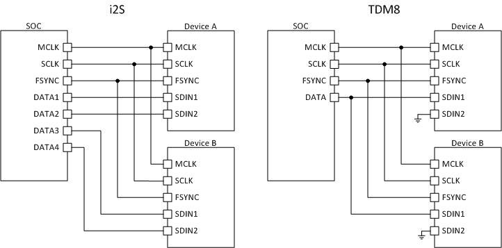
GUID-C7A92EA4-5C91-4BEA-82E9-F25A876ED182-low.gif Figure 9-1 Digital-Audio Data Connection