JAJST56D October 2001 – February 2024 TFP410
PRODUCTION DATA
- 1
- 1 特長
- 2 アプリケーション
- 3 概要
- 4 Pin Configuration and Functions
- 5 Specifications
-
6 Detailed Description
- 6.1 Overview
- 6.2 Functional Block Diagram
- 6.3 Feature Description
- 6.4 Device Functional Modes
- 6.5 Programming
- 6.6
Register Maps
- 6.6.1 VEN_ID Register (Sub-Address = 01−00 ) [reset = 0x014C]
- 6.6.2 DEV_ID Register (Sub-Address = 03–02) [reset = 0x0410]
- 6.6.3 REV_ID Register (Sub-Address = 04) [reset = 0x00]
- 6.6.4 Reserved Register (Sub-Address = 07–05) [reset = 0x641400]
- 6.6.5 CTL_1_MODE (Sub-Address = 08) [reset = 0xBE]
- 6.6.6 CTL_2_MODE Register (Sub-Address = 09) [reset = 0x00]
- 6.6.7 CTL_3_MODE Register (Sub-Address = 0A) [reset = 0x80]
- 6.6.8 CFG Register (Sub-Address = 0B)
- 6.6.9 RESERVED Register (Sub-Address = 0E–0C) [reset = 0x97D0A9]
- 6.6.10 DE_DLY Register (Sub-Address = 32) [reset = 0x00]
- 6.6.11 DE_CTL Register (Sub-Address = 33) [reset = 0x00]
- 6.6.12 DE_TOP Register (Sub-Address = 34) [reset = 0x00]
- 6.6.13 DE_CNT Register (Sub-Address = 37–36) [reset = 0x0000]
- 6.6.14 DE_LIN Register (Sub-Address = 39–38) [reset = 0x0000]
- 6.6.15 H_RES Register (Sub-Address = 3B−3A)
- 6.6.16 V_RES Register (Sub-Address = 3D−3C)
- 7 Application and Implementation
- 8 Device and Documentation Support
- 9 Revision History
- 10Mechanical, Packaging, and Orderable Information
パッケージ・オプション
デバイスごとのパッケージ図は、PDF版データシートをご参照ください。
メカニカル・データ(パッケージ|ピン)
- PAP|64
サーマルパッド・メカニカル・データ
- PAP|64
発注情報
6.4.2 Data De-skew Feature
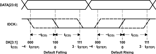
The de-skew feature allows adjustment of the input setup/hold time. Specifically, the input data DATA[23:0] can be latched slightly before or after the latching edge of the clock IDCK± depending on the amount of de-skew desired. When de-skew enable (DKEN) is enabled, the amount of de-skew is programmable by setting the three bits DK[3:1]. When disabled, a default de-skew setting is used. To allow maximum flexibility and ease of use, DKEN and DK[3:1] are accessed directly through configuration pins when I2C is disabled, or through registers of the same name when I2C is enabled. When using I2C mode, the DKEN pin should be tied to ground to avoid a floating input.
The input setup/hold time can be varied with respect to the input clock by an amount t(CD) given by the formula in Equation 1.
where
- t(STEP) is the adjustment increment amount
- DK[3:1] is a number from 0 to 7 represented as a 3-bit binary number
- t(CD) is the cumulative de-skew amount
(DK[3:1]-4) is simply a multiplier in the range {-4,-3,-2,-1, 0, 1, 2, 3} for t(STEP). Therefore, data can be latched in increments from 4 times the value of t(STEP) before the latching edge of the clock to 3 times the value of t(STEP) after the latching edge. Note that the input clock is not changed, only the time when data is latched with respect to the clock.
 Figure 6-3 A Graphical Representation of the De-Skew Function