JAJSL64D April 2016 – June 2021 THS4551
PRODUCTION DATA
- 1 特長
- 2 アプリケーション
- 3 概要
- 4 Revision History
- 5 Companion Devices
- 6 Pin Configuration and Functions
-
7 Specifications
- 7.1 Absolute Maximum Ratings
- 7.2 ESD Ratings
- 7.3 Recommended Operating Conditions
- 7.4 Thermal Information
- 7.5 Electrical Characteristics: (VS+) – (VS–) = 5 V
- 7.6 Electrical Characteristics: (VS+) – (VS–) = 3 V
- 7.7 Typical Characteristics: (VS+) – (VS–) = 5 V
- 7.8 Typical Characteristics: (VS+) – (VS–) = 3 V
- 7.9 Typical Characteristics: 3-V to 5-V Supply Range
-
8 Parameter Measurement Information
- 8.1 Example Characterization Circuits
- 8.2 Output Interface Circuit for DC-Coupled Differential Testing
- 8.3 Output Common-Mode Measurements
- 8.4 Differential Amplifier Noise Measurements
- 8.5 Balanced Split-Supply Versus Single-Supply Characterization
- 8.6 Simulated Characterization Curves
- 8.7 Terminology and Application Assumptions
- 9 Detailed Description
- 10Application and Implementation
- 11Power Supply Recommendations
- 12Layout
- 13Device and Documentation Support
- 14Mechanical, Packaging, and Orderable Information
パッケージ・オプション
メカニカル・データ(パッケージ|ピン)
サーマルパッド・メカニカル・データ
発注情報
10.1.4 Interfacing to High-Performance Precision ADCs
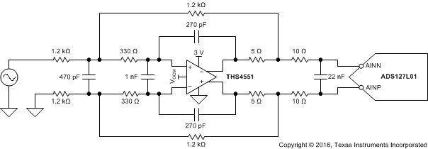
The THS4551 provides a simple interface to a wide variety of precision SAR and delta-sigma (ΔΣ) ADCs. To deliver the exceptional distortion at the output pins, considerably wider bandwidth than what is typically required in the signal path to the ADC inputs is provided by the THS4551. This wide amplifier bandwidth provides the low broadband, closed-loop output impedance to supply the sampling glitches and to recover quickly for the best SFDR. A particularly challenging task is to drive the high-frequency modulator sample rates for a precision ΔΣ converter where the modulator frequency can be far higher than the final output data rate. Figure 10-2 shows a tested example circuit using the THS4551 in a 500-kHz, active multiple feedback (MFB) filter driving the 24-bit ADS127L01. This filter is designed for FO = 500 kHz and Q = 0.63 to give a linear phase response with the –3-dB frequency at 443 kHz. This example circuit is available as a TINA-TI™ simulation file.
 Figure 10-2 500-kHz Low-Pass Active Filter
This 3-V supply example provides a low-power interface to the very low-power ADC. This circuit is available on the ADS127L01EVM board.
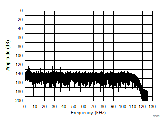
The 5-Ω resistors inside the loop at the output pins and the 1-nF differential capacitor across the FDA input pins are not part of the filter design. These elements function to improve the loop-phase margin with minimal interaction with the active filter operation To observe the loop gain and phase margin, use the SBOC461 TINA-TI™ simulation file. Tested performance with the ADS127L01 at a 4-kHz input shows the exceptional THD and SNR of –114 dBc and 106 dB, respectively. Figure 10-3 uses the ADS127L01 at a modulator frequency of 16 MHz.
 Figure 10-3 4-kHz FFT Test for the Gain of 1 V/V Interface in Figure 10-2