JAJSDF4A May 2017 – May 2019 TMP116
PRODUCTION DATA.
- 1 特長
- 2 アプリケーション
- 3 概要
- 4 改訂履歴
- 5 Pin Configuration and Functions
- 6 Specifications
-
7 Detailed Description
- 7.1 Overview
- 7.2 Functional Block Diagrams
- 7.3 Feature Description
- 7.4 Device Functional Modes
- 7.5
Programming
- 7.5.1 EEPROM Programming
- 7.5.2 Pointer Register
- 7.5.3 I2C and SMBus Interface
- 7.6
Registers Map
- 7.6.1
Register Descriptions
- 7.6.1.1 Temperature Register (address = 00h) [default reset = 8000h]
- 7.6.1.2 Configuration Register (address = 01h) [Factory default reset = 0220h]
- 7.6.1.3 High Limit Register (address = 02h) [Factory default reset = 6000h]
- 7.6.1.4 Low Limit Register (address = 03h) [Factory default reset = 8000h]
- 7.6.1.5 EEPROM Unlock Register (address = 04h) [reset = 0000h]
- 7.6.1.6 EEPROM1 Register (address = 05h) [reset = XXXXh]
- 7.6.1.7 EEPROM2 Register (address = 06h) [reset = XXXXh]
- 7.6.1.8 EEPROM3 Register (address = 07h) [reset = 0000h]
- 7.6.1.9 EEPROM4 Register (address = 08h) [reset = XXXXh]
- 7.6.1.10 Device ID Register (address = 0Fh) [reset = 1116h]
- 7.6.1
Register Descriptions
- 8 Application and Implementation
- 9 Power Supply Recommendations
- 10Layout
- 11デバイスおよびドキュメントのサポート
- 12メカニカル、パッケージ、および注文情報
パッケージ・オプション
メカニカル・データ(パッケージ|ピン)
- DRV|6
サーマルパッド・メカニカル・データ
- DRV|6
発注情報
7.4.1.2 Averaging
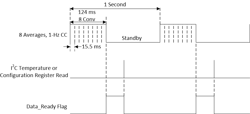
Noise in the conversion result can be reduced by configuring the device to report the average of multiple temperature conversions using the AVG[1:0] bits. When the TMP116 is configured to perform averaging, the device executes the configured number of conversions while accumulating the results and reports the average of all conversion results at the end of the process. As illustrated in the noise histograms of Figure 6 and Figure 7, the temperature result output has a repeatability of approximately ±3 LSBs when there is no averaging and ±1 LSB when the device is configured to perform eight averages or higher. As illustrated in Figure 20, this improvement in noise performance is achieved with the tradeoff of an increase in the active conversion time in a conversion cycle, thereby increasing the average active current consumption. For example, a single active conversion typically takes 15.5 ms so if the device is configured to report an average of eight conversions then the active conversion time is 124 ms (15.5 ms × 8). Use Equation 1 to factor in this increase in active conversion time to accurately calculate the average current consumption of the device. The average current consumption of the device can be decreased by increasing the amount of time the device spends in standby period as compared to active conversion. Under the factory EEPROM settings, the device is configured to report an average of eight conversions with a conversion cycle time of 1 second.
 Figure 20. Averaging Timing Diagram
 Use Equation 1 to calculate the average current consumption of the device in continuous mode.
