JAJSDF4A May 2017 – May 2019 TMP116
PRODUCTION DATA.
- 1 特長
- 2 アプリケーション
- 3 概要
- 4 改訂履歴
- 5 Pin Configuration and Functions
- 6 Specifications
-
7 Detailed Description
- 7.1 Overview
- 7.2 Functional Block Diagrams
- 7.3 Feature Description
- 7.4 Device Functional Modes
- 7.5
Programming
- 7.5.1 EEPROM Programming
- 7.5.2 Pointer Register
- 7.5.3 I2C and SMBus Interface
- 7.6
Registers Map
- 7.6.1
Register Descriptions
- 7.6.1.1 Temperature Register (address = 00h) [default reset = 8000h]
- 7.6.1.2 Configuration Register (address = 01h) [Factory default reset = 0220h]
- 7.6.1.3 High Limit Register (address = 02h) [Factory default reset = 6000h]
- 7.6.1.4 Low Limit Register (address = 03h) [Factory default reset = 8000h]
- 7.6.1.5 EEPROM Unlock Register (address = 04h) [reset = 0000h]
- 7.6.1.6 EEPROM1 Register (address = 05h) [reset = XXXXh]
- 7.6.1.7 EEPROM2 Register (address = 06h) [reset = XXXXh]
- 7.6.1.8 EEPROM3 Register (address = 07h) [reset = 0000h]
- 7.6.1.9 EEPROM4 Register (address = 08h) [reset = XXXXh]
- 7.6.1.10 Device ID Register (address = 0Fh) [reset = 1116h]
- 7.6.1
Register Descriptions
- 8 Application and Implementation
- 9 Power Supply Recommendations
- 10Layout
- 11デバイスおよびドキュメントのサポート
- 12メカニカル、パッケージ、および注文情報
パッケージ・オプション
メカニカル・データ(パッケージ|ピン)
- DRV|6
サーマルパッド・メカニカル・データ
- DRV|6
発注情報
7.5.3.1.8 Timing Diagrams
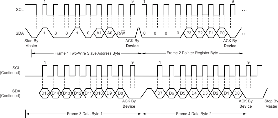
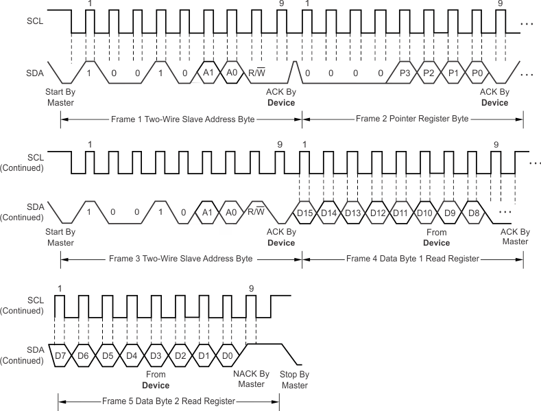
The TMP116 is two-wire, SMBus, and I2C interface-compatible. Figure 27 to Figure 30 describe the various operations on the TMP116. Parameters for Figure 1 are defined in Two-Wire Interface Timing. Bus definitions are:
Bus Idle: Both SDA and SCL lines remain high.
Start Data Transfer: A change in the state of the SDA line from high to low when the SCL line is high defines a START condition. Each data transfer is initiated with a START condition.
Stop Data Transfer: A change in the state of the SDA line from low to high when the SCL line is high defines a STOP condition. Each data transfer is terminated with a repeated START or STOP condition.
Data Transfer: The number of data bytes transferred between a START and a STOP condition is not limited and is determined by the master device.
Acknowledge: Each receiving device, when addressed, is obliged to generate an acknowledge bit. A device that acknowledges must pull down the SDA line during the acknowledge clock pulse in such a way that the SDA line is stable low during the high period of the acknowledge clock pulse. Setup and hold times must be taken into account. On a master receive, the termination of the data transfer can be signaled by the master generating a not-acknowledge (1) on the last byte transmitted by the slave.
 Figure 27. Write Word Command Timing Diagram
  Figure 28. Read Word Command Timing Diagram
  Figure 29. SMBus ALERT Timing Diagram
  Figure 30. General-Call Reset Command Timing Diagram