JAJSDF4A May 2017 – May 2019 TMP116
PRODUCTION DATA.
- 1 特長
- 2 アプリケーション
- 3 概要
- 4 改訂履歴
- 5 Pin Configuration and Functions
- 6 Specifications
-
7 Detailed Description
- 7.1 Overview
- 7.2 Functional Block Diagrams
- 7.3 Feature Description
- 7.4 Device Functional Modes
- 7.5
Programming
- 7.5.1 EEPROM Programming
- 7.5.2 Pointer Register
- 7.5.3 I2C and SMBus Interface
- 7.6
Registers Map
- 7.6.1
Register Descriptions
- 7.6.1.1 Temperature Register (address = 00h) [default reset = 8000h]
- 7.6.1.2 Configuration Register (address = 01h) [Factory default reset = 0220h]
- 7.6.1.3 High Limit Register (address = 02h) [Factory default reset = 6000h]
- 7.6.1.4 Low Limit Register (address = 03h) [Factory default reset = 8000h]
- 7.6.1.5 EEPROM Unlock Register (address = 04h) [reset = 0000h]
- 7.6.1.6 EEPROM1 Register (address = 05h) [reset = XXXXh]
- 7.6.1.7 EEPROM2 Register (address = 06h) [reset = XXXXh]
- 7.6.1.8 EEPROM3 Register (address = 07h) [reset = 0000h]
- 7.6.1.9 EEPROM4 Register (address = 08h) [reset = XXXXh]
- 7.6.1.10 Device ID Register (address = 0Fh) [reset = 1116h]
- 7.6.1
Register Descriptions
- 8 Application and Implementation
- 9 Power Supply Recommendations
- 10Layout
- 11デバイスおよびドキュメントのサポート
- 12メカニカル、パッケージ、および注文情報
パッケージ・オプション
メカニカル・データ(パッケージ|ピン)
- DRV|6
サーマルパッド・メカニカル・データ
- DRV|6
発注情報
7.4.2.1 Alert Mode
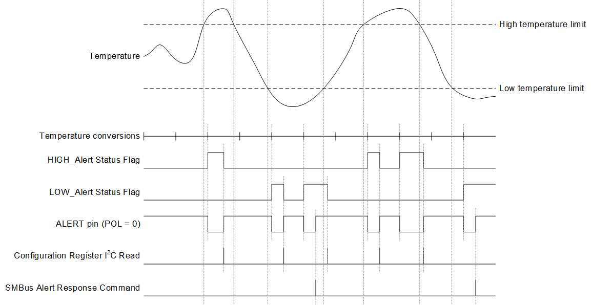
When the T/nA bit in the configuration register is set to 0, the device is in alert mode. In this mode, the device compares the conversion result at the end of every conversion with the values in the low limit register and high limit register. If the temperature result exceeds the value in the high limit register, the HIGH_Alert status flag in the configuration register is set. On the other hand, if the temperature result is lower than the value in the low limit register, the LOW_Alert status flag in the configuration register is set. As shown in Figure 23, in alert mode the status flags can be cleared by performing an I2C read of the configuration register.
Configuring the device in alert mode also affects the behaviour of the ALERT pin. In this mode, the device asserts the ALERT pin when either the HIGH_Alert or the LOW_Alert status flag is set as shown in Figure 23. The ALERT pin can be deasserted by either performing an I2C read of the configuration register (which also clears the status flags) or by performing an SMBus alert response command (see the SMBus Alert Function section). The polarity of the ALERT pin can be changed by using the POL bit setting in the configuration register.
This mode effectively makes the device behave like a window limit detector and can be used in applications where detecting if the temperature goes outside of the specified range is needed.
 Figure 23. Alert Mode Timing Diagram