JAJSHU2A August 2019 – July 2020 TMUX1208-Q1
PRODUCTION DATA
- 1 特長
- 2 アプリケーション
- 3 概要
- 4 Revision History
- 5 Pin Configuration and Functions
-
6 Specifications
- 6.1 Absolute Maximum Ratings
- 6.2 ESD Ratings
- 6.3 Recommended Operating Conditions
- 6.4 Thermal Information
- 6.5 Electrical Characteristics (VDD = 5 V ±10 %)
- 6.6 Electrical Characteristics (VDD = 3.3 V ±10 %)
- 6.7 Electrical Characteristics (VDD = 1.8 V ±10 %)
- 6.8 Electrical Characteristics (VDD = 1.2 V ±10 %)
- 7 Parameter Measurement Information
- 8 Detailed Description
- 9 Power Supply Recommendations
- 10Layout
- 11Device and Documentation Support
- 12Electrostatic Discharge Caution
- 13Glossary
7.6 tON(EN) and tOFF(EN)
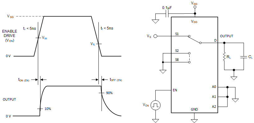
Turn-on time is defined as the time taken by the output of the device to rise to 10% after the enable has risen past the logic threshold. The 10% measurement is utilized to provide the timing of the device, system level timing can then account for the time constant added from the load resistance and load capacitance. Figure 7-6 shows the setup used to measure transition time, denoted by the symbol tON(EN).
Turn-off time is defined as the time taken by the output of the device to fall to 90% after the enable has fallen past the logic threshold. The 90% measurement is utilized to provide the timing of the device, system level timing can then account for the time constant added from the load resistance and load capacitance. Figure 7-6 shows the setup used to measure transition time, denoted by the symbol tOFF(EN).
 Figure 7-6 Turn-On and Turn-Off Time Measurement Setup