JAJSJ15B October 2020 – March 2022 TPS25947
PRODUCTION DATA
- 1 特長
- 2 アプリケーション
- 3 概要
- 4 Revision History
- 5 Device Comparison Table
- 6 Pin Configuration and Functions
- 7 Specifications
-
8 Detailed Description
- 8.1 Overview
- 8.2 Functional Block Diagram
- 8.3
Feature Description
- 8.3.1 Input Reverse Polarity Protection
- 8.3.2 Undervoltage Lockout (UVLO and UVP)
- 8.3.3 Overvoltage Lockout (OVLO)
- 8.3.4 Overvoltage Clamp (OVC)
- 8.3.5 Inrush Current, Overcurrent, and Short Circuit Protection
- 8.3.6 Analog Load Current Monitor
- 8.3.7 Reverse Current Protection
- 8.3.8 Overtemperature Protection (OTP)
- 8.3.9 Fault Response and Indication (FLT)
- 8.3.10 Auxiliary Channel Control (AUXOFF)
- 8.3.11 Power Good Indication (PG)
- 8.4 Device Functional Modes
- 9 Application and Implementation
- 10Power Supply Recommendations
- 11Layout
- 12Device and Documentation Support
- 13Mechanical, Packaging, and Orderable Information
9.6 USB PD Port Protection
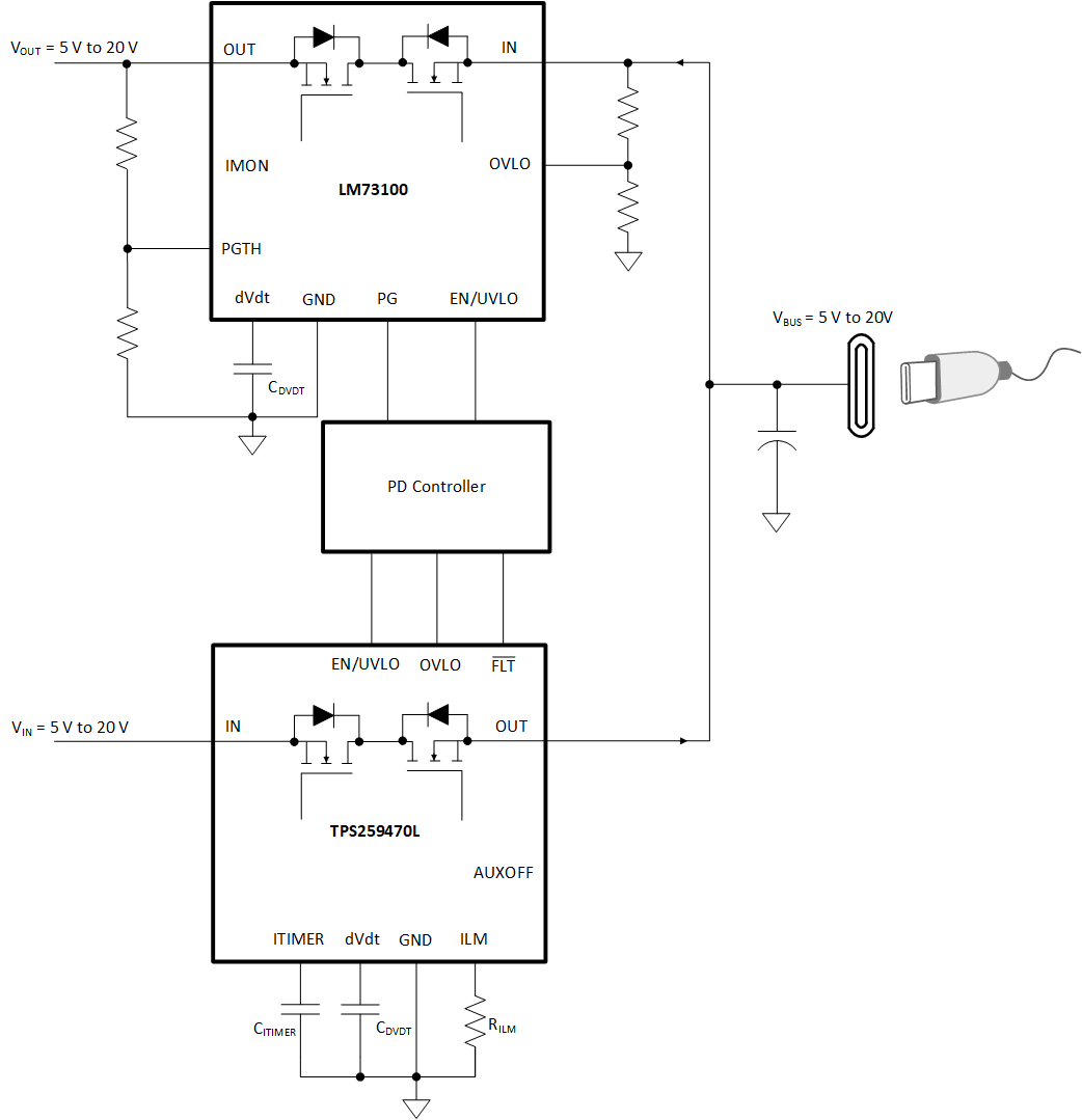
End equipments like PC, Notebooks, Docking Stations, Monitors etc.. have USB PD ports which can be configured as DFP (Source), UFP (Sink) or DRP (Source+Sink). TPS259470x can be used independently or in conjunction with LM73100 to handle the power path protection requirements of USB PD ports as shown in Figure 9-16 below.
TPS259470x provides Overcurrent and Short-Circuit protection in the source path, while blocking any reverse current from the port to the internal source power rail. The fast recovery (tSWRCB) from reverse current blocking ensures minimum supply droop during Fast Role Swap (FRS) events. The PD controller can also use the OVLO pin as an active low enable signal to control the power path. Holding the OVLO pin high keeps the device in OFF state in sink mode and blocks current in both directions. After the PD controller determines the need to start sourcing power, it can pull the OVLO pin low to trigger a fast recovery from OFF to ON state within tSWOV, meeting the FRS timing requirements.
The LM73100 provides overvoltage protection on the sink path, while blocking reverse current from internal sink rail to the port.
The linear ORing mechanism in TPS259470x and LM73100 ensures that there's no reverse current flowing from one power source to the other during fast or slow ramp of either supply.
 Figure 9-16 USB PD Port Protection
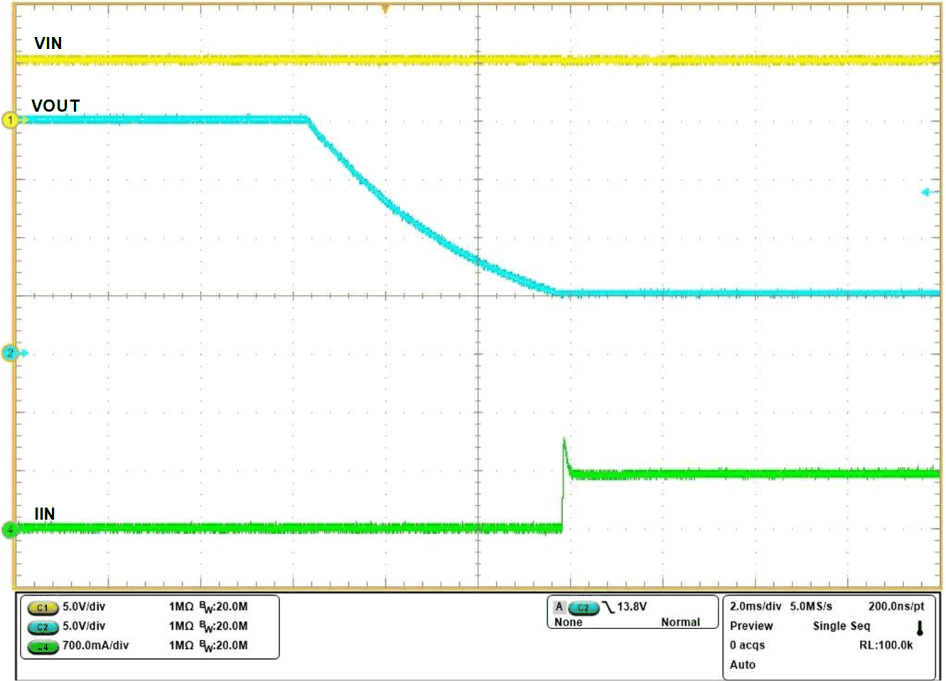
The waveform below shows the TPS259470x behavior when a 20-V source connected at the USB bus is suddenly disconnected. The TPS259470x is initially in reverse current blocking condition. As the bus voltage starts drooping, the TPS259470x exits the condition and performs a fast charge to restore the bus voltage above vSafe5V(min) within tSWRCB, thereby meeting the USB FRS (Fast Role Swap) requirements.

| VIN = 5 V, COUT = 10 μF, ROUT = 8 Ω, VOUT = 20 V initially and then disconnected |