JAJSJ15B October 2020 – March 2022 TPS25947
PRODUCTION DATA
- 1 特長
- 2 アプリケーション
- 3 概要
- 4 Revision History
- 5 Device Comparison Table
- 6 Pin Configuration and Functions
- 7 Specifications
-
8 Detailed Description
- 8.1 Overview
- 8.2 Functional Block Diagram
- 8.3
Feature Description
- 8.3.1 Input Reverse Polarity Protection
- 8.3.2 Undervoltage Lockout (UVLO and UVP)
- 8.3.3 Overvoltage Lockout (OVLO)
- 8.3.4 Overvoltage Clamp (OVC)
- 8.3.5 Inrush Current, Overcurrent, and Short Circuit Protection
- 8.3.6 Analog Load Current Monitor
- 8.3.7 Reverse Current Protection
- 8.3.8 Overtemperature Protection (OTP)
- 8.3.9 Fault Response and Indication (FLT)
- 8.3.10 Auxiliary Channel Control (AUXOFF)
- 8.3.11 Power Good Indication (PG)
- 8.4 Device Functional Modes
- 9 Application and Implementation
- 10Power Supply Recommendations
- 11Layout
- 12Device and Documentation Support
- 13Mechanical, Packaging, and Orderable Information
10.1 Transient Protection
In the case of a short-circuit and overload current limit when the device interrupts current flow, the input inductance generates a positive voltage spike on the input, and the output inductance generates a negative voltage spike on the output. The peak amplitude of voltage spikes (transients) is dependent on the value of inductance in series to the input or output of the device. Such transients can exceed the absolute maximum ratings of the device if steps are not taken to address the issue. Typical methods for addressing transients include:
- Minimize lead length and inductance into and out of the device.
- Use a large PCB GND plane.
- Connect a Schottky diode from the OUT pin ground to absorb negative spikes.
- Connect a low ESR capacitor larger than 1 μF at the OUT pin very close to the device.
- Use a low-value ceramic capacitor
CIN = 1 μF to absorb the energy and dampen the transients. The capacitor
voltage rating must be atleast twice the input supply voltage to be able to withstand
the positive voltage excursion during inductive ringing.
The approximate value of input capacitance can be estimated with Equation 24:
Equation 24.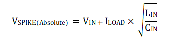
where
- VIN is the nominal supply voltage.
- • ILOAD is the load current.
- LIN equals the effective inductance seen looking into the source.
- CIN is the capacitance present at the input.
- Some applications can require the
addition of a Transient Voltage Suppressor (TVS) to prevent transients from exceeding the
absolute maximum ratings of the device. In some cases, even if the maximum amplitude of
the transients is below the absolute maximum rating of the device, a TVS can help to
absorb the excessive energy dump and prevent it from creating very fast transient voltages
on the input supply pin of the IC, which can couple to the internal control circuits and
cause unexpected behavior. Note: If there is a likelihood of input reverse polarity in the system, TI recommends to use a bi-directional TVS, or a reverse blocking diode in series with the TVS.
- For applications such as USB-C ports where a powered cable can be plugged to the output of the device, there can be excess voltage stress from OUT to IN which exceeds the absolute maximum rating of the device. TI recommends to add a TVS diode from OUT to IN to clamp the voltage to a safe level.
The circuit implementation with optional protection components is shown in Figure 10-1.
 Figure 10-1 Circuit Implementation with Optional
Protection Components
Figure 10-1 Circuit Implementation with Optional
Protection Components