JAJSJ15B October   2020  – March 2022 TPS25947

PRODUCTION DATA  

  1. 特長
  2. アプリケーション
  3. 概要
  4. Revision History
  5. Device Comparison Table
  6. Pin Configuration and Functions
  7. Specifications
    1. 7.1 Absolute Maximum Ratings
    2. 7.2 ESD Ratings
    3. 7.3 Recommended Operating Conditions
    4. 7.4 Thermal Information
    5. 7.5 Electrical Characteristics
    6. 7.6 Timing Requirements
    7. 7.7 Switching Characteristics
      1.      15
    8. 7.8 Typical Characteristics
  8. Detailed Description
    1. 8.1 Overview
    2. 8.2 Functional Block Diagram
    3. 8.3 Feature Description
      1. 8.3.1  Input Reverse Polarity Protection
      2. 8.3.2  Undervoltage Lockout (UVLO and UVP)
      3. 8.3.3  Overvoltage Lockout (OVLO)
      4. 8.3.4  Overvoltage Clamp (OVC)
      5. 8.3.5  Inrush Current, Overcurrent, and Short Circuit Protection
        1. 8.3.5.1 Slew Rate (dVdt) and Inrush Current Control
        2. 8.3.5.2 Circuit-Breaker
        3. 8.3.5.3 Active Current Limiting
        4. 8.3.5.4 Short-Circuit Protection
      6. 8.3.6  Analog Load Current Monitor
      7. 8.3.7  Reverse Current Protection
      8. 8.3.8  Overtemperature Protection (OTP)
      9. 8.3.9  Fault Response and Indication (FLT)
      10. 8.3.10 Auxiliary Channel Control (AUXOFF)
      11. 8.3.11 Power Good Indication (PG)
    4. 8.4 Device Functional Modes
  9. Application and Implementation
    1. 9.1 Application Information
    2. 9.2 Single Device, Self-Controlled
    3. 9.3 Typical Application
      1. 9.3.1 Design Requirements
      2. 9.3.2 Detailed Design Procedure
        1. 9.3.2.1 Device Selection
        2. 9.3.2.2 Setting Undervoltage and Overvoltage Thresholds
        3. 9.3.2.3 Setting Output Voltage Rise Time (tR)
        4. 9.3.2.4 Setting Power Good Assertion Threshold
        5. 9.3.2.5 Setting Overcurrent Threshold (ILIM)
        6. 9.3.2.6 Setting Overcurrent Blanking Interval (tITIMER)
      3. 9.3.3 Application Curves
    4. 9.4 Active ORing
    5. 9.5 Priority Power MUXing
    6. 9.6 USB PD Port Protection
    7. 9.7 Parallel Operation
  10. 10Power Supply Recommendations
    1. 10.1 Transient Protection
    2. 10.2 Output Short-Circuit Measurements
  11. 11Layout
    1. 11.1 Layout Guidelines
    2. 11.2 Layout Example
  12. 12Device and Documentation Support
    1. 12.1 Documentation Support
      1. 12.1.1 Related Documentation
    2. 12.2 Receiving Notification of Documentation Updates
    3. 12.3 サポート・リソース
    4. 12.4 Trademarks
    5. 12.5 Electrostatic Discharge Caution
    6. 12.6 Glossary
  13. 13Mechanical, Packaging, and Orderable Information

パッケージ・オプション

メカニカル・データ(パッケージ|ピン)
サーマルパッド・メカニカル・データ
発注情報

Setting Undervoltage and Overvoltage Thresholds

The supply undervoltage and overvoltage thresholds are set using the resistors R1, R2 and R3 whose values can be calculated using Equation 10 and Equation 11:

Equation 10. GUID-20210329-CA0I-SLTM-KVB2-FD1KKD8JLFJS-low.gif
Equation 11.
Where VUVLO(R) is the UVLO rising threshold and VOV(R) is the OVLO rising threshold. Because R1, R2 and R3 leak the current from input supply VIN, these resistors must be selected based on the acceptable leakage current from input power supply VIN. The current drawn by R1, R2 and R3 from the power supply is IR123 = VIN / (R1 + R2 + R3). However, leakage currents due to external active components connected to the resistor string can add error to these calculations. So, the resistor string current, IR123 must be chosen to be 20 times greater than the leakage current expected on the EN/UVLO and OVLO pins.

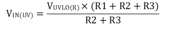
From the device electrical specifications, both the EN/UVLO and OVLO leakage currents are 0.1 μA (maximum), VOV(R) = 1.2 V and VUVLO(R) = 1.2 V. From design requirements, VIN(OV) = 13.2 V and VIN(UV) = 10.8 V. To solve the equation, first choose the value of R1 = 470 kΩ and use the above equations to solve for R2 = 10.7 kΩ and R3 = 48 kΩ.

Using the closest standard 1% resistor values, we get R1 = 470 kΩ, R2 = 11 kΩ, and R3 = 47 kΩ.