JAJSQU2A August 2023 – October 2023 TPS25983
PRODUCTION DATA
- 1
- 1 特長
- 2 アプリケーション
- 3 概要
- 4 Revision History
- 5 Device Comparison Table
- 6 Pin Configuration and Functions
- 7 Specifications
-
8 Detailed Description
- 8.1 Overview
- 8.2 Functional Block Diagram
- 8.3
Feature Description
- 8.3.1 Undervoltage Protection (UVLO and UVP)
- 8.3.2 Overvoltage Protection (OVP)
- 8.3.3 Inrush Current, Overcurrent, and Short-Circuit Protection
- 8.3.4 Overtemperature Protection (OTP)
- 8.3.5 Analog Load Current Monitor (IMON)
- 8.3.6 Power Good (PG)
- 8.3.7 Reverse Current Blocking FET Driver
- 8.3.8 Fault Response
- 8.4 Device Functional Modes
-
9 Application and Implementation
- 9.1 Application Information
- 9.2
Typical Application: Standby Power Rail Protection in Datacenter Servers
- 9.2.1 Design Requirements
- 9.2.2
Detailed Design Procedure
- 9.2.2.1 Device Selection
- 9.2.2.2 Setting the Current Limit Threshold: RILIM Selection
- 9.2.2.3 Setting the Undervoltage and Overvoltage Lockout Set Point
- 9.2.2.4 Choosing the Current Monitoring Resistor: RIMON
- 9.2.2.5 Setting the Output Voltage Ramp Time (TdVdt)
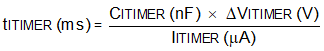
- 9.2.2.6 Setting the Transient Overcurrent Blanking Interval (tITIMER)
- 9.2.2.7 Setting the Auto-Retry Delay and Number of Retries
- 9.2.3 Application Curves
- 9.3 System Examples
- 9.4 Power Supply Recommendations
- 9.5 Layout
- 10Device and Documentation Support
- 11Mechanical, Packaging, and Orderable Information
パッケージ・オプション
メカニカル・データ(パッケージ|ピン)
- RGE|24
サーマルパッド・メカニカル・データ
- RGE|24
発注情報
8.3.3.3 Active Current Limiting
The TPS25983xL (Current Limiter) variants respond to output overcurrent conditions by actively regulating the current to a set limit after a user adjustable fault blanking interval. During steady-state operation, if the load current exceeds a user adjustable overcurrent threshold (ILIM) set by the ILIM pin resistor (RILIM), but lower than the fast-trip threshold (IFT), the device starts discharging the ITIMER pin capacitor using an internal pull-down current (IITIMER). If the load current drops below the overcurrent threshold before the ITIMER capacitor voltage drops by ΔVITIMER, the current limit action is not engaged and the ITIMER is reset by pulling it up to VINT internally. This allows short transient overcurrent pulses to pass through the device without limiting the current. If the overcurrent condition persists, the ITIMER capacitor continues to discharge and once it falls by ΔVITIMER, the device regulates the FET gate voltage to actively limit the output current to the set ILIM level. The device will exit current limiting when the load current falls below ILIM. Equation 7 can be used to calculate the RILIM value for a desired current limit.
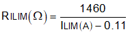
Leaving the ILIM pin Open sets the overcurrent threshold to zero and causes the FET to shut off as soon as any load current is detected. Shorting the ILIM pin to ground at any point during normal operation is detected as a fault and the part shuts down. The ILIM pin Short to GND fault detection circuit doesn't allow any load current higher than ICB to flow through the device. This ensures robust eFuse behavior even under single point failure conditions. Refer to the Fault Response section for details on the device behavior after a fault.
 Figure 8-5 Active Current Limiter
Response
Figure 8-5 Active Current Limiter
ResponseThe duration for which load transients are allowed can be adjusted using an appropriate capacitor value from ITIMER pin to ground. The transient overcurrent blanking interval can be calculated using Equation 8.
Leave the ITIMER pin open to allow the part to activate the current limit with the minimum possible delay. Refer to ITIMER Functional Mode Summary for more details.
1. Current limiting based on RILIM is active during startup for both Current Limit and Circuit Breaker variants. In case the startup current exceeds ILIM, the device regulates the current to the set limit. However, during startup the current limit is engaged without waiting for the ITIMER delay.
2. The active current limit block employs a foldback mechanism during start-up based on the output voltage (VOUT). When VOUT is below the foldback threshold (VFB), the current limit threshold is further lowered as compared to the steady-state setting.
3. Shorting the ITIMER pin to ground is detected as a fault and the part shuts down. This ensures robust eFuse behavior even in case of single point failure conditions. Refer to the Fault Response section for details on the device behavior after a fault.
4. Larger ITIMER capacitors take longer to charge during start-up and may lead to incorrect fault assertion if the ITIMER voltage is still below the pin short detection threshold after the device has reached steady state. To avoid this, it is recommended to limit the maximum ITIMER capacitor to the value suggested by the equation below.
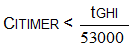
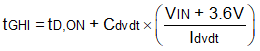
Where
- tGHI is the time taken by the device to reach steady state
- tD,ON is the device turn-on delay
- Cdvdt is the dVdt capacitance
- Idvdt is the dVdt charging current
It is possible to avoid incorrect ITIMER pin fault assertion and achieve higher ITIMER intervals if needed by increasing the dVdt capacitor value accordingly, but at the expense of higher start-up time.
During current regulation, the output voltage will drop resulting in increased device power dissipation across the FET. If the device internal temperature (TJ) exceeds the thermal shutdown threshold (TSD), the FET is turned off. See Overtemperature Protection (OTP) for more details on device response to overtemperature.