JAJSQU2A August   2023  – October 2023 TPS25983

PRODUCTION DATA  

  1.   1
  2. 特長
  3. アプリケーション
  4. 概要
  5. Revision History
  6. Device Comparison Table
  7. Pin Configuration and Functions
  8. Specifications
    1. 7.1 Absolute Maximum Ratings
    2. 7.2 ESD Ratings
    3. 7.3 Recommended Operating Conditions
    4. 7.4 Thermal Information
    5. 7.5 Electrical Characteristics
    6. 7.6 Timing Requirements
    7. 7.7 Switching Characteristics
    8. 7.8 Typical Characteristics
  9. Detailed Description
    1. 8.1 Overview
    2. 8.2 Functional Block Diagram
    3. 8.3 Feature Description
      1. 8.3.1 Undervoltage Protection (UVLO and UVP)
      2. 8.3.2 Overvoltage Protection (OVP)
      3. 8.3.3 Inrush Current, Overcurrent, and Short-Circuit Protection
        1. 8.3.3.1 Slew Rate and Inrush Current Control (dVdt)
        2. 8.3.3.2 Circuit Breaker
        3. 8.3.3.3 Active Current Limiting
        4. 8.3.3.4 Short-Circuit Protection
      4. 8.3.4 Overtemperature Protection (OTP)
      5. 8.3.5 Analog Load Current Monitor (IMON)
      6. 8.3.6 Power Good (PG)
      7. 8.3.7 Reverse Current Blocking FET Driver
      8. 8.3.8 Fault Response
    4. 8.4 Device Functional Modes
  10. Application and Implementation
    1. 9.1 Application Information
    2. 9.2 Typical Application: Standby Power Rail Protection in Datacenter Servers
      1. 9.2.1 Design Requirements
      2. 9.2.2 Detailed Design Procedure
        1. 9.2.2.1 Device Selection
        2. 9.2.2.2 Setting the Current Limit Threshold: RILIM Selection
        3. 9.2.2.3 Setting the Undervoltage and Overvoltage Lockout Set Point
        4. 9.2.2.4 Choosing the Current Monitoring Resistor: RIMON
        5. 9.2.2.5 Setting the Output Voltage Ramp Time (TdVdt)
          1. 9.2.2.5.1 Case 1: Start-Up Without Load: Only Output Capacitance COUT Draws Current
          2. 9.2.2.5.2 Case 2: Start-Up With Load: Output Capacitance COUT and Load Draw Current
        6. 9.2.2.6 Setting the Transient Overcurrent Blanking Interval (tITIMER)
        7. 9.2.2.7 Setting the Auto-Retry Delay and Number of Retries
      3. 9.2.3 Application Curves
    3. 9.3 System Examples
      1. 9.3.1 Optical Module Power Rail Path Protection
        1. 9.3.1.1 Design Requirements
        2. 9.3.1.2 Device Selection
        3. 9.3.1.3 External Component Settings
        4. 9.3.1.4 Voltage Drop
        5. 9.3.1.5 Application Curves
      2. 9.3.2 Input Protection for 12-V Rail Applications: PCIe Cards, Storage Interfaces, and DC Fans
      3. 9.3.3 Priority Power MUXing
    4. 9.4 Power Supply Recommendations
      1. 9.4.1 Transient Protection
      2. 9.4.2 Output Short-Circuit Measurements
    5. 9.5 Layout
      1. 9.5.1 Layout Guidelines
      2. 9.5.2 Layout Example
  11. 10Device and Documentation Support
    1. 10.1 Documentation Support
      1. 10.1.1 Related Documentation
    2. 10.2 ドキュメントの更新通知を受け取る方法
    3. 10.3 サポート・リソース
    4. 10.4 Trademarks
    5. 10.5 静電気放電に関する注意事項
    6. 10.6 用語集
  12. 11Mechanical, Packaging, and Orderable Information

パッケージ・オプション

メカニカル・データ(パッケージ|ピン)
サーマルパッド・メカニカル・データ
発注情報

Typical Characteristics

GUID-20231008-SS0I-B5VL-5GFH-J8DDDVPDTWCG-low.svg
Figure 7-1 ON Resistance vs Temperature
GUID-20231008-SS0I-VWJZ-NTD6-MF4FKXLNLR5K-low.svg
Figure 7-3 OVLO Pin Threshold vs Temperature
GUID-20231008-SS0I-X5LS-WKN4-Q9PPZH1C9PJT-low.svg
Figure 7-5 EN/UVLO Falling Threshold for Lowest Current Consumption
GUID-20231008-SS0I-MBWN-CGV8-BRZBBCLGDS1X-low.svg
VENUVLO = 1 V, OUT = Open
Figure 7-7 Shut-Down Current vs Temperature
GUID-20231009-SS0I-FCVQ-WZLS-NB1KTZFVQRDS-low.svg
Figure 7-9 Recommended Maximum ILIM Setting For Safe Operation vs Input Voltage
GUID-20231010-SS0I-B3NQ-Z8SB-6FR15RXRK10C-low.svg
Across Process, Voltage, Temperature Corners
Figure 7-11 Output Current Limit (ILIM) Accuracy
GUID-20231008-SS0I-0T2Z-CS6T-9VTBX1KSKBNP-low.svg
Figure 7-13 Fixed Fast-trip Threshold vs Temperature
GUID-20231008-SS0I-TJXL-532L-SXZZRGF65N60-low.svg
VIN = 0 V, IPG = 26 μA
Figure 7-15 Power Good Output Voltage (De-asserted State) vs Temperature
GUID-20231008-SS0I-HQHT-6HWL-MRZLMTQTLS2C-low.svg
Figure 7-17 ITIMER Discharge Current vs Temperature
GUID-20230808-SS0I-ZDLD-B2ZJ-WW0VQWTJKGWD-low.svg
Figure 7-19 Thermal Shutdown Plot - Steady State
GUID-67B60639-F25E-4893-8705-FE60199CCCC9-low.png
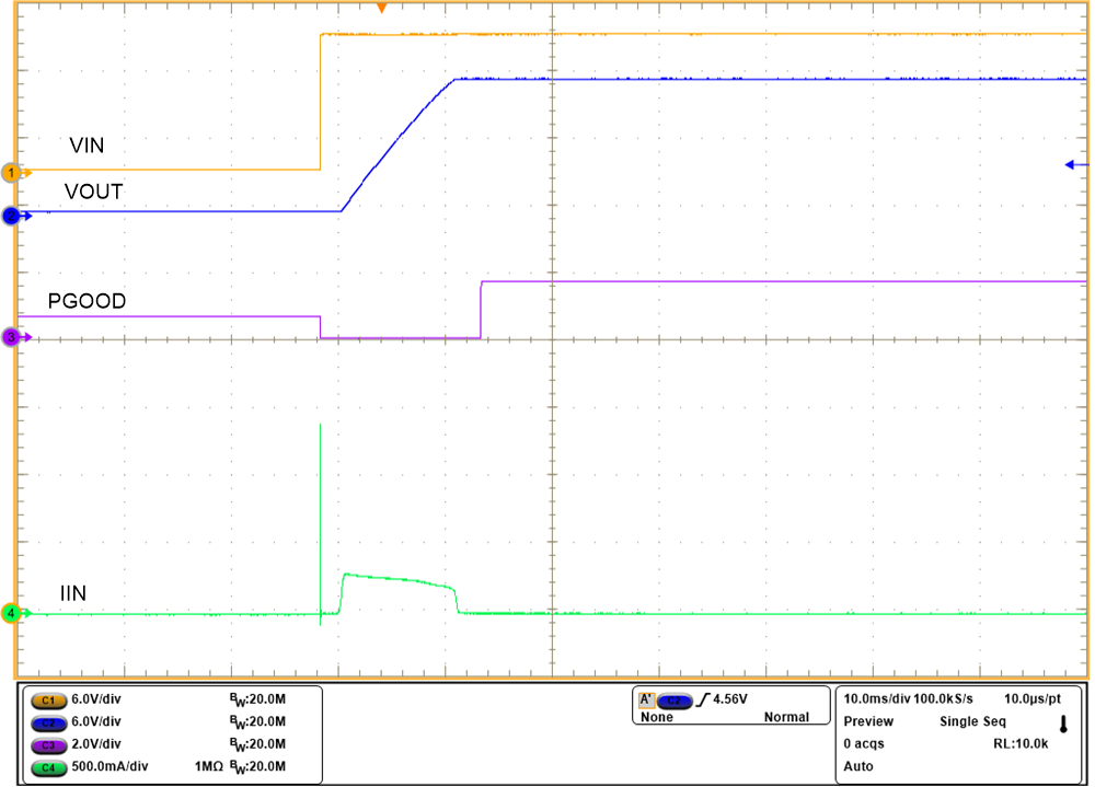
CIN = 1 μF COUT = 220 μF CdVdt = 3.3 nF
Figure 7-21 Hotplug
GUID-CFD3666B-4BBA-4635-ACF5-456B1F1994C7-low.png
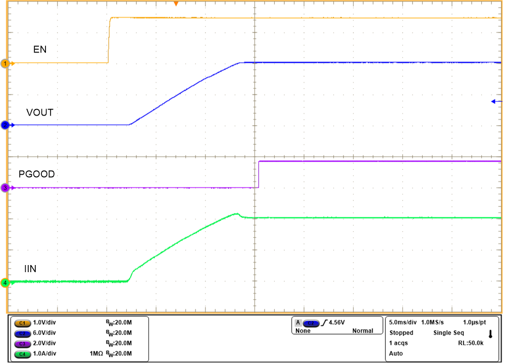
COUT = 220 μF CdVdt = 3.3 nF ROUT = 6 Ω
Figure 7-23 Start Up With EN Into Resistive Load - dVdt Limited
GUID-20230731-SS0I-MGHN-WSRH-5HG8JMJ0HTWK-low.svg
RILIM = 82 Ω CITIMER = 4.7 nF
Output load current ramped above the ILIM threshold for short duration without triggering current limit
Figure 7-25 Transient Overcurrent Blanking Timer Response
GUID-20230731-SS0I-2NTQ-B8QL-60R5QQCBXLRW-low.svg
RILIM = 82 Ω CITIMER = 4.7 nF CRETRY_DLY = 1 nF, CNRETRY = Open
Figure 7-27 Steady-state Current Limit Followed By Thermal Shutdown And Auto-Retry (TPS259830L Variant)
GUID-20230731-SS0I-SSXZ-R04W-LLVMNLLSX2X8-low.svg
RILIM = 82 Ω CITIMER = 4.7 nF CRETRY_DLY = Open, CNRETRY = Open
Figure 7-29 Steady-state Circuit Breaker Response Followed By Auto-Retry (TPS259830O Variant)
GUID-20230731-SS0I-XCDB-DQ8K-NXLCGDK4BCMJ-low.svg
RILIM = 82 Ω
Figure 7-31 Output Hard Short-Circuit During Steady-state
GUID-20230731-SS0I-TMZ4-SXNR-JVW5VHDDDSC6-low.svg
RILIM = 82 Ω
Figure 7-33 Supply Line Transient Immunity - Input Voltage Step
GUID-20231008-SS0I-X4S2-MQPT-Z1LXKJWPLK5K-low.svg
Figure 7-2 Supply UVP Threshold vs Temperature
GUID-20231008-SS0I-RV3F-NZ00-FGWZPRZVSGCQ-low.svg
Figure 7-4 EN/UVLO Pin Threshold vs Temperature
GUID-20231008-SS0I-NX8B-2132-K7PKT3SQ8VRL-low.svg
VENUVLO = 2 V, OUT = Open
Figure 7-6 Quiescent Current vs Temperature
GUID-20231008-SS0I-SDZ2-R1KK-HQHQWQLN6WLW-low.svg
VENUVLO = 0 V, OUT = Open
Figure 7-8 Deep Shut-Down Current vs Temperature
GUID-20231009-SS0I-SNVL-BKGF-KWXLSKQFSBVC-low.svg
Figure 7-10 Output Current Limit (ILIM) vs RILIM
GUID-20231010-SS0I-K71B-BXKS-QRC8CZ0MJRQZ-low.svg
Across Process, Voltage, Temperature Corners, Normalized to mean value of 243 μA/A
Figure 7-12 Output Current Monitor Gain (GIMON) Accuracy
GUID-20231009-SS0I-5JMP-QRBZ-DKHRTV2RQWGD-low.svg
VIN = 0 V, IPG = 26 μA
Figure 7-14 DVDT Pin Charging Current vs Temperature
GUID-20231008-SS0I-HBBJ-TJVN-R2CVBBXN5P4X-low.svg
Figure 7-16 ITIMER Voltage Threshold Delta vs Temperature
GUID-20231008-SS0I-VWZV-D5DD-Q3BKK21XTXWV-low.svg
Figure 7-18 ITIMER Internal Pull-up Voltage vs Temperature
GUID-20230804-SS0I-NLTS-5KJ3-F9B93WHVLDDH-low.svg
Figure 7-20 Thermal Shutdown Plot - Inrush/Overload
GUID-C5BC5F4D-9648-48C0-9AB7-FCBA208329AC-low.png
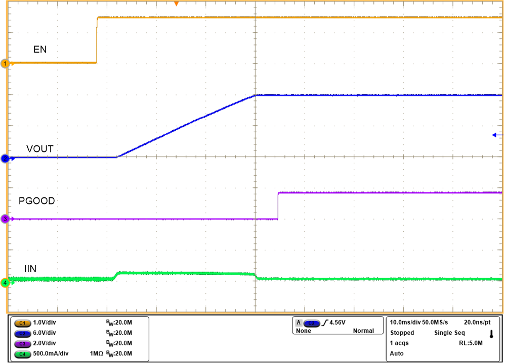
COUT = 220 μF CdVdt = 10 nF ROUT = Open
Figure 7-22 Startup With EN - dVdt Limited
GUID-20230731-SS0I-PXRW-RMKD-8PGRK1FZBZ5Z-low.svg
Figure 7-24 Overvoltage Protection
GUID-20230731-SS0I-TP9G-LMBQ-1DHQJRJMK3GS-low.svg
RILIM = 82 Ω CITIMER = 4.7 nF
Output load current ramped above the ILIM threshold beyond the ITIMER duration triggers current limit
Figure 7-26 Steady-state Current Limit Response (TPS259830L Variant)
GUID-20230731-SS0I-DTD2-GTDK-XTV9T5BGJDPZ-low.svg
RILIM = 82 Ω CITIMER = 4.7 nF
Output load current ramped above the ILIM threshold beyond the ITIMER duration triggers circuit breaker response
Figure 7-28 Steady-state Circuit Breaker Response (TPS259830O Variant)
GUID-20230731-SS0I-1VPS-B40J-HDRPMCQ83JRV-low.svg
RILIM = 82 Ω
Figure 7-30 Power Up Into Output Short-Circuit
GUID-20230731-SS0I-L6Z2-B0M0-MMVCCJW2MXPK-low.svg
RILIM = 82 Ω
Figure 7-32 Output Hard Short-Circuit During Steady-state (Zoomed In)