JAJSQU2A August 2023 – October 2023 TPS25983
PRODUCTION DATA
- 1
- 1 特長
- 2 アプリケーション
- 3 概要
- 4 Revision History
- 5 Device Comparison Table
- 6 Pin Configuration and Functions
- 7 Specifications
-
8 Detailed Description
- 8.1 Overview
- 8.2 Functional Block Diagram
- 8.3
Feature Description
- 8.3.1 Undervoltage Protection (UVLO and UVP)
- 8.3.2 Overvoltage Protection (OVP)
- 8.3.3 Inrush Current, Overcurrent, and Short-Circuit Protection
- 8.3.4 Overtemperature Protection (OTP)
- 8.3.5 Analog Load Current Monitor (IMON)
- 8.3.6 Power Good (PG)
- 8.3.7 Reverse Current Blocking FET Driver
- 8.3.8 Fault Response
- 8.4 Device Functional Modes
-
9 Application and Implementation
- 9.1 Application Information
- 9.2
Typical Application: Standby Power Rail Protection in Datacenter Servers
- 9.2.1 Design Requirements
- 9.2.2
Detailed Design Procedure
- 9.2.2.1 Device Selection
- 9.2.2.2 Setting the Current Limit Threshold: RILIM Selection
- 9.2.2.3 Setting the Undervoltage and Overvoltage Lockout Set Point
- 9.2.2.4 Choosing the Current Monitoring Resistor: RIMON
- 9.2.2.5 Setting the Output Voltage Ramp Time (TdVdt)
- 9.2.2.6 Setting the Transient Overcurrent Blanking Interval (tITIMER)
- 9.2.2.7 Setting the Auto-Retry Delay and Number of Retries
- 9.2.3 Application Curves
- 9.3 System Examples
- 9.4 Power Supply Recommendations
- 9.5 Layout
- 10Device and Documentation Support
- 11Mechanical, Packaging, and Orderable Information
パッケージ・オプション
メカニカル・データ(パッケージ|ピン)
- RGE|24
サーマルパッド・メカニカル・データ
- RGE|24
発注情報
9.2.2.5.2 Case 2: Start-Up With Load: Output Capacitance COUT and Load Draw Current
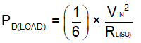
When the load draws current during the turn-on sequence, there is additional power dissipated. Considering a resistive load during start-up RL(SU), load current ramps up proportionally with increase in output voltage during TdVdt time. Equation 19 shows the average power dissipation in the internal FET during charging time due to resistive load.
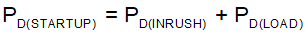
Equation 20 gives the total power dissipated in the device during start-up.
The power dissipation, with and without load, for selected start-up time must not exceed the start-up thermal shutdown limits as shown in Thermal Shutdown Plot During Start-up.
 Figure 9-2 Thermal Shutdown Plot During
Start-up
Figure 9-2 Thermal Shutdown Plot During
Start-upFor the design example under discussion, the output voltage has to be ramped up in 20 ms, which mandates a slew-rate of 0.6 V/ms for a 12-V rail.
The required CdVdt capacitance on dVdt pin to set 0.6-V/ms slew rate can be calculated using Equation 21.
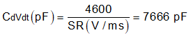
The dVdt capacitor is subjected to typically VIN + 4 V during startup. The high voltage bias leads to a drop in the effective capacitor value. So, it is suggested to choose 20% higher than the calculated value, which gives 9.2 nF. Choose closest 10% standard value: 10 nF
The 10 nF CdVdt capacitance sets a slew-rate of 0.46 V/ms and output ramp time TdVdt of 26 ms.
The inrush current drawn by the load capacitance COUT during ramp-up can be calculated using Equation 22.
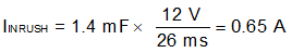
The inrush power dissipation can be calculated using Equation 23.

For 3.9 W of power loss, the thermal shutdown time of the device must be greater than the ramp-up time TdVdt to ensure a successful start-up. Figure 9-2 shows the start-up thermal shutdown limit. For 3.9 W of power, the shutdown time is approximately 100 ms. So it is safe to use 26 ms as the start-up time without any load on the output.
The additional power dissipation when a 10-Ω load is present during start-up is calculated using Equation 24.
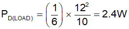
The total device power dissipation during start-up can be calculated using Equation 25.
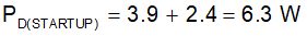
From Thermal Shutdown Plot During Start-up, the thermal shutdown time for 6.3 W is approximately 40 ms. It is safe to have 30% margin to allow for variation of system parameters such as load, component tolerance, and input voltage. So it is well within acceptable limits to use the 10 nF for CdVdt capacitor with start-up load of 10 Ω.
When COUT is large, there is a need to decrease the power dissipation during start-up. This can be done by increasing the value of the CdVdt capacitor. A spreadsheet tool TPS25983xx Design Calculator available on the web can be used for iterative calculations.