JAJSQU2A August 2023 – October 2023 TPS25983
PRODUCTION DATA
- 1
- 1 特長
- 2 アプリケーション
- 3 概要
- 4 Revision History
- 5 Device Comparison Table
- 6 Pin Configuration and Functions
- 7 Specifications
-
8 Detailed Description
- 8.1 Overview
- 8.2 Functional Block Diagram
- 8.3
Feature Description
- 8.3.1 Undervoltage Protection (UVLO and UVP)
- 8.3.2 Overvoltage Protection (OVP)
- 8.3.3 Inrush Current, Overcurrent, and Short-Circuit Protection
- 8.3.4 Overtemperature Protection (OTP)
- 8.3.5 Analog Load Current Monitor (IMON)
- 8.3.6 Power Good (PG)
- 8.3.7 Reverse Current Blocking FET Driver
- 8.3.8 Fault Response
- 8.4 Device Functional Modes
-
9 Application and Implementation
- 9.1 Application Information
- 9.2
Typical Application: Standby Power Rail Protection in Datacenter Servers
- 9.2.1 Design Requirements
- 9.2.2
Detailed Design Procedure
- 9.2.2.1 Device Selection
- 9.2.2.2 Setting the Current Limit Threshold: RILIM Selection
- 9.2.2.3 Setting the Undervoltage and Overvoltage Lockout Set Point
- 9.2.2.4 Choosing the Current Monitoring Resistor: RIMON
- 9.2.2.5 Setting the Output Voltage Ramp Time (TdVdt)
- 9.2.2.6 Setting the Transient Overcurrent Blanking Interval (tITIMER)
- 9.2.2.7 Setting the Auto-Retry Delay and Number of Retries
- 9.2.3 Application Curves
- 9.3 System Examples
- 9.4 Power Supply Recommendations
- 9.5 Layout
- 10Device and Documentation Support
- 11Mechanical, Packaging, and Orderable Information
パッケージ・オプション
メカニカル・データ(パッケージ|ピン)
- RGE|24
サーマルパッド・メカニカル・データ
- RGE|24
発注情報
9.4.1 Transient Protection
In the case of a short circuit and overload current limit when the device interrupts current flow, the input inductance generates a positive voltage spike on the input, and the output inductance generates a negative voltage spike on the output. The peak amplitude of voltage spikes (transients) is dependent on the value of inductance in series to the input or output of the device. Such transients can exceed the absolute maximum ratings of the device if steps are not taken to address the issue. Typical methods for addressing transients include:
- Minimize lead length and inductance into and out of the device.
- Use a large PCB GND plane.
- Use a Schottky diode across the output to absorb negative spikes.
- Use a low value ceramic capacitor CIN = 0.001 μF to 0.1 μF to absorb the energy and dampen the transients. The approximate value of input capacitance can be estimated using Equation 31.
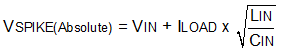
where
- VIN is the nominal supply voltage
- ILOAD is the load current
- LIN equals the effective inductance seen looking into the source
- CIN is the capacitance present at the input
Some of the applications may require the addition of a Transient Voltage Suppressor (TVS) to prevent transients from exceeding the absolute maximum ratings of the device. A typical circuit implementation with optional protection components (a ceramic capacitor, TVS and Schottky diode) is shown in Figure 9-20.
 Figure 9-20 Typical Circuit Implementation
With Optional Protection Components
Figure 9-20 Typical Circuit Implementation
With Optional Protection Components