JAJSCT5A March 2016 – May 2016 TPS3890
PRODUCTION DATA.
- 1 特長
- 2 アプリケーション
- 3 概要
- 4 改訂履歴
- 5 Device Comparison Table
- 6 Pin Configuration and Functions
- 7 Specifications
- 8 Detailed Description
- 9 Application and Implementation
- 10Power Supply Recommendations
- 11Layout
- 12デバイスおよびドキュメントのサポート
- 13メカニカル、パッケージ、および注文情報
9 Application and Implementation
NOTE
Information in the following applications sections is not part of the TI component specification, and TI does not warrant its accuracy or completeness. TI’s customers are responsible for determining suitability of components for their purposes. Customers should validate and test their design implementation to confirm system functionality.
9.1 Application Information
The following sections describe in detail how to properly use this device, depending on the requirements of the final application.
9.2 Typical Application
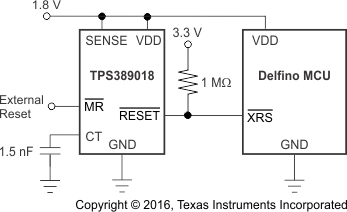
A typical application for the TPS389018 is shown in Figure 25. The TPS389018 can be used to monitor the 1.8-V VDD rail required by the TI Delfino™ microprocessor family. The open-drain RESET output of the TPS389018 is connected to the XRS input of the microprocessor. A reset event is initiated when the VDD voltage is less than VITN or when MR is driven low by an external source.
 Figure 25. TPS3890 Monitoring the Supply Voltage for a Delfino Microprocessor
9.2.1 Design Requirements
The TPS3890 RESET output can be used to drive the reset (XRS) input of a microprocessor. The RESET pin of the TPS3890 is pulled high with a 1-MΩ resistor; the reset delay time is controlled by the CT capacitor and is set depending on the reset requirement times of the microprocessor. During power-up, XRS must remain low for at least 1 ms after VDD reaches 1.5 V for the C2000™ Delfino family of microprocessors. For 100-MHz operation, the Delfino TMS320F2833x microcontroller uses a supply voltage of 1.8 V that must be monitored by the TPS3890.
9.2.2 Detailed Design Procedure
The primary constraint for this application is choosing the correct device to monitor the supply voltage of the microprocessor. The TPS389018 has a negative threshold of 1.73 V and a positive threshold of 1.74 V, making the device suitable for monitoring a 1.8-V rail. The secondary constraint for this application is the reset delay time that must be at least 1 ms to allow the Delfino microprocessor enough time to startup up correctly. Because a minimum time is required, the worst-case scenario is a supervisor with a high CT charging current (ICT) and a low CT comparator threshold (VCT). For applications with ambient temperatures ranging from –40°C to +125°C, CCT can be calculated using ICT(Max), VCT(MIN), and solving for CCT in Equation 1 such that the minimum capacitance required at the CT pin is 1.149 nF. If standard capacitors with ±20% tolerances are used, then the CT capacitor must be 1.5 nF or larger to ensure that the 1-ms delay time is met.
A 0.1-µF decoupling capacitor is connected to the VDD pin as a good analog design practice and a 1-MΩ resistor is used as the RESET pullup resistor to minimize the current consumption when RESET is asserted. The MR pin can be connected to an external signal if desired or connected to VDD if not used.
9.2.3 Application Curve
