SLUSBV0A May 2014 – JULY 2014 TPS40428
PRODUCTION DATA.
- 1 Features
- 2 Applications
- 3 Description
- 4 Revision History
- 5 Pin Configuration and Functions
- 6 Specifications
-
7 Detailed Description
- 7.1 Overview
- 7.2 Functional Block Diagram
- 7.3
Feature Description
- 7.3.1 Asynchronous Pulse Injection (API)
- 7.3.2 Adaptive Voltage Scaling (AVS)
- 7.3.3 Switching Frequency and Synchronization
- 7.3.4 Voltage Reference
- 7.3.5 Output Voltage and Remote Sensing Amplifier
- 7.3.6 Current Sensing and Temperature Sensing Modes
- 7.3.7 Current Sensing
- 7.3.8 Temperature Sensing
- 7.3.9 Current Sharing
- 7.3.10 Linear Regulators
- 7.3.11 Power Sequence Between TPS40428 Device and Power Stage
- 7.3.12 PWM Signal
- 7.3.13 Startup and Shutdown
- 7.3.14 Pre-Biased Output Start-up
- 7.3.15 PGOOD Indication
- 7.3.16 Overcurrent Protection
- 7.3.17 Output Overvoltage/Undervoltage Protection
- 7.3.18 Overtemperature Fault Protection
- 7.3.19 Input Undervoltage Lockout (UVLO)
- 7.3.20 Fault Communication
- 7.3.21 Fault Protection Summary
- 7.4 Device Functional Modes
- 7.5 Programming
- 7.6
Register Maps
- 7.6.1 PMBus General Description
- 7.6.2
PMBus Functionality
- 7.6.2.1 PMBus Address
- 7.6.2.2 PMBus Connections
- 7.6.2.3 PMBus Data Format
- 7.6.2.4 PMBus Output Voltage Adjustment
- 7.6.2.5 Reading the Output Current
- 7.6.2.6 Soft-Start Time
- 7.6.2.7 Turn-On/Turn-Off Delay and Sequencing
- 7.6.2.8
Supported PMBus Commands
- 7.6.2.8.1 PAGE (00h)
- 7.6.2.8.2 OPERATION (01h)
- 7.6.2.8.3 ON_OFF_CONFIG (02h)
- 7.6.2.8.4 CLEAR_FAULTS (03h)
- 7.6.2.8.5 WRITE_PROTECT (10h)
- 7.6.2.8.6 STORE_USER_ALL (15h)
- 7.6.2.8.7 RESTORE_USER_ALL (16h)
- 7.6.2.8.8 CAPABILITY (19h)
- 7.6.2.8.9 VOUT_MODE (20h)
- 7.6.2.8.10 VIN_ON (35h)
- 7.6.2.8.11 VIN_OFF (36h)
- 7.6.2.8.12 IOUT_CAL_GAIN (38h)
- 7.6.2.8.13 IOUT_CAL_OFFSET (39h)
- 7.6.2.8.14 IOUT_OC_FAULT_LIMIT (46h)
- 7.6.2.8.15 IOUT_OC_FAULT_RESPONSE (47h)
- 7.6.2.8.16 IOUT_OC_WARN_LIMIT (4Ah)
- 7.6.2.8.17 OT_FAULT_LIMIT (4Fh)
- 7.6.2.8.18 OT_WARN_LIMIT (51h)
- 7.6.2.8.19 TON_RISE (61h)
- 7.6.2.8.20 STATUS_BYTE (78h)
- 7.6.2.8.21 STATUS_WORD (79h)
- 7.6.2.8.22 STATUS_VOUT (7Ah)
- 7.6.2.8.23 STATUS_IOUT (7Bh)
- 7.6.2.8.24 STATUS_TEMPERATURE (7Dh)
- 7.6.2.8.25 STATUS_CML (7Eh)
- 7.6.2.8.26 STATUS_MFR_SPECIFIC (80h)
- 7.6.2.8.27 READ_VOUT (8Bh)
- 7.6.2.8.28 READ_IOUT (8Ch)
- 7.6.2.8.29 READ_TEMPERATURE_2 (8Eh)
- 7.6.2.8.30 PMBus_REVISION (98h)
- 7.6.2.8.31 MFR_SPECIFIC_00 (D0h)
- 7.6.2.8.32 MFR_SPECIFIC_04 (VREF_TRIM) (D4h)
- 7.6.2.8.33 MFR_SPECIFIC_05 (STEP_VREF_MARGIN_HIGH) (D5h)
- 7.6.2.8.34 MFR_SPECIFIC_06 (STEP_VREF_MARGIN_LOW) (D6h)
- 7.6.2.8.35 MFR_SPECIFIC_07 (PCT_VOUT_FAULT_PG_LIMIT) (D7h)
- 7.6.2.8.36 MFR_SPECIFIC_08 (SEQUENCE_TON_TOFF_DELAY) (D8h)
- 7.6.2.8.37 (E0h) MFR_SPECIFIC_16 (COMM_EEPROM_SPARE)
- 7.6.2.8.38 MFR_SPECIFIC_21 (OPTIONS) (E5h)
- 7.6.2.8.39 MFR_SPECIFIC_22 (PWM_OSC_SELECT) (E6h)
- 7.6.2.8.40 MFR_SPECIFIC_23 (MASK SMBALERT) (E7h)
- 7.6.2.8.41 MFR_SPECIFIC_25 (AVS_CONFIG) (E9h)
- 7.6.2.8.42 MFR_SPECIFIC_26 (AVS_ADDRESS) (EAh)
- 7.6.2.8.43 MFR_SPECIFIC_27 (AVS_DAC_DEFAULT) (EBh)
- 7.6.2.8.44 MFR_SPECIFIC_28 (AVS_CLAMP_HI) (ECh)
- 7.6.2.8.45 MFR_SPECIFIC_29 (AVS_CLAMP_LO) (EDh)
- 7.6.2.8.46 MFR_SPECIFIC_30 (TEMP_OFFSET) (EEh)
- 7.6.2.8.47 MFR_SPECIFIC_32 (API_OPTIONS) (F0h)
- 7.6.2.8.48 MFR_SPECIFIC_44 (DEVICE_CODE) (FCh)
-
8 Applications and Implementation
- 8.1 Application Information
- 8.2
Typical Application
- 8.2.1 Design Requirements
- 8.2.2
Detailed Design Procedure
- 8.2.2.1 Switching Frequency Selection
- 8.2.2.2 Inductor Selection
- 8.2.2.3 Output Capacitor Selection
- 8.2.2.4 Input Capacitor Selection
- 8.2.2.5 VDD, BP5, BP3 Bypass Capacitor
- 8.2.2.6 R-C Snubber
- 8.2.2.7 Current and Temperature Sensor
- 8.2.2.8 Power Sequence Between the TPS40428 Device and Power Stage
- 8.2.2.9 Output Voltage Setting and Frequency Compensation Selection
- 8.2.2.10 Key PMBus Parameter Selection
- 8.2.3 Application Curves
- 9 Power Supply Recommendations
- 10Layout
- 11Device and Documentation Support
- 12Mechanical, Packaging, and Orderable Information
パッケージ・オプション
メカニカル・データ(パッケージ|ピン)
- RHA|40
サーマルパッド・メカニカル・データ
- RHA|40
発注情報
1 Features
- Smart Power Mode in Factory Default (Compatible with TI Smart Power Stage CSD95378B and Pin-for-Pin Equivalent to TPS40425 – Non-Smart Power Mode in Factory Default)
- Single Supply Operation: 4.5 V to 20 V
- VOUT from 0.6 V
- Dual or Multi-Phase Synchronous Buck Controller
- Individual High-Speed AVS Interface
- Fast Transient Response
- Stackable up to Four Phases
- 2-, 3-, or 4-Phase Interleaved Phase Shifts
- Accurate Current Sharing
- PMBus Interface Capability
- Margining Up/Down with 2-mV Step
- Programmable Fault Limit and Response
- ±0.8% VOUT
- Accuracy Current Monitoring
- ±3°C External Temperature Monitoring In Smart Power Mode
- Programmable UVLO ON/OFF Thresholds
- Programmable Soft-Start Time, Turn-On Delay, and Turn-Off Delay
- On-Chip Non-Volatile Memory (NVM) to Store Custom Configurations
- 0.6-V Reference Voltage with 0.5% Accuracy from –40°C to 125°C
- Programmable ƒSW from 200 kHz to 1.5 MHz
- Supports Pre-biased Output
- Differential Remote Sensing
- Synchronization to an Extermal Clock
- OC/OV/UV/OT Fault Protection
- 40-Pin, 6 mm × 6 mm, QFN Package
2 Applications
- Wireless Infrastructure
- Switcher/Router Networking/Server/Storage
3 Description
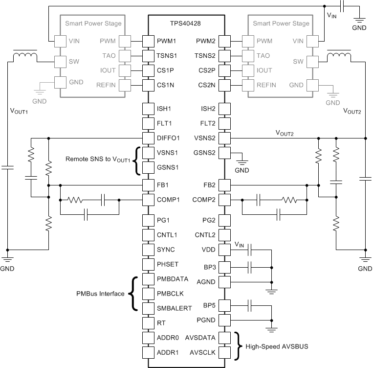
The TPS40428 device is a PMBus, synchronous buck, driverless controller. It operates in smart power mode with factory default settings, and it can operate in non-smart power mode after PMBus programing and power reboot. It can be configured for dual-output or 2-phase operation. It is also stackable up to 4 phases to support load current as high as 120 A. Interleaved phase shift for 2-. 3-, or 4-phases reduce the input and output ripples therefore reducing input and output capacitance.
The wide input voltage range can support 5-V and 12-V intermediate supply buses. The 0.5% reference voltage satisfies the need of precision voltage to the modern ASICs.
Using the PMBus standard, the TPS40428 device can program reference voltage, fault limit, UVLO threshold, soft-start time and turn-on and turn-off delay.
In addition, the device implements an accurate measurement system to monitor the output voltages, currents and temperatures for individual channels.
Device Information(1)
| PART NUMBER | PACKAGE | BODY SIZE (NOM) |
|---|---|---|
| TPS40428 | RHA (40) | 6.00 mm × 6.00 mm |
- For all available packages, see the orderable addendum at the end of the data sheet.
Simplified Application (Dual Output)