SLUSBV0A May 2014 – JULY 2014 TPS40428
PRODUCTION DATA.
- 1 Features
- 2 Applications
- 3 Description
- 4 Revision History
- 5 Pin Configuration and Functions
- 6 Specifications
-
7 Detailed Description
- 7.1 Overview
- 7.2 Functional Block Diagram
- 7.3
Feature Description
- 7.3.1 Asynchronous Pulse Injection (API)
- 7.3.2 Adaptive Voltage Scaling (AVS)
- 7.3.3 Switching Frequency and Synchronization
- 7.3.4 Voltage Reference
- 7.3.5 Output Voltage and Remote Sensing Amplifier
- 7.3.6 Current Sensing and Temperature Sensing Modes
- 7.3.7 Current Sensing
- 7.3.8 Temperature Sensing
- 7.3.9 Current Sharing
- 7.3.10 Linear Regulators
- 7.3.11 Power Sequence Between TPS40428 Device and Power Stage
- 7.3.12 PWM Signal
- 7.3.13 Startup and Shutdown
- 7.3.14 Pre-Biased Output Start-up
- 7.3.15 PGOOD Indication
- 7.3.16 Overcurrent Protection
- 7.3.17 Output Overvoltage/Undervoltage Protection
- 7.3.18 Overtemperature Fault Protection
- 7.3.19 Input Undervoltage Lockout (UVLO)
- 7.3.20 Fault Communication
- 7.3.21 Fault Protection Summary
- 7.4 Device Functional Modes
- 7.5 Programming
- 7.6
Register Maps
- 7.6.1 PMBus General Description
- 7.6.2
PMBus Functionality
- 7.6.2.1 PMBus Address
- 7.6.2.2 PMBus Connections
- 7.6.2.3 PMBus Data Format
- 7.6.2.4 PMBus Output Voltage Adjustment
- 7.6.2.5 Reading the Output Current
- 7.6.2.6 Soft-Start Time
- 7.6.2.7 Turn-On/Turn-Off Delay and Sequencing
- 7.6.2.8
Supported PMBus Commands
- 7.6.2.8.1 PAGE (00h)
- 7.6.2.8.2 OPERATION (01h)
- 7.6.2.8.3 ON_OFF_CONFIG (02h)
- 7.6.2.8.4 CLEAR_FAULTS (03h)
- 7.6.2.8.5 WRITE_PROTECT (10h)
- 7.6.2.8.6 STORE_USER_ALL (15h)
- 7.6.2.8.7 RESTORE_USER_ALL (16h)
- 7.6.2.8.8 CAPABILITY (19h)
- 7.6.2.8.9 VOUT_MODE (20h)
- 7.6.2.8.10 VIN_ON (35h)
- 7.6.2.8.11 VIN_OFF (36h)
- 7.6.2.8.12 IOUT_CAL_GAIN (38h)
- 7.6.2.8.13 IOUT_CAL_OFFSET (39h)
- 7.6.2.8.14 IOUT_OC_FAULT_LIMIT (46h)
- 7.6.2.8.15 IOUT_OC_FAULT_RESPONSE (47h)
- 7.6.2.8.16 IOUT_OC_WARN_LIMIT (4Ah)
- 7.6.2.8.17 OT_FAULT_LIMIT (4Fh)
- 7.6.2.8.18 OT_WARN_LIMIT (51h)
- 7.6.2.8.19 TON_RISE (61h)
- 7.6.2.8.20 STATUS_BYTE (78h)
- 7.6.2.8.21 STATUS_WORD (79h)
- 7.6.2.8.22 STATUS_VOUT (7Ah)
- 7.6.2.8.23 STATUS_IOUT (7Bh)
- 7.6.2.8.24 STATUS_TEMPERATURE (7Dh)
- 7.6.2.8.25 STATUS_CML (7Eh)
- 7.6.2.8.26 STATUS_MFR_SPECIFIC (80h)
- 7.6.2.8.27 READ_VOUT (8Bh)
- 7.6.2.8.28 READ_IOUT (8Ch)
- 7.6.2.8.29 READ_TEMPERATURE_2 (8Eh)
- 7.6.2.8.30 PMBus_REVISION (98h)
- 7.6.2.8.31 MFR_SPECIFIC_00 (D0h)
- 7.6.2.8.32 MFR_SPECIFIC_04 (VREF_TRIM) (D4h)
- 7.6.2.8.33 MFR_SPECIFIC_05 (STEP_VREF_MARGIN_HIGH) (D5h)
- 7.6.2.8.34 MFR_SPECIFIC_06 (STEP_VREF_MARGIN_LOW) (D6h)
- 7.6.2.8.35 MFR_SPECIFIC_07 (PCT_VOUT_FAULT_PG_LIMIT) (D7h)
- 7.6.2.8.36 MFR_SPECIFIC_08 (SEQUENCE_TON_TOFF_DELAY) (D8h)
- 7.6.2.8.37 (E0h) MFR_SPECIFIC_16 (COMM_EEPROM_SPARE)
- 7.6.2.8.38 MFR_SPECIFIC_21 (OPTIONS) (E5h)
- 7.6.2.8.39 MFR_SPECIFIC_22 (PWM_OSC_SELECT) (E6h)
- 7.6.2.8.40 MFR_SPECIFIC_23 (MASK SMBALERT) (E7h)
- 7.6.2.8.41 MFR_SPECIFIC_25 (AVS_CONFIG) (E9h)
- 7.6.2.8.42 MFR_SPECIFIC_26 (AVS_ADDRESS) (EAh)
- 7.6.2.8.43 MFR_SPECIFIC_27 (AVS_DAC_DEFAULT) (EBh)
- 7.6.2.8.44 MFR_SPECIFIC_28 (AVS_CLAMP_HI) (ECh)
- 7.6.2.8.45 MFR_SPECIFIC_29 (AVS_CLAMP_LO) (EDh)
- 7.6.2.8.46 MFR_SPECIFIC_30 (TEMP_OFFSET) (EEh)
- 7.6.2.8.47 MFR_SPECIFIC_32 (API_OPTIONS) (F0h)
- 7.6.2.8.48 MFR_SPECIFIC_44 (DEVICE_CODE) (FCh)
-
8 Applications and Implementation
- 8.1 Application Information
- 8.2
Typical Application
- 8.2.1 Design Requirements
- 8.2.2
Detailed Design Procedure
- 8.2.2.1 Switching Frequency Selection
- 8.2.2.2 Inductor Selection
- 8.2.2.3 Output Capacitor Selection
- 8.2.2.4 Input Capacitor Selection
- 8.2.2.5 VDD, BP5, BP3 Bypass Capacitor
- 8.2.2.6 R-C Snubber
- 8.2.2.7 Current and Temperature Sensor
- 8.2.2.8 Power Sequence Between the TPS40428 Device and Power Stage
- 8.2.2.9 Output Voltage Setting and Frequency Compensation Selection
- 8.2.2.10 Key PMBus Parameter Selection
- 8.2.3 Application Curves
- 9 Power Supply Recommendations
- 10Layout
- 11Device and Documentation Support
- 12Mechanical, Packaging, and Orderable Information
パッケージ・オプション
メカニカル・データ(パッケージ|ピン)
- RHA|40
サーマルパッド・メカニカル・データ
- RHA|40
発注情報
5 Pin Configuration and Functions
RHA PACKAGE
40 PINS
(TOP VIEW)
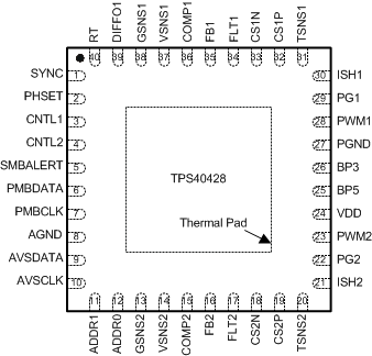
Pin Functions
| PIN | I/O | DESCRIPTION | |
|---|---|---|---|
| NAME | NO. | ||
| ADDR1 | 11 | I | High order address pin for PMBus device. Connect a resistor to AGND (see Table 3). |
| ADDR0 | 12 | I | Low order address pin for PMBus device. Connect a resistor to AGND (see Table 3). |
| AGND | 8 | — | Analog ground pin, used for analog signal. Connect to thermal pad directly. |
| AVSCLK | 10 | I | AVS clock |
| AVSDATA | 9 | I | AVS data |
| BP3 | 26 | O | 3.3-V bias power for logic. A low-ESR ceramic capacitor with a value of 0.33 µF or greater should be connected closely from this pin or to AGND. The maximum suggested capacitor value is 10 µF. |
| BP5 | 25 | O | Output bypass for the internal regulator. A low-ESR ceramic capacitor of 1 µF or greater should be connected closely from this pin to PGND pin. The maximum suggested capacitor value is 10 µF. |
| CNTL1 | 3 | I | Logic level input which starts or stops channel 1. An internal 6-µA current source pulls VCNTL1 up to VBP5 when the pin is floating. |
| CNTL2 | 4 | I | Logic level input which starts or stops channel 2. An internal 6-µA current source pulls VCNTL2 up to VBP5 when the pin is floating. |
| COMP1 | 36 | O | Output of the error amplifier 1 and connection node for loop feedback components |
| COMP2 | 15 | O | Output of the error amplifier 2 and connection node for loop feedback components |
| CS1N | 33 | I | Negative pin of current sense amplifier for channel 1. An internal, 4-kΩ resistor pulls CS1N to 1.24 V during smart power mode operation to provide a bias voltage required by smart power stage. |
| CS1P | 32 | I | Positive pin of current sense amplifier for channel 1 |
| CS2N | 18 | I | Negative pin of current sense amplifier for channel 2. An internal, 4-kΩ resistor pulls CS2N to 1.24 V during smart power mode operation to provide a bias voltage required by smart power stage. |
| CS2P | 19 | I | Positive pin of current sense amplifier for channel 2 |
| DIFFO1 | 39 | O | Remote Sense Amplifier Output for channel 1 |
| FB1 | 35 | I | Inverting input to the error amplifier 1. In normal operation, the voltage on this pin is equal to the internal reference voltage. Connect the FB1 pin to the BP5 pin to set the channel as slave channel. |
| FB2 | 16 | I | Inverting input to the error amplifier 2. In normal operation, the voltage on this pin is equal to the internal reference voltage. Connect the FB2 pin to the BP5 pin to set the channel as slave channel. |
| FLT1 | 34 | I/O | Fault signal of channel 1. An internal 100-kΩ resistor pulls FLT1 to BP3. |
| FLT2 | 17 | I/O | Fault signal of channel 2. An internal 100-kΩ resistor pulls FLT2 to BP3. |
| GSNS1 | 38 | I | Negative pin of Voltage Sense Signal for channel 1 |
| GSNS2 | 13 | I | Negative pin of Voltage Sense Signal for channel 2 |
| ISH1 | 30 | I | Current sharing signal of channel 1 for multi-phase mode |
| ISH2 | 21 | I | Current sharing signal of channel 2 for multi-phase mode |
| PG1 | 29 | O | Open drain power good indicator for channel 1 output voltage. This pin is pulled to ground internally in slave channel. |
| PG2 | 22 | O | Open drain power good indicator for channel 2 output voltage. This pin is pulled to ground internally in slave channel. |
| PGND | 27 | — | Power GND, used for BP5 bypass capacitor. Connect to thermal pad directly. |
| PHSET | 2 | I/O | Phase set for multiphase mode |
| PMBCLK | 7 | I | PMBus clock pin |
| PMBDATA | 6 | I/O | PMBus data pin |
| PWM1 | 28 | O | PWM signal for channel 1 |
| PWM2 | 23 | O | PWM signal for channel 2 |
| RT | 40 | I | Connecting a resistor from this pin to AGND sets the oscillator frequency |
| SMBALERT | 5 | O | PMBus alert pin. |
| SYNC | 1 | I/O | This is the synchronization pin for use with the external clock. The frequency of external SYNC signal must be 4 times of desired switching frequency during 1-, 2-, or 4- phases, and must be 3 times the desired switching frequency during 3-phase configuration. |
| TSNS1 | 31 | I | External temperature sense signal input for channel 1 |
| TSNS2 | 20 | I | External temperature sense signal input for channel 2 |
| VDD | 24 | I | Power input to the controller. A low-ESR ceramic capacitor with a value of 1-μF or greater should be connected closely from this pin to AGND. |
| VSNS1 | 37 | I | Positive pin of voltage sense signal for channel 1 |
| VSNS2 | 14 | I | Positive pin of voltage sense signal for channel 2 |