SLUSBV0A May 2014 – JULY 2014 TPS40428
PRODUCTION DATA.
- 1 Features
- 2 Applications
- 3 Description
- 4 Revision History
- 5 Pin Configuration and Functions
- 6 Specifications
-
7 Detailed Description
- 7.1 Overview
- 7.2 Functional Block Diagram
- 7.3
Feature Description
- 7.3.1 Asynchronous Pulse Injection (API)
- 7.3.2 Adaptive Voltage Scaling (AVS)
- 7.3.3 Switching Frequency and Synchronization
- 7.3.4 Voltage Reference
- 7.3.5 Output Voltage and Remote Sensing Amplifier
- 7.3.6 Current Sensing and Temperature Sensing Modes
- 7.3.7 Current Sensing
- 7.3.8 Temperature Sensing
- 7.3.9 Current Sharing
- 7.3.10 Linear Regulators
- 7.3.11 Power Sequence Between TPS40428 Device and Power Stage
- 7.3.12 PWM Signal
- 7.3.13 Startup and Shutdown
- 7.3.14 Pre-Biased Output Start-up
- 7.3.15 PGOOD Indication
- 7.3.16 Overcurrent Protection
- 7.3.17 Output Overvoltage/Undervoltage Protection
- 7.3.18 Overtemperature Fault Protection
- 7.3.19 Input Undervoltage Lockout (UVLO)
- 7.3.20 Fault Communication
- 7.3.21 Fault Protection Summary
- 7.4 Device Functional Modes
- 7.5 Programming
- 7.6
Register Maps
- 7.6.1 PMBus General Description
- 7.6.2
PMBus Functionality
- 7.6.2.1 PMBus Address
- 7.6.2.2 PMBus Connections
- 7.6.2.3 PMBus Data Format
- 7.6.2.4 PMBus Output Voltage Adjustment
- 7.6.2.5 Reading the Output Current
- 7.6.2.6 Soft-Start Time
- 7.6.2.7 Turn-On/Turn-Off Delay and Sequencing
- 7.6.2.8
Supported PMBus Commands
- 7.6.2.8.1 PAGE (00h)
- 7.6.2.8.2 OPERATION (01h)
- 7.6.2.8.3 ON_OFF_CONFIG (02h)
- 7.6.2.8.4 CLEAR_FAULTS (03h)
- 7.6.2.8.5 WRITE_PROTECT (10h)
- 7.6.2.8.6 STORE_USER_ALL (15h)
- 7.6.2.8.7 RESTORE_USER_ALL (16h)
- 7.6.2.8.8 CAPABILITY (19h)
- 7.6.2.8.9 VOUT_MODE (20h)
- 7.6.2.8.10 VIN_ON (35h)
- 7.6.2.8.11 VIN_OFF (36h)
- 7.6.2.8.12 IOUT_CAL_GAIN (38h)
- 7.6.2.8.13 IOUT_CAL_OFFSET (39h)
- 7.6.2.8.14 IOUT_OC_FAULT_LIMIT (46h)
- 7.6.2.8.15 IOUT_OC_FAULT_RESPONSE (47h)
- 7.6.2.8.16 IOUT_OC_WARN_LIMIT (4Ah)
- 7.6.2.8.17 OT_FAULT_LIMIT (4Fh)
- 7.6.2.8.18 OT_WARN_LIMIT (51h)
- 7.6.2.8.19 TON_RISE (61h)
- 7.6.2.8.20 STATUS_BYTE (78h)
- 7.6.2.8.21 STATUS_WORD (79h)
- 7.6.2.8.22 STATUS_VOUT (7Ah)
- 7.6.2.8.23 STATUS_IOUT (7Bh)
- 7.6.2.8.24 STATUS_TEMPERATURE (7Dh)
- 7.6.2.8.25 STATUS_CML (7Eh)
- 7.6.2.8.26 STATUS_MFR_SPECIFIC (80h)
- 7.6.2.8.27 READ_VOUT (8Bh)
- 7.6.2.8.28 READ_IOUT (8Ch)
- 7.6.2.8.29 READ_TEMPERATURE_2 (8Eh)
- 7.6.2.8.30 PMBus_REVISION (98h)
- 7.6.2.8.31 MFR_SPECIFIC_00 (D0h)
- 7.6.2.8.32 MFR_SPECIFIC_04 (VREF_TRIM) (D4h)
- 7.6.2.8.33 MFR_SPECIFIC_05 (STEP_VREF_MARGIN_HIGH) (D5h)
- 7.6.2.8.34 MFR_SPECIFIC_06 (STEP_VREF_MARGIN_LOW) (D6h)
- 7.6.2.8.35 MFR_SPECIFIC_07 (PCT_VOUT_FAULT_PG_LIMIT) (D7h)
- 7.6.2.8.36 MFR_SPECIFIC_08 (SEQUENCE_TON_TOFF_DELAY) (D8h)
- 7.6.2.8.37 (E0h) MFR_SPECIFIC_16 (COMM_EEPROM_SPARE)
- 7.6.2.8.38 MFR_SPECIFIC_21 (OPTIONS) (E5h)
- 7.6.2.8.39 MFR_SPECIFIC_22 (PWM_OSC_SELECT) (E6h)
- 7.6.2.8.40 MFR_SPECIFIC_23 (MASK SMBALERT) (E7h)
- 7.6.2.8.41 MFR_SPECIFIC_25 (AVS_CONFIG) (E9h)
- 7.6.2.8.42 MFR_SPECIFIC_26 (AVS_ADDRESS) (EAh)
- 7.6.2.8.43 MFR_SPECIFIC_27 (AVS_DAC_DEFAULT) (EBh)
- 7.6.2.8.44 MFR_SPECIFIC_28 (AVS_CLAMP_HI) (ECh)
- 7.6.2.8.45 MFR_SPECIFIC_29 (AVS_CLAMP_LO) (EDh)
- 7.6.2.8.46 MFR_SPECIFIC_30 (TEMP_OFFSET) (EEh)
- 7.6.2.8.47 MFR_SPECIFIC_32 (API_OPTIONS) (F0h)
- 7.6.2.8.48 MFR_SPECIFIC_44 (DEVICE_CODE) (FCh)
-
8 Applications and Implementation
- 8.1 Application Information
- 8.2
Typical Application
- 8.2.1 Design Requirements
- 8.2.2
Detailed Design Procedure
- 8.2.2.1 Switching Frequency Selection
- 8.2.2.2 Inductor Selection
- 8.2.2.3 Output Capacitor Selection
- 8.2.2.4 Input Capacitor Selection
- 8.2.2.5 VDD, BP5, BP3 Bypass Capacitor
- 8.2.2.6 R-C Snubber
- 8.2.2.7 Current and Temperature Sensor
- 8.2.2.8 Power Sequence Between the TPS40428 Device and Power Stage
- 8.2.2.9 Output Voltage Setting and Frequency Compensation Selection
- 8.2.2.10 Key PMBus Parameter Selection
- 8.2.3 Application Curves
- 9 Power Supply Recommendations
- 10Layout
- 11Device and Documentation Support
- 12Mechanical, Packaging, and Orderable Information
パッケージ・オプション
メカニカル・データ(パッケージ|ピン)
- RHA|40
サーマルパッド・メカニカル・データ
- RHA|40
発注情報
8 Applications and Implementation
8.1 Application Information
The TPS40428 device is a driverless synchronous buck controller with PMBus. it can work with a power stage device to convert a higher DC input voltage to a lower DC output voltage. The device is at smart power mode in factory default, the below design sample shows the TPS40428 device design with TI smart power stage CSD95378B in a dual-output configuration. The output voltages of channel 1 and channel 2 are set to 1.2 V and 1.8 V, respectively.
This design procedure provides steps how to select key component values, and set the appropriate behavioral options using the PMBus functionality. The design procedure is applied to channel 1 only in this section. User can apply similar calculation for channel 2.
8.2 Typical Application
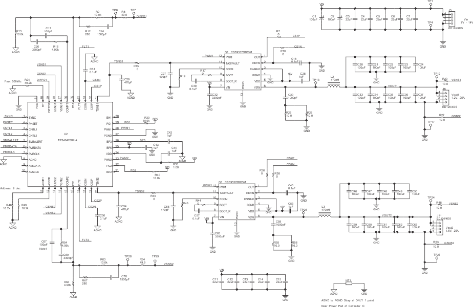 Figure 20. Typical Dual-Output Application Schematic
8.2.1 Design Requirements
This design example uses the input parameters summarized in Table 16.
Table 16. Design Example Specifications
| PARAMETER | TEST CONDITION | MIN | TYPE | MAX | UNIT | |
|---|---|---|---|---|---|---|
| VVIN | Input voltage | 7 | 12 | 14 | V | |
| VIN(ripple) | Input ripple voltage | IOUT = 25 A | 0.4 | V | ||
| VOUT | Output voltage | 1.2 | V | |||
| Line regulation | 7 V ≤ VVIN ≤ 14 V | 0.5% | ||||
| Load regulation | 0 V ≤ IOUT ≤ 25 A | 0.5% | ||||
| VP-P | Output ripple voltage | IOUT = 25 A | 10 | mV | ||
| ∆VOUT | Output voltage deviation during load transient | ∆IOUT = 10 A, VVIN = 12 V | 60 | mV | ||
| IOUT | Output current | 7 V ≤ VVIN ≤ 14 V | 0 | 25 | A | |
| tSS | Soft-start time | 2.7 | ms | |||
| IOC | Output peak current overcurrent trip point | 40 | A | |||
| η | Efficiency | IOUT = 25 A, VVIN = 12 V | 87% | |||
| fSW | Switching frequency | 500 | kHz | |||
8.2.2 Detailed Design Procedure
8.2.2.1 Switching Frequency Selection
Select a switching frequency for the regulator. There is a tradeoff between higher and lower switching frequencies for buck converters. Higher switching frequencies may produce smaller solution size using lower valued inductors and smaller output capacitors compared to a power supply that switches at a lower frequency. However, the higher switching frequency causes extra switching losses, which decrease efficiency and impact thermal performance. In this design, a moderate switching frequency of 500 kHz achieves both a small solution size and a high-efficiency operation. With the frequency selected, the timing resistor is calculated using Equation 10. The standard value 40.2 kΩ is used in the design.

8.2.2.2 Inductor Selection
Use Equation 11 to calculate the value of the output inductance. The coefficient KIND represents the amount of inductor ripple current relative to the maximum output current. The output capacitor filters the inductor ripple current. Therefore, choosing a high inductor ripple current impacts the selection of the output capacitor since the output capacitor must have a ripple current rating equal to or greater than the inductor ripple current. Generally, maintain the KIND coefficient between 0.2 and 0.3 for balanced performance. Using this target ripple current, Equation 11 describes the required inductor size calculation.

With a selected KIND of 0.25, the target inductance (L1) calcualtes to 351 nH. Considering the variation and de-rating of inductance, this application uses a 470-nH inductor (Wurth Electronics part number 744355147). Equation 12 calculates the inductor ripple current . Equation 13 calculates the RMS current. Equation 13 calculates the peak current. Use these values to select an inductor with the approximate target inductance value, and to select current ratings that allow normal operation with some margin.


The WE 744355147 inductor is rated for 30 A RMS current and 50 A saturation current. Using this inductor, the ripple current IRIPPLE = 4.7 A, the RMS inductor current IL(rms) = 25.04 A, and peak inductor current IL(peak) = 27.33 A.
8.2.2.3 Output Capacitor Selection
There are two primary considerations for selecting the value of the output capacitor.
- the output voltage deviation during load transient.
- the output voltage ripple
8.2.2.3.1 Output Voltage Deviation During Load Transient
The desired response to a load transient is the first criterion. The output capacitor must supply the load with the required current when not immediately provided by the regulator. When the output capacitor supplies load current, the impedance of the capacitor affects the magnitude of voltage deviation during the transient.
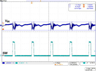
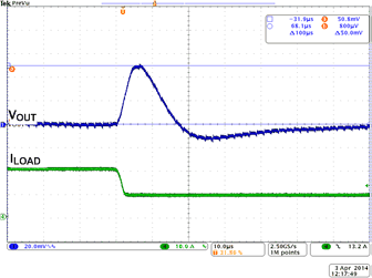
In order to meet the requirements for control loop stability, TPS40428 requires the addition of compensation components in the design of the error amplifier. While these compensation components provide for a stable control loop, they often also reduce the speed with which the regulator can respond to load transients. Figure 21 shows the waveforms of inductor current (IL) and voltage deviation (∆VOUT) during a ∆IOUT load step up. It also shows the response time (tRESP) that inductor current changes from previous load current to the new load current.
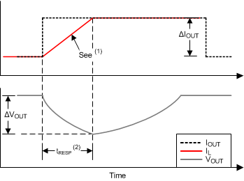
The response time tRESP can be calculated using Equation 15 and Equation 16. Usually the cross frequency fCO is set to between one tenth and one fifth of the switching frequency, fSW. In the design the switching frequency is 500 kHz, therefore 50 kHz is used for fCO in the calculation. Equation 18 calculates the minimum required output capacitance COUT(min).


8.2.2.3.2 Output Voltage Ripple
The output voltage ripple is the second criterion for selecting the value of the output capacitor. Equation 19 calculates the minimum output capacitance required to meet the output voltage ripple specification.

In this case, the target maximum output voltage ripple is 10 mV. Under this requirement, the minimum output capacitance for ripple is 116 µF. Because this capacitance value is smaller than the output capacitance required for the transient response, select the output capacitance value based on the transient requirement. Considering the variation and de-rating of capacitance, in this design, use ten 100-µF low-ESR ceramic capacitors to meet the transient specification with sufficient margin. Therefore COUT = 1000 µF.
Using the known target output capacitance value, Equation 20 calculates the maximum ESR the output capacitor bank allowed to meet the output voltage ripple specification. Equation 20 indicates the ESR should be less than 1.9 mΩ. Each 100-µF ceramic capacitor contributes approximately 2 mΩ, making the effective ESR of the output capacitor bank approximately 0.2 mΩ, meeting the specification with sufficient margin.

8.2.2.4 Input Capacitor Selection
The power stage input decoupling capacitance (effective capacitance at the VIN and PGND terminals) must be sufficient to supply the high switching currents demanded when the high-side MOSFET switches on, while providing minimal input voltage ripple as a result. This effective capacitance includes any DC bias effects. The voltage rating of the input capacitor must be greater than the maximum input voltage with derating. The capacitor must also have a ripple current rating greater than the maximum input current ripple to the device during full load. Use Equation 21 to estimate the input rms current.

The minimum input capacitance and ESR values for a given input voltage ripple specification, VIN(ripple), are shown in Equation 22 and Equation 23. The input ripple is composed of a capacitive portion, VRIPPLE(cap), and a resistive portion, VRIPPLE(esr).


The value of a ceramic capacitor varies significantly over temperature and the amount of DC bias applied to the capacitor. Minimize the capacitance variations due to temperature by selecting a dielectric material that is stable over temperature. X5R and X7R ceramic dielectrics are usually selected for power regulator capacitors because they have a high capacitance to volume ratio and are fairly stable over temperature.
The input capacitor must also be selected with the DC bias taken into account. This design requires a ceramic capacitor with at least a 25-V voltage rating to support the maximum input voltage. For this design, allow 0.1-V input ripple for VRIPPLE(cap), and 0.2-V input ripple for VRIPPLE(esr). Using Equation 22 and Equation 23, the minimum input capacitance for this design is 42.8 µF, and the maximum ESR is 7.3 mΩ. For this design example, five 22-μF, 25-V ceramic capacitors and two additional 100-μF, 25-V low-ESR electrolytic capacitors in parallel were selected for the power stage with sufficient margin.
A high frequency input voltage bypass capacitor is suggested to be placed close to the power stage to help with ringing reduction. Please refer to the datasheet of the power stage device for more application information of input capacitors.
8.2.2.5 VDD, BP5, BP3 Bypass Capacitor
The BP3 pin requires a minimum capacitance of 0.33 µF connected to AGND. The BP5 pin requires approximately 1 µF of capacitance connected to PGND. The VDD pin requires approximately 1 µF of capacitance connected to AGND. To filter ripple on VIN, a small value resistor is recommended to be placed between the VDD pin and the VIN pin.
In this design, a 1-µF capacitor is used for all VDD, BP5 and BP3 pins. All bypass capacitors must be placed close to the device. Place a 1-Ω resistor between the VDD pin and the VIN pin.
8.2.2.6 R-C Snubber
An R-C snubber needs to be placed between the switching node and PGND to reduce voltage spike on switching node. The power rating of the resistor needs to be larger than the power dissipation on the resistor with sufficient margin. To balance efficiency and spike level, a 1-nF capacitor and two 10-Ω resistors are chosen in the design. Please refer to the datasheet of the power stage device for more application information.
8.2.2.7 Current and Temperature Sensor
During smart-power mode operation, the TPS40428 device receives the current and temperature signals from the smart power stage. The CSxP and CSxN pins of the TPS40428 device are connected to the IOUT and REFIN pins respectively of the power stage, . Local bypass capacitors are required for CSxN pin and REFIN pin, the recommended value of bypass capacitors is 100 nF. This design suggests that no capacitor be placed between the CSxP and CSxN pins.
The TSNSx pin of the TPS40428 device is connected to TAO pin of power stage. Local bypass capacitors are recommended for both TSNSx pin and TAO pin. The recommended value for both bypass capacitors is 470 pF. To increase the immunity of the TAO pin signal-to-noise ratio, place a 121-kΩ resistor between the TAO pin and ground.
8.2.2.8 Power Sequence Between the TPS40428 Device and Power Stage
Before soft-start operation begins to generate a PWM signal, the VDD voltage for power stage must be prepared. Without preparation, the TPS40428 outputs the PWM signal at maximum duty cycle, because the power stage is not working and output voltage is not regulated.
The supply voltage (VDD) for the power stage must be above its threshold until the TPS40428 device is turned off.
8.2.2.9 Output Voltage Setting and Frequency Compensation Selection
A feedback divider between the DIFFO pin and AGND sets the output voltage. This design selects an R1 value of 10 kΩ. Using R1 and the desired output voltage, and calculate the value of the RBIAS resistor using Equation 24 to be 10 kΩ.

The TPS40428 device uses voltage mode control with input feedforward at single phase dual-output configuration. See the presentation Under the Hood of Low-Voltage DC/DC Converters from the 2003 TI Power Supply Design Seminar for an in-depth discussion of voltage-mode feedback and control. Click SLUP206 to download a copy. Frequency compensation can be accomplished using standard techniques. TI also provides a compensation calculator tool to streamline compensation design. In the TPS40k Loop Compensation Tool, the device parameters, cross frequency and phase margin are set as below.
The device parameters entered into the loop compenation tool for this design are:
- VVRAMP = VVIN/10
- VREF = 0.6 V
- GBWP = 50 MHz
- DC Gain = 80dB
- fCO = 50 kHz
- Phase Margin = 55°
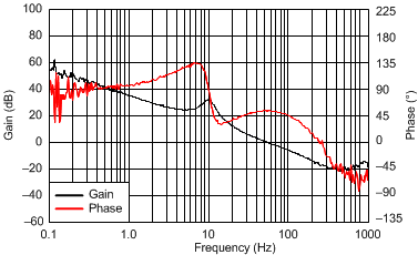
The tool provides the recommended compensation components, and approximate bode plots. As a starting point, the crossover frequency should be set to 1/10 fSW, and the phase margin at crossover should be greater than 45°. The resulting plots should be reviewed for a few common considerations. The error amplifier gain should not hit the error amplifier gain bandwidth product (GBWP), and the error amplifier gain at switching frequency region is recommended to be approximately 20dB in general. Use the tool to calculate the system bode plot at different loading conditions to ensure that the phase does not drop below zero prior to crossover, as this condition is known as conditional stability.
The design tool provides the compensation network values as a starting point. It is always recommended to measure the real system bode plot after the design and adjust the compensation values accordingly.
These compensation values are from the tool calculation and optimization based on the measured data.
- R1 = 10 kΩ
- R1 = 0.28 kΩ
- R3 = 5 kΩ
- RBIAS = 10 kΩ
- C1 = 1500 pF
- C2 = 3300 pF
- C3 = 100 pF
8.2.2.10 Key PMBus Parameter Selection
The following subsections summarize some of the key design parameters for the TPS40428 device can be configured via the PMBus interface, and stored to its non-volatile memory (NVM) for future use.
8.2.2.10.1 MFR_SPECIFIC_21 (OPTIONS)
The EN_SPS bit in MFR_SPECIFIC_21 register is set to 1b in factory default. It must be set to 1b to allow TPS40428 to work at smart power mode.
The default value 20 V/V is recommended for CH1_CSGAIN_SEL and CH2_CSGAIN_SEL bits for most applications.
The en_adc_ctl bit is set to 1b in factory default mode to enable ADC operation such that the output voltage, output current and temperature information can be provided by the TPS40428 device through the PMBus interface.
8.2.2.10.1.1 IOUT_CAL_GAIN
The default value 0.5035 mΩ must be used for accuracy current readout when the TPS40428 device is operating in smart power mode.
8.2.2.10.1.2 Enable and UVLO
The ON_OFF_CONFIG command is used to select the turn-on behavior of the converter. For this example, the CNTL pin was used to enable or disable the converter, regardless of the state of OPERATION, as long as input voltage is present, and above the UVLO threshold. The CNTL pin is pulled to BP5 via an internal 6 µA current source if it is floating.
8.2.2.10.1.3 Soft-Start Time
The TON_RISE command sets the soft-start time, the charging current for the output capacitors needs to be considered when selecting the soft-start time. In some applications (e.g., those with large amounts of output capacitance) this current can cause false tripping of the overcurrent protection circuitry if the soft-start time is not properly selected. To avoid false tripping, the output capacitor charging current should be included when choosing a soft-start time and overcurrent threshold. The capacitor charging current can be calculated using Equation 25.

8.2.2.10.1.4 Overcurrent Threshold and Response
The IOUT_OC_FAULT_LIMIT command sets the overcurrent threshold. The TPS40428 device uses inductor peak current value for overcurrent detecting. The current limit should be set to the maximum inductor peak current, plus the output capacitor charging current during start-up, plus some margin for load transients and component variation. The amount of margin required depends on the individual application, but a suggested point is between 30% and 50%. For this application, the maximum inductor peak current is 27.33 A, the output capacitor charging current is 0.44 A. This design allows some extra margin, so an overcurrent threshold of 40 A (peak current) was selected.
The IOUT_OC_FAULT_RESPONE command sets the desired response to an overcurrent event. In this example, the converter is configured to hiccup in the event of an overcurrent. TPS40428 device can also be configured to latch in the event of an overcurrent.
8.2.3 Application Curves
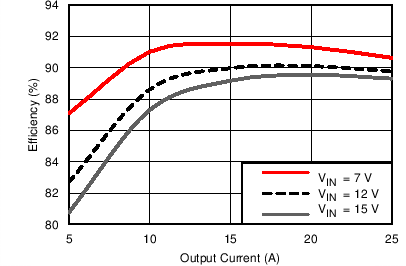 Figure 22. Effiency vs Output Current
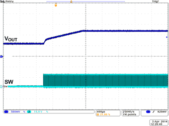
| VIN = 12 V | IOUT = 25 A |
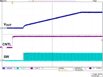
| VIN = 12 V | IOUT = 25 A |
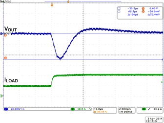
| VIN = 12 V | Div = 5A/µs |
| VIN = 12 V | IOUT = 0 A |
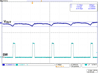
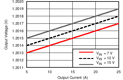 Figure 23. Load Regulation
| VIN = 12 V | IOUT = 25 A |
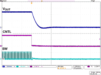
| VIN = 12 V | IOUT = 25 A |
| VIN = 12 V | Div = 5A/µs |
| VIN = 12 V | IOUT = 25 A | |