SLUSBV0A May 2014 – JULY 2014 TPS40428
PRODUCTION DATA.
- 1 Features
- 2 Applications
- 3 Description
- 4 Revision History
- 5 Pin Configuration and Functions
- 6 Specifications
-
7 Detailed Description
- 7.1 Overview
- 7.2 Functional Block Diagram
- 7.3
Feature Description
- 7.3.1 Asynchronous Pulse Injection (API)
- 7.3.2 Adaptive Voltage Scaling (AVS)
- 7.3.3 Switching Frequency and Synchronization
- 7.3.4 Voltage Reference
- 7.3.5 Output Voltage and Remote Sensing Amplifier
- 7.3.6 Current Sensing and Temperature Sensing Modes
- 7.3.7 Current Sensing
- 7.3.8 Temperature Sensing
- 7.3.9 Current Sharing
- 7.3.10 Linear Regulators
- 7.3.11 Power Sequence Between TPS40428 Device and Power Stage
- 7.3.12 PWM Signal
- 7.3.13 Startup and Shutdown
- 7.3.14 Pre-Biased Output Start-up
- 7.3.15 PGOOD Indication
- 7.3.16 Overcurrent Protection
- 7.3.17 Output Overvoltage/Undervoltage Protection
- 7.3.18 Overtemperature Fault Protection
- 7.3.19 Input Undervoltage Lockout (UVLO)
- 7.3.20 Fault Communication
- 7.3.21 Fault Protection Summary
- 7.4 Device Functional Modes
- 7.5 Programming
- 7.6
Register Maps
- 7.6.1 PMBus General Description
- 7.6.2
PMBus Functionality
- 7.6.2.1 PMBus Address
- 7.6.2.2 PMBus Connections
- 7.6.2.3 PMBus Data Format
- 7.6.2.4 PMBus Output Voltage Adjustment
- 7.6.2.5 Reading the Output Current
- 7.6.2.6 Soft-Start Time
- 7.6.2.7 Turn-On/Turn-Off Delay and Sequencing
- 7.6.2.8
Supported PMBus Commands
- 7.6.2.8.1 PAGE (00h)
- 7.6.2.8.2 OPERATION (01h)
- 7.6.2.8.3 ON_OFF_CONFIG (02h)
- 7.6.2.8.4 CLEAR_FAULTS (03h)
- 7.6.2.8.5 WRITE_PROTECT (10h)
- 7.6.2.8.6 STORE_USER_ALL (15h)
- 7.6.2.8.7 RESTORE_USER_ALL (16h)
- 7.6.2.8.8 CAPABILITY (19h)
- 7.6.2.8.9 VOUT_MODE (20h)
- 7.6.2.8.10 VIN_ON (35h)
- 7.6.2.8.11 VIN_OFF (36h)
- 7.6.2.8.12 IOUT_CAL_GAIN (38h)
- 7.6.2.8.13 IOUT_CAL_OFFSET (39h)
- 7.6.2.8.14 IOUT_OC_FAULT_LIMIT (46h)
- 7.6.2.8.15 IOUT_OC_FAULT_RESPONSE (47h)
- 7.6.2.8.16 IOUT_OC_WARN_LIMIT (4Ah)
- 7.6.2.8.17 OT_FAULT_LIMIT (4Fh)
- 7.6.2.8.18 OT_WARN_LIMIT (51h)
- 7.6.2.8.19 TON_RISE (61h)
- 7.6.2.8.20 STATUS_BYTE (78h)
- 7.6.2.8.21 STATUS_WORD (79h)
- 7.6.2.8.22 STATUS_VOUT (7Ah)
- 7.6.2.8.23 STATUS_IOUT (7Bh)
- 7.6.2.8.24 STATUS_TEMPERATURE (7Dh)
- 7.6.2.8.25 STATUS_CML (7Eh)
- 7.6.2.8.26 STATUS_MFR_SPECIFIC (80h)
- 7.6.2.8.27 READ_VOUT (8Bh)
- 7.6.2.8.28 READ_IOUT (8Ch)
- 7.6.2.8.29 READ_TEMPERATURE_2 (8Eh)
- 7.6.2.8.30 PMBus_REVISION (98h)
- 7.6.2.8.31 MFR_SPECIFIC_00 (D0h)
- 7.6.2.8.32 MFR_SPECIFIC_04 (VREF_TRIM) (D4h)
- 7.6.2.8.33 MFR_SPECIFIC_05 (STEP_VREF_MARGIN_HIGH) (D5h)
- 7.6.2.8.34 MFR_SPECIFIC_06 (STEP_VREF_MARGIN_LOW) (D6h)
- 7.6.2.8.35 MFR_SPECIFIC_07 (PCT_VOUT_FAULT_PG_LIMIT) (D7h)
- 7.6.2.8.36 MFR_SPECIFIC_08 (SEQUENCE_TON_TOFF_DELAY) (D8h)
- 7.6.2.8.37 (E0h) MFR_SPECIFIC_16 (COMM_EEPROM_SPARE)
- 7.6.2.8.38 MFR_SPECIFIC_21 (OPTIONS) (E5h)
- 7.6.2.8.39 MFR_SPECIFIC_22 (PWM_OSC_SELECT) (E6h)
- 7.6.2.8.40 MFR_SPECIFIC_23 (MASK SMBALERT) (E7h)
- 7.6.2.8.41 MFR_SPECIFIC_25 (AVS_CONFIG) (E9h)
- 7.6.2.8.42 MFR_SPECIFIC_26 (AVS_ADDRESS) (EAh)
- 7.6.2.8.43 MFR_SPECIFIC_27 (AVS_DAC_DEFAULT) (EBh)
- 7.6.2.8.44 MFR_SPECIFIC_28 (AVS_CLAMP_HI) (ECh)
- 7.6.2.8.45 MFR_SPECIFIC_29 (AVS_CLAMP_LO) (EDh)
- 7.6.2.8.46 MFR_SPECIFIC_30 (TEMP_OFFSET) (EEh)
- 7.6.2.8.47 MFR_SPECIFIC_32 (API_OPTIONS) (F0h)
- 7.6.2.8.48 MFR_SPECIFIC_44 (DEVICE_CODE) (FCh)
-
8 Applications and Implementation
- 8.1 Application Information
- 8.2
Typical Application
- 8.2.1 Design Requirements
- 8.2.2
Detailed Design Procedure
- 8.2.2.1 Switching Frequency Selection
- 8.2.2.2 Inductor Selection
- 8.2.2.3 Output Capacitor Selection
- 8.2.2.4 Input Capacitor Selection
- 8.2.2.5 VDD, BP5, BP3 Bypass Capacitor
- 8.2.2.6 R-C Snubber
- 8.2.2.7 Current and Temperature Sensor
- 8.2.2.8 Power Sequence Between the TPS40428 Device and Power Stage
- 8.2.2.9 Output Voltage Setting and Frequency Compensation Selection
- 8.2.2.10 Key PMBus Parameter Selection
- 8.2.3 Application Curves
- 9 Power Supply Recommendations
- 10Layout
- 11Device and Documentation Support
- 12Mechanical, Packaging, and Orderable Information
パッケージ・オプション
メカニカル・データ(パッケージ|ピン)
- RHA|40
サーマルパッド・メカニカル・データ
- RHA|40
発注情報
7 Detailed Description
7.1 Overview
The TPS40428 device is a PMBus synchronous buck driverless controller. It can be configured as a dual-output or single output two phase. It is also stackable up to 4 phases to support load current as high as 120 A. Interleaved phase shift for 2-, 3-, or 4-phase operation reduces the input and output ripples therefore reducing input and output capacitance.
When operating in dual-output mode, the device implements voltage mode control with input feed-forward architecture. With this architecture, the benefits are less noise sensitivity, no control instability issues for small DCR applications, and a smaller minimum controllable on-time, often desired for high conversion ratio applications. In multi-phase mode, the device implements a current-sharing loop to ensure a balance of current between phases.
The wide input voltage range supports 5-V and 12-V intermediate buses. The 0.5% reference voltage satisfies the need for precision voltage required by modern ASICs. PMBus functionality allows the TPS40428 device to program margining function, reference voltage, fault limit, UVLO threshold, soft-start time and turn-on delay time and turn-off delay time. In addition, an accurate measurement system monitors the output voltages, currents and temperatures for individual channels.
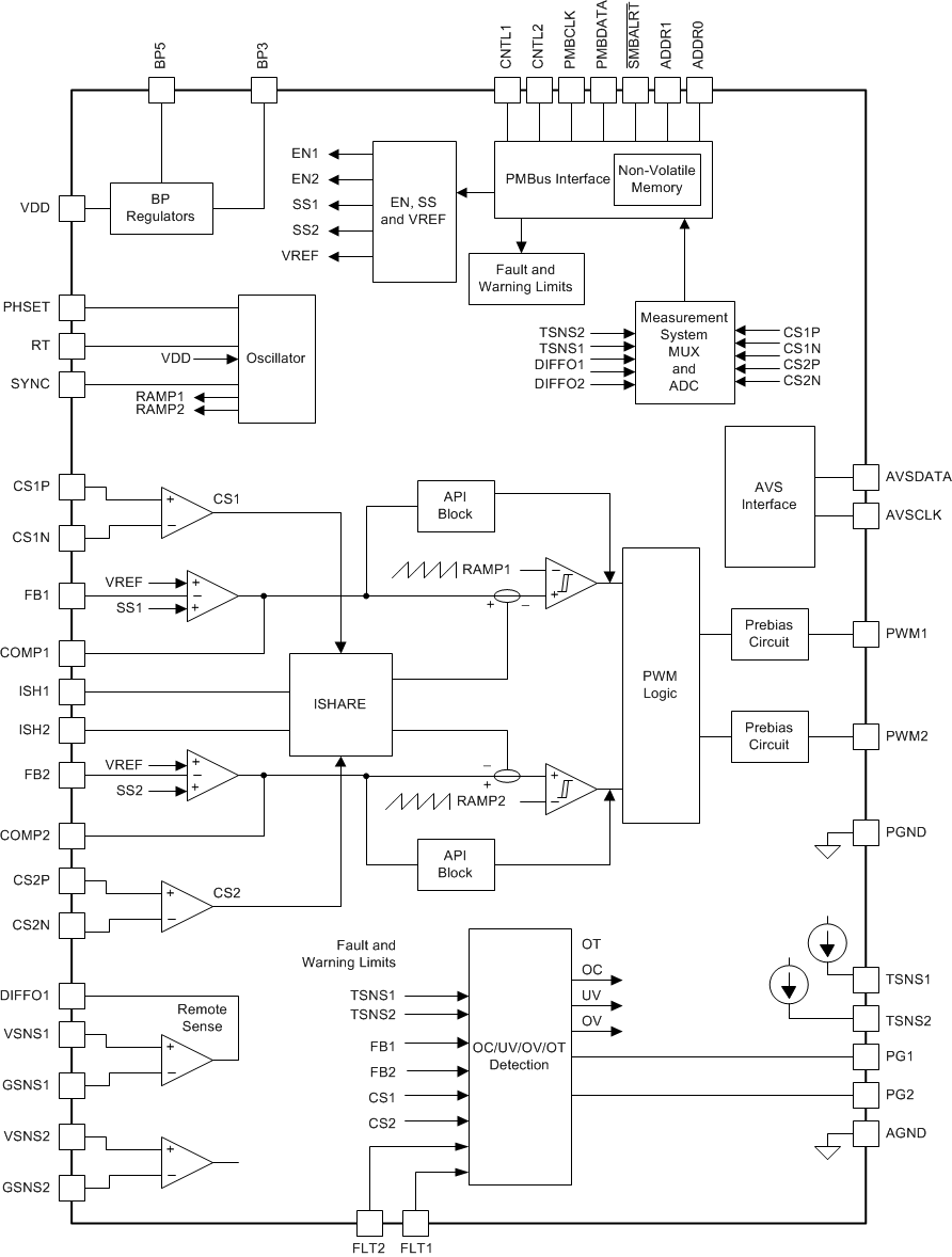
7.2 Functional Block Diagram
7.3 Feature Description
7.3.1 Asynchronous Pulse Injection (API)
The TPS40428 device implements a TI proprietary control scheme to achieve fast transient response. This scheme has the following key features:
- Voltage mode with API (asynchronous pulse injection) technology
- Fast transient response to reduce output capacitance
Figure 10 shows the control loop with API technology. The control scheme continuously senses the voltage on the COMP pin to determine a transient event that could require a sudden increase in duty-cycle. Upon detecting such an event, additional pulses are asynchronously injected in the PWM stream to quickly respond to the transient and arrest any undershoot in the output voltage.
During load step-up, the deviation of the COMP pin voltage must be above the API comparator threshold to trigger API. Refer to the MFR_SPECIFIC_32 (API_OPTIONS) (F0h) section for more information.
The API response can be delayed by compensation, parasitic impedance between the output inductor and the voltage sense point. If the delay is large, the asynchronous PWM might inject too much energy and result in overshoot during load step-up. In this case, it is imperative to optimize the compensation and reduce the parasitic impedance. If these efforts cannot reduce the overshoot to an acceptable level, disable the API function.
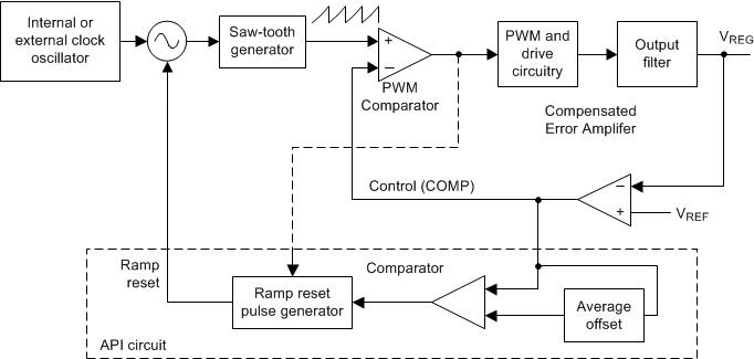 Figure 10. Asynchronous Pulse Injection (API) Block Diagram
7.3.2 Adaptive Voltage Scaling (AVS)
AVS provides output voltage scaling. AVSBus is a 2-wire communication link that enables bi-directional communication between one ASIC and one or more slave devices for controlling voltage scaling. The two wires required for communication are AVS_Clock and AVS_Data. The AVSBus interface could be used exclusively once PMBus has configured the device properly. The AVS commands can select channel 1 or channel 2 of slave device.
AVSBus is scalable for use with multiple slave devices, and allows for independent control of multiple rails within each slave. This scalability is achieved without sacrificing response time for simpler designs with a single slave, by means of configuration settings.
NOTE
PMBus commands are required to:
- configure the device to AVS mode
- set AVS address for the device
- set transition slew rate of output voltage
7.3.3 Switching Frequency and Synchronization
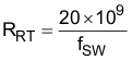
A resistor from the RT pin to AGNG sets the switching frequency (fSW). The RRT resistor value is calculated in Equation 1 for switching frequencies below 800 kHz. For switching frequencies above 800 kHz, refer to Table 1 for RRT resistor values.
where
- RRT is the resistor from the RT pin to AGND, in Ω
- ƒSW is the desired switching frequency, in Hz
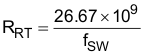
The switching frequency during 3-phase operation is 1.33 times of that at 1-, 2-, or 4-phase operation with the same RT resistor value. Use Equation 2 to calculate the RT resistor value for 3-phase operation.
where
- RRT is the resistor from the RT pin to AGND, in Ω
- ƒSW is the desired switching frequency, in Hz
Table 1. Setting the Switching Frequency
| TIMING RESISTANCE RRT (kΩ) |
SWITCHING FREQUENCY ƒSW (kHz) |
|---|---|
| 11 | 1520 |
| 11.8 | 1450 |
| 12.4 | 1400 |
| 13 | 1370 |
| 15 | 1208 |
| 20 | 948 |
| 24.9 | 776 |
The accuracy of the frequency setting is ±10%. For 3-phase and 4-phase applications, the RT resistors should be identical for both the controllers. In 3-phase and 4-phase applications, the device achieves clock and phase synchronization between the two controllers by connecting the SYNC pins and PHSET pins of the master controller to the corresponding pins on the slave controller. Phase configuration indicating number of phases is set according to the PMBus manufacturer specific command MFR_SPECIFIC_22 (E6h).
The switching frequency can be synchronized by an external clock on the SYNC pin. The frequency of the SYNC signal must be 4 times the switching frequency during 1-, 2-, or 4-phase operation, and must be 3 times the switching frequency during 3-phase operation. The SYNC signal must be a square waveform with 50% duty cycle. The high-level threshold must be above 2 V, and the low-level threshold must be below 0.8 V. The change on SYNC and PHSET setting occurs only after a power re-cycle.
7.3.4 Voltage Reference
The 600-mV bandgap cell is internally connected to the non-inverting input of the error amplifier. The reference voltage is 600 mV with ±0.5% between –40°C and 125°C.
7.3.5 Output Voltage and Remote Sensing Amplifier
Setting the output voltage is very similar to that of a traditional analog controller using a voltage divider from the output to the feedback (FB) pin. The output voltage must be divided to the nominal reference voltage of 600 mV. Figure 11 shows the typical connections for the controller. The voltage at the load is sensed using the unity gain differential voltage sense amplifier. This type of sensing provides better load regulation (see electrical specifications for the maximum output voltage of the differential sense amplifier).
To prevent output voltage out of regulation, ensure the maximum allowed DIFFO1 voltage (VBP5 – 0.2 V) is larger than actual output voltage at any time including when BP5 ramps down. For output voltages above the DIFFO1 pin specification, connect the output voltage directly to the junction of R1 and C1, leave DIFFO1 open and do not connect the VSNS1 pin to the output voltage. If the design includes a resistor divider before the remote sensing amplifier, the output voltage readout on PMBus is equal to the voltage between VSNS1 and GSNS1.
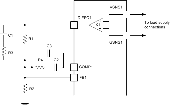 Figure 11. Setting the Output Voltage
where
- VFB is the feedback voltage
- VOUT is the desired output voltage
- R1 and R2 are in the same units
NOTE
There is no DIFFO2 pin. In dual-output mode, VSNS2 and GSNS2 are connected to the load for channel 2 and the DIFFO2 signal is used internally for voltage monitoring. Connect the output directly to the junction of R1 and C1 for channel 2 to set the output voltage and for feedback.
The feedback voltage can be changed –30% to 10% from the nominal 600 mV using PMBus commands. The output voltage can vary by the same percentage.
7.3.6 Current Sensing and Temperature Sensing Modes
The TPS40428 device can operate in two operating modes as far as the current and temperature sensing methods are concerned. The device operates at smart power mode in factory default setting, and it can also operate at non-smart power mode after PMBus programing and power reboot. Refer to the MFR_SPECIFIC_21 (OPTIONS) (E5h) section for more information.
Consider using the TPS40425 device if non smart-power mode in factory default is preferred in an application. Refer to the TPS40425 datasheet (SLUSBO6) for more information.
During smart power operation, an internal 4-kΩ resistor pulls the CSxN pin of the TPS40428 device to 1.24 V once VDD voltage is applied. When a board is configured to operate using non smart-power mode, but the TPS40428 device configured for smart power mode is used, the CSxN voltage charges the output capacitor to 1.24 V because the CSxN pin is connected to output for DCR sensing. This problem can avoid in two ways, either:
- the TPS40428 must be reprogrammed to non smart-power mode before it is assembled on the board, or
- the application must include a small-value (on the order of 100 Ω) resistor between output and ground such that a very small portion of the CSxN pin voltage is applied on output
7.3.6.1 Non Smart-Power Operation
Current sensing is based on inductor DCR (direct current resistance) sensing or a separate current sense resistor. Temperature sensing is based on the ΔVbe measurement of an external diode (x3904). This mode can be used with standard power-stages, such as the CSD95372A.
If inductor DCR is used for current sensing, the TPS40428 device compensates for the temperature variation of DCR value by using the temperature sensed at the external sensor for that channel. The temperature-compensated DCR value is used both for reporting inductor current over PMBus and for overcurrent fault and warning functions.
If a sense resistor is used for current sensing and the temperature variation of resistor value is very small, the temperature compensation in the TPS40428 device can be disabled.
7.3.6.2 Smart-Power Operation.
The current sensing function in the TPS40428 device is based on sensed voltage reported by the smart power-stage (at 5 mV/A). No temperature compensation is needed on the controller side. Temperature sensing is based on the voltage reported by the smart power-stage (at 8 mV/°C + 400 mV offset). This mode can be used with the smart power-stage (CSD95378B). During smart-power mode operation, an internal 10-x factor is applied to the current readout, therefore the IOUT_CAL_GAIN command must be set to 0.5 mΩ instead of 5 mΩ.
NOTE
Both channels of the TPS40428 device need to operate in the same operating mode (either non smart-power or smart-power) at all times. The factory default setting is smart-power mode. An operation mode change occurs only after a power re-cycle.
7.3.7 Current Sensing
During non smart-power operation and while the controller uses inductor DCR for current sensing as shown in Figure 12, a filter must be used to remove the large AC component of voltage across the inductor and leave only the component of the voltage that appears across the resistance of the inductor. The values of R5 and C4 for the ideal case can be found using Equation 4. The time constant of the R-C filter should be equal to or greater than the time constant of the inductor. If the time constants are equal, the voltage appearing across C4 is the current in the inductor multiplied the inductor resistance. The voltage across C4 perfectly reflects the inductor ripple current in this case and there is no reason to have a shorter R-C time constant.
Extending the R-C filter time constant beyond the inductor time constant lowers the AC ripple component of voltage present at the current sense pins of the TPS40428 device but allows the correct DC current information to remain intact. This extension also delays slightly the response to an overcurrent event, but reduces noise in the system leading to cleaner overcurrent performance and current reporting data over the PMBus. The extension of R-C filter time slightly affects control loop during multi-phase operation, because the current information is applied to the loop to achieve current balance between the phases.
In all cases, C4 should be placed as close to current sense pins as possible to help avoid problems with noise and a decoupling capacitor connected to the CSNx pin is suggested.
where
- R5 and RDCR are in Ω
- C4 is in F (C4 is suggested to be larger than 220 nF)
- L is in H
When a sensing resistor performs the current sensing, an R-C-R filter as shown in Figure 13 is recommended to filter noise.
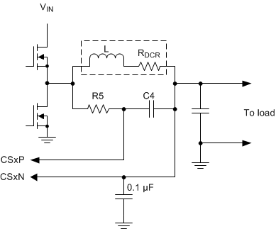 Figure 12. Current Sensing Using DCR
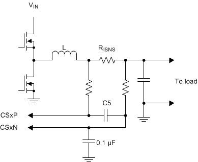 Figure 13. Current Sensing Using Sense Resistor
NOTE
The programming range of current sense element resistance is between 0.244 mΩ and 7.747 mΩ. The IOUT_CAL_GAIN command sets the value of the current sense element resistance. The maximum difference between CSP and CSN is limited to 60 mV by the current-sharing and current-limit circuit. However, under some conditions, the current-monitoring circuit has tighter limits, as follows:
- For sense element resistance between 0.244 mΩ and 0.5795 mΩ, the maximum differential voltage is 24 mV
- For sense element resistance between 0.5795 mΩ and 1.1285 mΩ, the maximum differential voltage is 40 mV
- For sense element resistance higher than 1.1285 mΩ, the maximum differential voltage is 60 mV
During smart-power operation current sense as Figure 14 shows, the design requires local bypass capacitors for the CSxN pin of the TPS40428 device and the REFIN pin of the smart power stage to avoid noise problems. The recommended value of C6 is 100 nF. Refer to the datasheet of the smart power stage for a C7 value. The two current signal traces must be routed as a differential pair on quiet area.
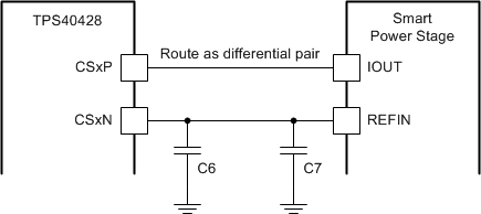 Figure 14. Current Sensing using Smart-Power Stage
NOTE
During smart-power mode operation, the IOUT_CAL_GAIN must be set to 0.5 mΩ.
7.3.8 Temperature Sensing
As shown in Figure 15, the non smart-power operation is selected and ΔVbe measurement of external diode (x3904) is used for temperature sensing. The external diode must be placed close to the inductor if the inductor DCR is used for current sensing, so that the current readout can be more accurate with temperature compensation. It is recommended to place a 1-nF capacitor between the TSNS pin and AGND, and another 1-nF bypass capacitor for the transistor. A separate AGND trace is recommended for the TSNS signal. Route the TSNS trace and the AGND trace as a differential pair.
For temperature sensing using a smart-power stage as shown in Figure 16, the smart-power operation is selected for temperature sensing. Local bypass capacitors are recommended for the TSNS pin of the TPS40428 device and the TAO pin of the smart power stage. The total capacitance of the two bypass capacitors should not exceed 1 nF. The recommended value for both C10 and C11 is 470 pF.
In all cases, the temperature sense trace must be placed in a quiet area and be as short as possible.
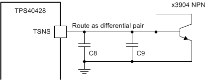 Figure 15. Temperature Sensing Using External Diode
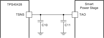 Figure 16. Temperature Sensing Using Smart-Power Stage
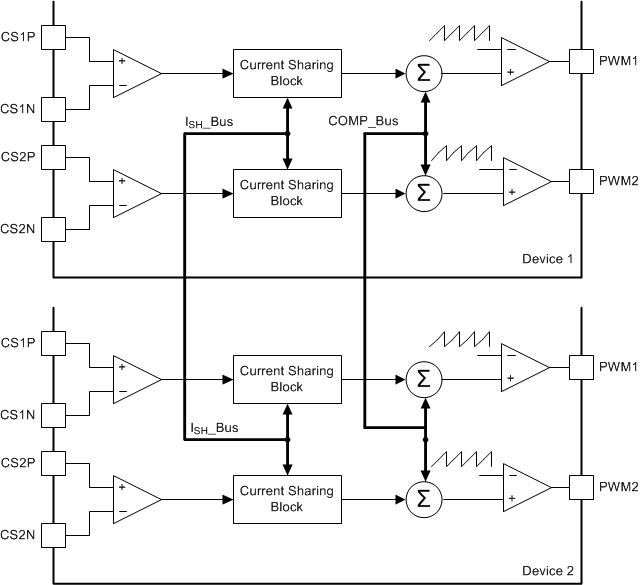
7.3.9 Current Sharing
When the device operates in multi-phase mode, a current sharing loop as shown in Figure 17 maintains the current balance between phases. All phases share the same comparator voltage (VCOMP). The sensed current in each phase is compared first in a current share block, then to an error current and fed into COMP. The resulting error voltage is compared with the voltage ramp to generate the PWM pulse.
7.3.10 Linear Regulators
The TPS40428 device has two on-board linear regulators that provide suitable power for the internal circuitry of the device. These pins, BP3 and BP5 must be properly bypassed to function properly. The BP3 pin requires a minimum capacitance of 0.33 µF connected to AGND and the BP5 pin should have approximately 1 μF of capacitance connected to PGND. The bypass capacitors for VDD, BP5 and BP3 pins need to be placed as close to the device as possible.
7.3.11 Power Sequence Between TPS40428 Device and Power Stage
Before soft-start operation begins to generate a PWM signal, the VDD voltage for power stage must be prepared. Refer to the power stage datasheet for VDD value. Without preparation, the TPS40428 device outputs the PWM signal at maximum duty cycle, because the power stage is not working and output voltage is not regulated.
The VDD voltage for power stage must remain above its threshold until the TPS40428 device is turned off.
7.3.12 PWM Signal
The PWM signal has three voltage levels:
- High level to turn on only the high-side MOSFET
- Level level to turn on only the low-side MOSFET
- Tri-state level to turn off both high-side and low-side MOSFETs.
The PWM pin is open during tri-state, the tri-state level is determined by the resistor-divider network in the power stage or power block. During the transition from any other level to tri-state level, the PWM drivers of the TPS40428 device actively drive the PWM pins to 1.6 V and remain at that level for approximately 20 ns. The PWM pins are then released to allow them return to the voltage level established by the resistor-divider network in the power stage or power block.
7.3.13 Startup and Shutdown
The start-up and shutdown function of the device is controlled by an operation command, control pin or input voltage. Figure 18 shows the TPS40428 device is controlled by both operation command and control pin. A turn-on delay and turn-off delay can be added via PMBus commands.
NOTE
If the device turns off due to a turn-off delay time, any attempt to turn on the device before the turn-off delay time expires should be avoided. The device is available to be turned on only after the turn-off delay time expires and the device has been turned off.
For 3-phase and 4-phase configurations, the turn-on delay of both controllers must be programmed to the same value. The same requirement is for turn-off delay.
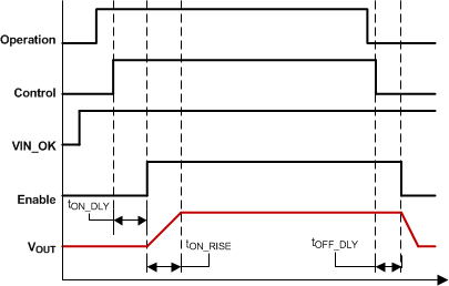 Figure 18. Device Controlled by Both OPERATION and CONTROL
7.3.14 Pre-Biased Output Start-up
This controller supports a pre-biased, output start-up sequence. When the internal, soft-start DAC voltage reaches the FB voltage, the high-side MOSFET gradually turns on.
During soft-start operation, when the PWM pulse width is shorter than the minimum controllable on-time (tON) which is generally caused by the modulator and gate driver delays, pulse skipping may occur and the output might show slightly larger ripple voltage.
7.3.15 PGOOD Indication
The TPS40428 device monitors the voltage on FB pin to indicate whether the output voltage is in regulation or not. During the soft-start sequence, the PG pin is pulled to GND. During operation using factory default settings, after the soft-start time expires, the PG pin releases after a 2-ms delay time if the output voltage is within the PGOOD window (between PG_Low and PG_High). The 2-ms delay can be disabled using the MFR_SPECIFIC_16 register. The PG pin is pulled to ground instantly when the output voltage is below PG_Low or above PG_High.
The PG_Low and PG_High value can be set by the PMBus command MFR_SPECIFIC_07(PCT_VOUT_FAULT_PG_LIMIT).
7.3.16 Overcurrent Protection
The overcurrent protection uses a two-tier approach. Cycle-by-cycle current limit is implemented when the inductor peak current exceeds the set threshold. PMBus sets the current limit using the IOUT_OC_FAULT_LIMIT and IOUT_OC_WARN_LIMIT commands. After a series of seven OC counts, the device turns off both high-side and low-side MOSFETs and enters hiccup mode by default. Only cycle-by-cycle current limit is applied if OC is detected during soft-start operation.
The IOUT_OC_FAULT_RESPONSE PMBus command programs the response to an OC fault. The controller can be programmed to either shut down until power-cycle, CNTLx toggling, or to shut down and attempt restart after a delay of 7 × tON_RISE. When channel 2 is configured as a slave, this command cannot be programmed. In such a case where channel 2 is a slave, the fault response setting for channel 1 is automatically applied to channel 2. For 3-phase and 4-phase configurations, both the controllers must be programmed for the appropriate fault response.
7.3.17 Output Overvoltage/Undervoltage Protection
The TPS40428 device monitors the voltage on FB pin to provide UV and OV protection. The UV threshold is proportional to the reference voltage. The OV threshold is a fixed value in factory default setting and can be a tracking value which is proportional to the reference voltage upon PMBus program.
The UV protection scheme is the same as OC protection scheme. When UV fault is triggered, both high-side and low-side MOSFETs are turned off. The IOUT_OC_FAULT_RESPONSE setting determines the controller response to UV fault. For example, if the IOUT_OC_FAULT_RESPONSE is set to restart the controller after OC fault, then the controller is internally also programmed to restart after a UV fault. UV protection is only detected after soft-start sequence has completed
When an OV fault is triggered, the high-side MOSFET is turned off and the low-side MOSFET remains on to discharge the output. The controller keeps the low-side MOSFET on until VDD power recycle, CNTL pin or command toggling. This behavior protects the output against an overvoltage condition. When the OV threshold is a fixed value, OV protection is active at any time. When the OV threshold is proportional to the reference voltage, OV protection is enabled only after soft-start is done. When operating in multi-phase mode, only the FB pin of the master channel is detected for output voltage UV and OV fault. Output voltage related faults are not detected on any slave channels. Refer to the MFR_SPECIFIC_07 (PCT_VOUT_FAULT_PG_LIMIT) (D7h) and (E0h) MFR_SPECIFIC_16 (COMM_EEPROM_SPARE) sections for more information.
7.3.18 Overtemperature Fault Protection
The over-temperature fault and warning thresholds are programmable for the external temperature sensors. In the case of an over-temperature fault, the detecting channel turns off both high-side and low-side MOSFETs. When the detected temperature cools to less than the turn-off hysteresis level, the channel attempts a restart. More information can be found in the OT_FAULT_LIMIT and OT_WARN_LIMIT command descriptions.
One on-chip temperature sensor monitors the device junction temperature. If the junction temperature of the device reaches the thermal shutdown limit (160°C typical), the PWM output signals are turned off. When the junction temperature cools to the required level (140°C typical), the PWM initiates soft-start as during a normal power-up cycle.
7.3.19 Input Undervoltage Lockout (UVLO)
The input UVLO turn-on and turn-off thresholds are set through PMBus using VIN_ON and VIN_OFF commands. These thresholds must be set for both controllers in 3-phase and 4-phase applications.
7.3.20 Fault Communication
In the case of OC, VIN_UV, VOUT_UV, or OT fault, the FLT pin for the corresponding channel is pulled low internally. In addition, if the FLT pin of any channel is pulled low externally, that channel is shut down and both high-side and low-side MOSFETs are turned off. In 3-phase and 4-phase applications, the FLT pins of all phases of a rail must be connected together. Thus, a fault on any of the phases results in all the phases of that rail to shut down. If programmed to restart after fault, the rail restarts only after each phase on the rail has released the FLT pin.
7.3.21 Fault Protection Summary
Table 2 summarizes the fault protections and associated responses.
Table 2. Fault Protections and Associated Responses
| FAULT | VIN UV | OC | VOUT UV | VOUT OV | OT | OTFI |
|---|---|---|---|---|---|---|
| Fault description | VDD voltage is above VIN_ON then drops below VIN_OFF | The sensed current is above OC fault threshold | FB voltage is below UV threshold. | FB voltage is above OV threshold | The sensed external temperature is above the OT threshold | The on-chip temperature is above junction shutdown threshold |
| Monitoring signal | VDD voltage | Voltage between CSxP and CSxN | FB voltage | FB voltage | External temperature sensed by TSNSx pin | On-chip temperature |
| PWM | Tri-state | Tri-state | Tri-state | Low | Tri-state | Tri-state |
| High-side MOSFET | OFF | OFF | OFF | OFF | OFF | OFF |
| Low-side MOSFET | OFF | OFF | OFF | ON | OFF | OFF |
| Hiccup/Latch | No | Determined by IOUT_OC_FAULT_RESPONSE | Determined by IOUT_OC_FAULT_RESPONSE | Latched | Hiccup after temperature below reset threshold | Hiccup after temperature below reset threshold |
| Before Soft-start | Enabled | Disabled | Disabled | Enabled at Fixed OV,Disabled at Tracking OV | Enabled | Enabled |
| During soft-start | Enabled | Cycle-by-cycle limit | Disabled | Enabled at Fixed OV,Disabled at Tracking OV | Enabled | Enabled |
| After soft-start | Enabled | Enabled | Enabled | Enabled | Enabled | Enabled |
7.4 Device Functional Modes
The TPS40428 device can be configured to operate in dual-output mode or 2-phase mode. It is also stackable up to four phases. Table 3 lists the operating modes that are supported by the TPS40428 device.
Table 3. Operation Modes
| OPERATION MODE | LOCATION | CHANNEL | |
|---|---|---|---|
| Dual-output | Within a single device | CH1 = Master, CH2 = Master | |
| Two-phase | Within a single device | CH1 = Master, CH2 = Slave | |
| Three-phase | Between two devices | IC1 | CH1 = Master, CH2 = Slave2 |
| IC2 | CH1 = Slave1, CH2 = Independent | ||
| Four-phase | Between two devices | IC1 | CH1 = Master, CH2 = Slave2 |
| IC2 | CH1 = Slave1, CH2 = Slave3 | ||
The TPS40428 device uses the remote sense amplifier of master channel to compensate for the parasitic offset to provide an accurate output voltage.
NOTE
In multi-phase operation, FB pins of slave channels must be tied to the BP5 pin of the particular device. The COMP pins of all channels in the same rail are tied together, and ISH pins are tied together, to ensure current sharing between channels. FLT pins are tied together to ensure all channels in the same rail shut down in case a fault occurs on any channel. Refer to Table 4 and Table 5 for detailed information. Ensure that the MFR_SPECIFIC_22 (PWM_OSC_SELECT) (E6h) command is set correctly, to ensure phase shift between phases.
In 3-phase and 4-phase operation, the SYNC pins of two devices are tied together, and PHSET pins of two devices are tied together to ensure phase shift between phases.
7.5 Programming
Figure 19 shows a typical schematic for a 2-phase application. Table 4, Table 5, and Table 6 summarize pin configurations for different applications
During the layout design, route the ISH bus, COMP bus, SYNC bus and PHSET bus as short traces to reduce parasitic inductance and capacitance.
7.5.1 Multi-Phase Applications
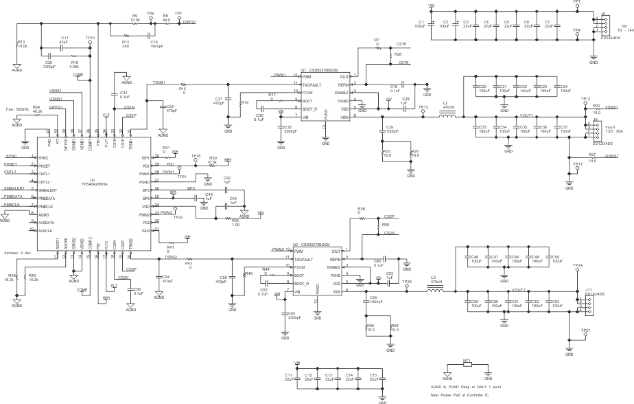 Figure 19. Typical 2-Phase Application Schematic
Table 4. Pin Configurations for Dual Output and 2-Phase Operation
| PIN NAME | DUAL OUTPUT | 2-PHASE |
|---|---|---|
| RT | Connecting a resistor from this pin to AGND | Connecting a resistor from this pin to AGND |
| SYNC | Floating or connect to external clock | Floating or connect to external clock |
| PHSET | Floating | Floating |
| FB1 | Inverting input to the error amplifier 1 | Inverting input to the error amplifier 1 |
| FB2 | Inverting input to the error amplifier 2 | Connect to BP5 |
| COMP1 | Output of the error amplifier 1 | Output of the error amplifier 1, connect to COMP bus |
| COMP2 | Output of the error amplifier 2 | Connect to COMP bus |
| ISH1 | Floating | Connect to ISH bus |
| ISH2 | Floating | Connect to ISH bus |
| FLT1 | Fault inductor of CH1 | Connect to FLT bus |
| FLT2 | Fault inductor of CH2 | Connect to FLT bus |
| PG1 | Power good indicator for CH1 output voltage, connect to BP5 via a pull-up resistor | Power good indicator for 2-phase output voltage, connect to BP5 via a pull-up resistor |
| PG2 | Power good indicator for CH2 output voltage, connect to BP5 via a pull-up resistor | Floating or connect to GND |
| VSENS1 | Positive pin of Voltage Sense Signal for CH1 | Positive pin of Voltage Sense Signal for 2-phase output |
| GSENS1 | Negative pin of Voltage Sense Signal for CH1 | Negative pin of Voltage Sense Signal for 2-phase output |
| VSENS2 | Positive pin of Voltage Sense Signal for CH2 | Connect to GND is recommended. Connect to the output voltage is also allowed. |
| GSENS2 | Negative pin of Voltage Sense Signal for CH2 | Connect to GND |
| CNTL1 | Logic level input which starts or stops CH1 | Logic level input which starts or stops both channels. |
| CNTL2 | Logic level input which starts or stops CH2 | Floating |
| DIFFO1 | Remote Sense Amplifier Output for CH1 | Remote Sense Amplifier Output for 2-phase |
| AVSDATA | AVS data(1) | AVS data for 2-phase(1) |
| AVSCLK | AVS CLOCK(1) | AVS CLOCK for 2-phase(1) |
Table 5. Pin Configurations for 3-Phase and 4-Phase Operation(1)
| DEVICE | PIN NAME | 3-PHASE | 4-PHASE |
|---|---|---|---|
| IC1 (Master) |
RT | Connecting a resistor from this pin to AGND, use the same RT resistor value for IC1 and IC2 | Connecting a resistor from this pin to AGND, use the same RT resistor value for IC1 and IC2 |
| SYNC | Connect to SYNC bus | Connect to SYNC bus | |
| PHSET | Connect to PHSET bus | Connect to PHSET bus | |
| FB1 | Inverting input to the error amplifier 1 of IC1 | Inverting input to the error amplifier 1 of IC1 | |
| FB2 | Connect to BP5 of IC1 | Connect to BP5 of IC1 | |
| COMP1 | Output of the error amplifier 1of IC1, connect to COMP bus | Output of the error amplifier 1 OF IC1, Connect to COMP bus | |
| COMP2 | Connect to COMP bus | Connect to COMP bus | |
| ISH1 | Connect to ISH bus | Connect to ISH bus | |
| ISH2 | Connect to ISH bus | Connect to ISH bus | |
| FLT1 | Connect to FLT bus | Connect to FLT bus | |
| FLT2 | Connect to FLT bus | Connect to FLT bus | |
| PG1 | Power good indicator for 3-phase output voltage, connect to BP5 via a pull-up resistor | Power good indicator for 4-phase output voltage, connect to BP5 via a pull-up resistor | |
| PG2 | Floating or connect to GND | Floating or connect to GND | |
| VSENS1 | Positive pin of Voltage Sense Signal for 3-phase output | Positive pin of Voltage Sense Signal for 4-phase output | |
| GSENS1 | Negative pin of Voltage Sense Signal for 3-phase output | Negative pin of Voltage Sense Signal for 4-phase output | |
| VSENS2 | Connect to GND is recommended. Connect to the output voltage is also allowed. | Connect to GND is recommended. Connect to the output voltage is also allowed. | |
| GSENS2 | Connect to GND | Connect to GND | |
| CNTL1 | Logic level input which starts or stops 3-phase | Logic level input which starts or stops 4-phase | |
| CNTL2 | Floating | Floating | |
| DIFFO1 | Remote Sense Amplifier Output for 3-phase | Remote Sense Amplifier Output for 4-phase | |
| AVSDATA | AVS data for 3-phase(1) | AVS data for 4-phase(1) | |
| AVSCLK | AVS CLOCK for 3-phase(1) | AVS CLOCK for 4-phase(1) | |
| IC2 (Slave) |
RT | Connecting a resistor from this pin to AGND, use the same RT resistor value for IC1 and IC2 | Connecting a resistor from this pin to AGND, use the same RT resistor value for IC1 and IC2 |
| SYNC | Connect to SYNC bus | Connect to SYNC bus | |
| PHSET | Connect to PHSET bus | Connect to PHSET bus | |
| FB1 | Connect to BP5 of IC2 | Connect to BP5 of IC2 | |
| FB2 | Inverting input to the error amplifier 2 of IC2 | Connect to BP5 of IC2 | |
| COMP1 | Connect to COMP bus | Connect to COMP bus | |
| COMP2 | Output of the error amplifier 2 of IC2 | Connect to COMP bus | |
| ISH1 | Connect to ISH bus | Connect to ISH bus | |
| ISH2 | Floating | Connect to ISH bus | |
| FLT1 | Connect to FLT bus | Connect to FLT bus | |
| FLT2 | Fault indicator for CH2 of IC2 | Connect to FLT bus | |
| PG1 | Floating or connect to GND | Floating or connect to GND | |
| PG2 | Power good indicator for CH2 output voltage of IC2, connect to BP5 via a pull-up resistor | Floating or connect to GND | |
| VSENS1 | Connect to GND is recommended. Connection to the output voltage is also allowed. | Connect to GND is recommended. Connection to the output voltage is also allowed. | |
| GSENS1 | Connect to GND | Connect to GND | |
| VSENS2 | Positive pin of Voltage Sense Signal for CH2 of IC2 | Connect to GND is recommended. Connect to the output voltage is also allowed. | |
| GSENS2 | Negative pin of Voltage Sense Signal for CH2 of IC2 | Connect to GND | |
| CNTL1 | Connect to CNTL1 of IC1 | Connect to CNTL1 of IC1 | |
| CNTL2 | Logic level input which starts or stops CH2 of IC2 | Floating | |
| DIFFO1 | Floating | Floating | |
| AVSDATA | Can be used for CH2 of IC2.(1) | See (1) | |
| AVSCLK | Can be used for CH2 of IC2.(1) | See (1) |
Table 6. Configurations of Unused Pins
7.6 Register Maps
7.6.1 PMBus General Description
Timing and electrical characteristics of the PMBus can be found in the PMB Power Management Protocol Specification, Part 1, revision 1.1 available at http://PMBus.org. The TPS40428 device supports both the 100-kHz and 400-kHz bus timing requirements. The TPS40428 device does not stretch pulses on the PMBus when communicating with the master device.
Communication over the TPS40428 device PMBus interface can support the packet error checking (PEC) scheme if desired. If the master supplies CLK pulses for the PEC byte, PEC is used. If the CLK pulses are not present before a STOP, the PEC is not used.
The TPS40428 device supports a subset of the commands in the PMBus 1.1 specification. Most of the controller parameters can be programmed using the PMBus and stored as defaults for later use. All commands that require data input or output use the literal format. The exponent of the data words is fixed at a reasonable value for the command and altering the exponent is not supported. Direct format data input or output is not supported by the TPS40428 device. See the Supported PMBus Commands section for specific details.
The TPS40428 device also supports the SMBALERT response protocol. The SMBALERT response protocol is a mechanism by which a slave (the TPS40428 device) can alert the bus master that it wants to talk. The master processes this event and simultaneously accesses all slaves on the bus (that support the protocol) through the alert response address. Only the slave that caused the alert acknowledges this request. The host performs a modified receive byte operation to get the slave’s address. At this point, the master can use the PMBus status commands to query the slave that caused the alert. For more information on the SMBus alert response protocol, see the System Management Bus (SMBus) specification.
The TPS40428 device contains non-volatile memory that is used to store configuration settings and scale factors. The settings programmed into the device are not automatically saved into this non-volatile memory though. The STORE_USER_ALL command must be used to commit the current settings to non-volatile memory as device defaults. The settings that are capable of being stored in non-volatile memory are noted in their detailed descriptions.
7.6.2 PMBus Functionality
7.6.2.1 PMBus Address
The PMBus specification requires that each device connected to the PMBus have a unique address on the bus. The TPS40428 device has 64 possible addresses (0 through 63 in decimal) that can be assigned by connecting resistors from the ADDR0 and ADDR1 pins to AGND. The address is set in the form of two octal (0-7) digits, one digit for each pin. ADDR1 is the high-order digit an ADDR0 is the low-order digit.
During PMBus communication, the PMBus address of the TPS40428 device is the concatenation of '0b'+ADDR1+ADDR0. The R/W bit of PMBus protocol is added at the end of address to make it net 8-bit wide.
The E96 series resistors suggested for each digit value are shown in Table 7.
Table 7. E96 Series Resistors
| DIGIT | RESISTANCE (kΩ) |
|---|---|
| 0 | 8.45 |
| 1 | 16.2 |
| 2 | 25.5 |
| 3 | 37.4 |
| 4 | 54.9 |
| 5 | 84.5 |
| 6 | 133 |
| 7 | 200 |
The TPS40428 also detects values that are out of range on the ADDR0 and ADDR1 pins. If either pin is detected as having an out of range resistance connected to it, the device continues to respond to PMBus commands, but at address 127, which is outside of the possible programmed addresses. It is possible but not recommended to use the device in this condition, especially if other TPS40428 devices are present on the bus or if another device could possibly occupy the 127 address.
NOTE
Some addresses are reserved by SMBus specification and must not be used by or assigned to SMBus slave device. Refer to SMBus specification for more information.
7.6.2.2 PMBus Connections
The TPS40428 device supports both the 100-kHz and 400-kHz bus speeds. Connection for the PMBus interface should follow the High Power DC specifications given in section 3.1.3 on the System Management Bus (SMBus) Specification V2.0 for the 400-kHz bus speed or the Low Power DC specifications in section 3.1.2. The complete SMBus specification is available from the SMBus website, smbus.org.
7.6.2.3 PMBus Data Format
There are three data formats supported in PMBus form commands that require representation of a literal number as their argument (commands that set thresholds, voltages or report such). A compatible device needs to only support one of these formats. The TPS40428 device supports the linear data format only for these commands. In this format, the data argument consists of two parts, a mantissa and an exponent. The number represented by this argument can be expressed as shown in Equation 5.

7.6.2.4 PMBus Output Voltage Adjustment
The nominal output voltage of the converter can be adjusted using the VREF_TRIM commandSee the MFR_SPECIFIC_04 (VREF_TRIM) (D4h) command description for the format of this command as used in the TPS40428 device. The adjustment range is between –20% and 10% from the nominal output voltage. The VREF_TRIM command is typically used to trim the final output voltage of the converter without relying on high-precision resistors being used in Figure 11. The resolution of the adjustment is 2 mV for each step. The nominal output for margining and VREF_TRIM remains limited to between –30% and 10%. Exceeding this range is not supported.
The TPS40428 device operates in three states that determine the actual output voltage:
- No output margin
- Margin high
- Margin low
7.6.2.4.1 No Margin Voltage

7.6.2.4.2 Margin High Voltage State

7.6.2.4.3 Margin Low State

where
- VFB is the FB pin voltage
- VREF_TRIM is the offset voltage in volts to be applied to the output voltage
- VREF_MARGIN_HIGH is the requested margin high voltage
- VREF_MARGIN_LOW is the requested margin low voltage
7.6.2.5 Reading the Output Current
The average output current for the converter is readable using the READ_IOUT command. The results of this command support only positive or current sourced from the converter. If the converter is sinking current the result of this command is a reading of 0 A.
7.6.2.6 Soft-Start Time
The TPS40428 device supports several soft-start times from 600 μs to 9 ms selected by the TON_RISE PMBus command. See the command description for full details on the levels and implementation. When selecting the soft-start time, ensure that the charging current for the output capacitors is carefully considered. In some applications (for example, those with large amounts of output capacitance) this current can lead to problems with nuisance tripping of the overcurrent protection circuitry. To ensure that these problems do not happen, the output capacitor charging current should be included when considering where to set the overcurrent threshold. The output capacitor charging current can be found using Equation 9:
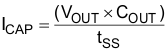
where
- ICAP is the startup charging current of the output capacitance in A
- VOUT is the output voltage of the converter in V
- COUT is the total output capacitance in F
- tSS is the selected soft-start time in seconds
With the charging current calculated, the overcurrent threshold can then be calibrated to the sum of the maximum load current and the output capacitor charging current plus some margin. The amount of margin required depends on the individual application, but 25% is a suggested starting point. More or less may be required.
NOTE
For 3-phase and 4-phase configurations, the soft-start time of both controllers must be programmed to the same value.
7.6.2.7 Turn-On/Turn-Off Delay and Sequencing
The TPS40428 device provides many sequencing options. Using the ON_OFF_CONFIG command, each rail can be configured to start-up whenever the input is not in undervoltage lockout or to additionally require a signal on the CNTLx pin and/or receive an update to the OPERATION command over PMBus.
When the gating signal as specified by ON_OFF_CONFIG is reached for that rail, a programmable turn-on delay can be set with TON_DELAY. The rise time can be programmed with TON_RISE. When the specified signal(s) are set to turn the output off, a programmable turn-off delay set by TOFF_DELAY is used before switching is inhibited. More information can be found in the PMBus command descriptions.
When the output voltage is within the PGOOD limits after the start-up period, the PGOOD pin is asserted. This can be connected to the CNTL pin of another rail in dual-output mode or on another device to control turn-on and turn-off sequencing.
7.6.2.8 Supported PMBus Commands
The TPS40428 device supports the following commands from the PMBus 1.1 specification.
Table 8. PMBus Factory Default Setting
| CODE | COMMAND NAME | WORD/BYTE | DESCRIPTION: PMBus Command | USER WRITABLE |
FACTORY DEFAULT VALUE |
|---|---|---|---|---|---|
| 00h | PAGE | Byte | Locates separate PMBus command lists in multiple output environments | Yes | 0XXX XXX0 |
| 01h | OPERATION | Byte | Turn the unit on and off in conjunction with the input from the CONTROL pin. Set the output voltage to the upper or lower MARGIN VOLTAGES. | Yes | 0X00 00XX |
| 02h | ON_OFF_CONFIG | Byte | Configures the combination of CONTROL pin input and serial bus commands needed to turn the unit on and off. This includes how the unit responds when power is applied. | Yes | XXX1 0110 |
| 03h | CLEAR_FAULTS | Byte | Clears all fault status registers to 0x00. The "Unit is Off" bit in the status byte is not cleared when this command is issued. | Yes(1) | NONE |
| 10h | WRITE_PROTECT | Byte | Prevents unwanted writes to the device. | Yes | 000X XXXX |
| 15h | STORE_USER_ALL | Byte | Saves the current configuration into the User Store. Note: This command writes to Non-Volatile Memory. | Yes(1) | NONE |
| 16h | RESTORE_USER_ALL | Byte | Restores all parameters to the settings saved in the User Store. | Yes(1) | NONE |
| 19h | CAPABILITY | Byte | PEC,SPD,ALRT | No | 1011 0000 |
| 20h | VOUT_MODE | Byte | Read-Only Mode Indicator. The data format is linear with an exponent of -9 | No | 0001 0111 |
| 35h | VIN_ON | Word | Sets the value of the input voltage at which the unit should start power conversion | Yes | 1111 0000 0001 0001 |
| 36h | VIN_OFF | Word | Sets the value of the input voltage at which the unit should stop power conversion. | Yes | 1111 0000 0001 0000 |
| 38h | IOUT_CAL_GAIN | Word | Sets the ratio of the voltage at the current sense pins to the sensed current. | Yes | 1000 0000 0010 0001 |
| 39h | IOUT_CAL_OFFSET | Word | Nulls any offsets in the output current sensing circuit. | Yes | 1110 0000 0000 0000 |
| 46h | IOUT_OC_FAULT_LIMIT | Word | Sets the value of the output current, in amperes, that causes the overcurrent detector to indicate an overcurrent fault condition. | Yes | 1111 1000 0101 0000 |
| 47h | IOUT_OC_FAULT_RESPONSE | Byte | Instructs the device on what action to take in response to an output overcurrent fault. | Yes | 0011 1111 |
| 4Ah | IOUT_OC_WARN_LIMIT | Word | Sets the value of the output current that casues an output overcurrent warning. | Yes | 1111 1000 0100 1010 |
| 4Fh | OT_FAULT_LIMIT | Word | Overtemperature fault threshold | Yes | 0000 0000 1001 0001 |
| 5Ih | OT_WARN_LIMIT | Word | Overtemperature warning threshold | Yes | 0000 0000 0111 1101 |
| 61h | TON_RISE | Word | Target soft-start rise time | Yes | 1110 0000 0010 1011 |
| 78h | STATUS_BYTE | Byte | Single byte status indicator | No | 0x00 0000 |
| 79h | STATUS_WORD | Word | Full 2-byte status indicator | No | 0000 0000 0x00 0000 |
| 7Ah | STATUS_VOUT | Byte | Output voltage fault status detail | No | 0000 0000 |
| 7Bh | STATUS_IOUT | Byte | Output current fault status detail | No | 0000 0000 |
| 7Dh | STATUS_TEMPERATURE | Byte | Temperature fault status detail | No | 0000 0000 |
| 7Eh | STATUS_CML | Byte | Communication, memory, and logic fault status detail | No | 0000 0000 |
| 80h | STATUS_MFR_SPECIFIC | Byte | Manufacturer specific fault status detail | No | 0000 0000 |
| 8Bh | READ_VOUT | Word | Read output voltage | No | 0000 0000 0000 0000 |
| 8Ch | READ_IOUT | Word | Read output current | No | 1110 0000 0000 0000 |
| 8Eh | READ_TEMPERATURE_2 | Word | Read off-chip temp sensor | No | 1111 0000 0110 0100 |
| 98h | PMBUS_REVISION | Byte | PMBus Revision Information | No | 0001 0001 |
| D0h | MFR_SPECIFIC_00 | Word | User scratch pad | Yes | 0000 0000 0000 0000 |
| D4h | MFR_SPECIFIC_04 | Word | VREF_TRIM | Yes | 0000 0000 0000 0000 |
| D5h | MFR_SPECIFIC_05 | Word | STEP_VREF_MARGIN_HIGH | Yes | 0000 0000 0001 1110 |
| D6h | MFR_SPECIFIC_06 | Word | STEP_VREF_MARGIN_LOW | Yes | 1111 1111 1110 0010 |
| D7h | MFR_SPECIFIC_07 | Byte | PCT_VOUT_FAULT_PG_LIMIT | Yes | XXXX XX01 |
| D8h | MFR_SPECIFIC_08 | Byte | SWQUENCE_TON_TOFF_DELAY | Yes | 000X 000X |
| E0h | MFR_SPECIFIC_16 | Word | COMM_EEPROM_SPARE | Yes | 1011 0001 xxxx x011 |
| E5h | MFR_SPECIFIC_21 | Word | IC options | Yes | 0111 1111 0000 0000 |
| E6h | MFR_SPECIFIC_22 | Word | PWM_OSC_SELECT | Yes | 0000 0000 0000 0000 |
| E7h | MFR_SPECIFIC_23 | Word | Paged and Common MASK_SMBALERT | Yes | 0000 0000 0000 0000 |
| E9h | MFR_SPECIFIC_25 | Word | AVS_CONFIG | Yes | 0000 0000 0000 0010 |
| EAh | MFR_SPECIFIC_26 | Word | AVS_ADDRESS | Yes | 0000 0000 0000 0101 |
| EBh | MFR_SPECIFIC_27 | Word | AVS_DAC_DEFAULT | Yes | 0000 0001 1111 0100 |
| ECh | MFR_SPECIFIC_28 | Word | AVS_CLAMP_HI | Yes | 0000 0010 1110 1110 |
| EDh | MFR_SPECIFIC_29 | Word | AVS_CLAMP_LO | Yes | 0000 0000 1111 1010 |
| EFh | MFR_SPECIFIC_30 | Word | Temperature offset | Yes | 1111 1000 0000 0000 |
| F0h | MFR_SPECIFIC_32 | Word | API options | Yes | 0000 0000 0000 0000 |
| FCh | MFR_SPECIFIC_44 | Word | Device code, unique code to id part number | No | 0000 0001 1110 0000 |
7.6.2.8.1 PAGE (00h)
| Format | Unsigned binary integer | ||||
| Description | The PAGE command provides the ability to configure, control, and monitor through only one physical address both channels (outputs) of the TPS40428 device. | ||||
| Default | 0XXX XXX0 (binary) | ||||
| PAGE | |||||||
| r/w | r | r | r | r | r | r | r/w |
| 7 | 6 | 5 | 4 | 3 | 2 | 1 | 0 |
| PA | X | X | X | X | X | X | P0 |
| Bits | Field Name | Description |
|---|---|---|
| 7, 0 | PA, P0 | 00: (Default) All commands address the first channel 01: All commands address the second channel 10: Illegal input - ignore this write, take no action 11: All commands address both channels If PAGE = 11, any then read commands point to PAGE0 always. |
| 6:1 | X | X indicates writes are ignored and reads are 0. Any values written to read-only registers are ignored. |
7.6.2.8.2 OPERATION (01h)
| Format | N/A | ||||
| Description | The OPERATION command is used to turn the device output on or off in conjunction with the input from the CNTLx pin (where x = 1 for channel 1 and x = 2 for channel 2). It is also used to set the output voltage to the upper or lower MARGIN levels. OPERATION is a paged register. In order to access OPERATION register for channel 1 of the TPS40428 device, PAGE must be set to 0. In order to access OPERATION register for channel 2 of the TPS40428 device, PAGE must be set to 1. For simultaneous access of channels 1 and 2, PAGE command must be set to 11. If the channel is configured as a SLAVE, this command can not be accessed for that channel. Any writes to the SLAVE channel for this command are ignored. An attempt to read and write the SLAVE channel command results in a NACK’d command and the reporting of an IVC fault and triggering of SMB_ALERT. |
||||
| Default | 0X0000XX (binary) | ||||
| r/w | r | r/w | r/w | r/w | r/w | r | r |
| 7 | 6 | 5 | 4 | 3 | 2 | 1 | 0 |
| On | 0 | Margin | X | X | |||
| Bits | Field Name | Description |
|---|---|---|
| 7 | On | (Format: binary) The On bit is used to enable to IC via PMBus. The necessary condition for this bit to be effective is that the cmd bit in the ON_OFF CONFIG register is set high. However, the cmd bit being high is not a sufficient condition to enable the IC via the On bit, as specified below: 0: (Default) The device output is not enabled via PMBus. 1: The device output is enabled if: a. The supply voltage VIN is greater than the VIN_UVLO threshold, the cmd bit is high, and b. The bit cpr in the ON_OFF CONFIG register is low, or c. The bit cpr is high and the CNTL_EN pin is enabled (high or low). |
| 6 | 0 | X: Default |
| 5:2 | Margin | (Format: binary) If Margin Low is enabled, load the value from the STEP_VREF_MARGIN_LOW command. If Margin High is enabled, load the value from the STEP_VREF_MARGIN_HIGH command. (See PMBus specification for more information) 0000: (Default) Margin Off 0101: Margin Low (Ignore Fault) 0110: Margin Low (Act On Fault) 1001: Margin High (Ignore Fault) 1010: Margin High (Act On Fault) Note: Any values written to read-only registers are ignored. |
| 1:0 | X | XX: Default X indicates writes are ignored and reads are 0. Any values written to read-only registers are ignored. |
7.6.2.8.3 ON_OFF_CONFIG (02h)
| Format | N/A | ||||
| Description | The ON_OFF_CONFIG command configures the combination of CONTROL pin input and serial bus commands needed to turn the unit on and off. ON_OFF_CONFIG is a paged register. In order to access this register for channel 1 of the TPS40428 device, PAGE must be set to 0. In order to access this register for channel 2 of the TPS40428 device , PAGE must be set to 1. For simultaneous access of channels 1 and 2, PAGE command must be set to 11. If the channel is configured as a SLAVE, this command can not be accessed for that channel. Any writes to the SLAVE channel for this command are ignored. An attempt to read and write the SLAVE channel command results in a NACK’d command and the reporting of an IVC fault and triggering of SMB_ALERT. However, note that page 0 (channel 1) fault status bits (and associated smbalert state) should be capable of being cleared by toggling CNTL1 pin even if channel 1 is a slave. If channel 2 is a slave, then CNTL2 pin is disabled but toggling the CNTL1 pin should also clear page 1 (channel 2) fault status bits and related smbalert state. (The is recommendation is to tie together CNTL1 pins of both TPS40428 devices in a multi-phase configuration). |
||||
| Default | XXX10110 (binary) The default power-up state can be changed using the STORE_USER_ALL command. |
||||
| r/wE | r/wE | r/wE | r/wE | r | |||
| 7 | 6 | 5 | 4 | 3 | 2 | 1 | 0 |
| X | X | X | pu | cmd | cpr | pol | cpa |
| Bits | Field Name | Description |
|---|---|---|
| 7:5 | X | X indicates writes are ignored and reads are 0. |
| 4 | pu | (Format: binary) Sets the default to either operate any time power is present or for the on/off to be controlled by CONTROL pin and/or PMBus commands. This bit is used in conjunction with the 'cp', 'cmd', and 'on' bits to determine start up. 0: Device powers up any time power is present regardless of state of the CONTROL pin. 1: (Default) Device does not power up until commanded by the CNTL_EN pin and/or OPERATION command as programmed in bits [3:0] of the ON_OFF_CONFIG register. |
| 3 | cmd | (Format: binary) The cmd bit controls how the device responds to commands received via the serial PMBus. This bit is used in conjunction with the 'cpr', 'pu', and 'on' bits to determine start up. 0: (Default) Device ignores the on bit in the OPERATION command. 1: Device responds to the on bit in the OPERATION command, as explained above. |
| 2 | cpr | (Format: binary) Set the CNTL_EN pin response. This bit is used in conjunction with the 'cmd', 'pu', and 'on' bits to determine start up. The cpr bit being high is a necessary but not sufficient condition to enable the IC via the CNTL_EN pin: 0: Device ignores the CNTL_EN pin, i.e., on/off is controlled only by the OPERATION command 1: (Default) The device output is enabled if: a. The supply voltage VIN is greater than the VIN_UVLO threshold, and the CNTL_EN pin is active (high or low), and b. The bit cmd in the ON_OFF CONFIG register is low, or c. The bit cmd is high and the bit on in the OPERATION register is high. |
| 1 | pol | (Format: binary) Polarity of the CONTROL pin 1: (Default) CONTROL pin is active high 0: CONTROL pin is active low To change this value, the user must change this value in the register, save it to the EEPROM and then reboot the device via power down for the new value to take effect. |
| 0 | cpa | (Format: binary) Sets CONTROL pin action when commanding the unit to turn off. 0: (Default) Use the programmed turn-off delay. Note: Any values written to read-only registers are ignored on write and returns a ‘0’ when read. |
7.6.2.8.4 CLEAR_FAULTS (03h)
| Format | N/A | ||||
| Description | CLEAR_FAULTS is a paged command. In order to issue this command for channel 1 of the TPS40428 device, PAGE must be set to 0. In order to issue this command for channel 2 of the TPS40428 device , PAGE must be set to 1. For simultaneous access of channels 1 and 2, PAGE command must be set to 11. The CLEAR_FAULTS command is used to clear any fault bits that have been set. This command simultaneously clears all bits in all status registers in the selected PAGE. At the same time, the device negates (clears, releases) its SMB_ALERT signal output if the device is asserting the SMB_ALERT signal. The CLEAR_FAULTS command does not cause a unit that has latched off for a fault condition to restart. If the fault is still present when the bit is cleared, the fault bit shall immediately be set again and the host notified by the usual means. |
||||
| Bits | Field Name | Description |
|---|---|---|
| 7:0 | No data bytes are sent, only the command code is sent. |
7.6.2.8.5 WRITE_PROTECT (10h)
| Format | N/A | ||||
| Description | The WRITE_PROTECT command is used to control writing to the PMBus device. The intent of this command is to provide protection against accidental changes. This command is not intended to provide protection against deliberate or malicious changes to a device's configuration or operation. All supported commands may have their parameters read, regardless of the WRITE_PROTECT settings. Note: Valid setting of WRITE_PROTECT[7:5] bits disables the RESTORE_USER_ALL command’s ability to restore EEPROM data to protected PMBus Control/Status Registers (CSRs). However, an EEPROM (via the RESTORE_USER_ALL execution) restores the data to any registers the remain unprotected (either by a valid WRITE_PROTECT[7:5] setting, or by any invalid setting of these bits ). No WRITE_PROTECT[7:5] bit setting affects the Reset-Restore operation. All registers having EEPROM support get updated. Likewise, STORE_USER_ALL command operation remains unaffected. |
||||
| Default | 000XXXXX (binary) The default power-up state can be changed using the STORE_USER_ALL command. |
||||
| r/wE | r/wE | r/wE | |||||
| 7 | 6 | 5 | 4 | 3 | 2 | 1 | 0 |
| bit7 | bit6 | bit5 | X | X | X | X | X |
| Bits | Field Name | Description |
|---|---|---|
| 7 | bit7 | (Format: binary) 0: (Default) See table below. 1: Disable all writes except for the WRITE_PROTECT command. (bit5 and bit6 must be 0 to be valid data) |
| 6 | bit6 | (Format: binary) 0: (Default) See table below. 1: Disable all writes except for the WRITE_PROTECT, OPERATION, and PAGE commands. (bit5 and bit7 must be 0 to be valid data) |
| 5 | bit5 | (Format: binary) 0: (Default) See table below. 1: Disable all writes except for the WRITE_PROTECT, OPERATION, PAGE, and ON_OFF_CONFIG commands. (bit6 and bit7 must be 0 to be valid data) |
| 4:0 | X | X indicates writes are ignored and reads are 0. Note: Any values written to read-only registers are ignored. |
|
Invalid data written to WRITE_PROTECT[7:5] causes the ’cml’ bit in the STATUS_BYTE and the ‘ivd’ bit in the STATUS_CML registers to be set. INVALID DATA ALSO RESULTS IN NO WRITE PROTECTION (WRITE_PROTECT = 00h)! |
||
| Data Byte Value | Action |
|---|---|
| 1000 0000 | Disables all WRITES except to the WRITE_PROTECT command. |
| 0100 0000 | Disables all WRITES except to the WRITE_PROTECT, OPERATION, and PAGE commands. |
| 0010 0000 | Disables all WRITES except to the WRITE_PROTECT, OPERATION, PAGE, and ON_OFF_CONFIG commands. |
7.6.2.8.6 STORE_USER_ALL (15h)
| Format | N/A | ||||
| Description | Store all of the current storable register settings in the EEPROM memory as the new defaults on power up. It is permitted to use the STORE_USER_ALL command while the device is operating. However, the device may be unresponsive during the write operation with unpredictable memory storage results. It is recommended to turn the device output off before issuing this command. EEPROM programming faults set the ‘cml’ bit in the STATUS_BYTE and the ‘oth’ bit in the STATUS_CML registers. |
||||
7.6.2.8.7 RESTORE_USER_ALL (16h)
| Format | N/A | ||||
| Description | Write EEPROM data to those registers which: (1) have EEPROM support, and; (2) are unprotected according to current setting of the WRITE_PROTECT[7:5] bits. It is permitted to use the RESTORE_USER_ALL command while the device is operating. However, the device may be unresponsive during the copy operation with unpredictable, undesirable or even catastrophic results. It is recommended to turn the device output off before issuing this command. |
||||
| Bits | Field Name | Description |
|---|---|---|
| 7:0 | No data bytes are sent, only the command code is sent. |
7.6.2.8.8 CAPABILITY (19h)
| Format | N/A | ||||
| Description | This command provides a way for a host system to determine some key capabilities of this PMBus device. | ||||
| Default | 10110000 (binary) | ||||
| r | r | r | r | r | r | r | r |
| 7 | 6 | 5 | 4 | 3 | 2 | 1 | 0 |
| PEC | SPD | ALRT | Reserved | ||||
| Bits | Field Name | Description |
|---|---|---|
| 7 | PEC | (Format: binary) Packet Error Checking is supported. 1: Default Note: Any values written to read-only registers are ignored. |
| 6:5 | SPD | (Format: binary) Maximum supported bus speed is 400 kHz. 01: Default Note: Any values written to read-only registers are ignored. |
| 4 | ALRT | (Format: binary) This device does have a SMB_ALERT pin and does support the SMBus Alert Response Protocol. 1: Default Note: Any values written to read-only registers are ignored. |
| 3:0 | Reserved | Reserved bits. 0000: Default |
7.6.2.8.9 VOUT_MODE (20h)
| Format | N/A | ||||
| Description | The PMBus specification dictates that the data word for the VOUT_MODE command is one byte that consists of a 3-bit Mode and 5-bit parameter, as shown below. If a host sends a VOUT_MODE writer command, the device rejects the VOUT_MODE command, declare a communication fault for invalid data and respond as described in PMBus specification II section 10.2.2. |
||||
| Default | 00010111 (binary) | ||||
| r | r | r | r | r | r | r | r |
| 7 | 6 | 5 | 4 | 3 | 2 | 1 | 0 |
| Mode | Exponent | ||||||
| Bits | Field Name | Description |
|---|---|---|
| 7:5 | Mode | (Format: binary) 000: (Default) Linear Format |
| 4:0 | Exponent | (Format: two's complement binary) 10111: (Default) Exponent value = –9 Note: Any values written to read-only registers are ignored. |
7.6.2.8.10 VIN_ON (35h)
The VIN_ON command sets the value of the input voltage at which the unit should start power conversion assuming all other conditions are met.
Values written within the supported VIN range are mapped to the nearest supported increment.
The supported VIN_ON values are:
| 4.25 (default) | 4.5 | 4.75 | 5 | 5.25 | 5.5 | 5.75 |
| 6 | 6.25 | 6.5 | 6.75 | 7 | 7.25 | 7.5 |
| 7.75 | 8 | 8.25 | 8.5 | 8.75 | 9 | 9.25 |
| 9.5 | 10 | 10.5 | 11 | 11.5 | 12 | 12.5 |
| 13 | 14 | 15 | 16 | |||
| Format | Linear | ||||
| Description | Attempts to write values outside of the acceptable range are treated as invalid data – in effect, the ’cml’ bit in the STATUS_BYTE register and the ‘ivd’ bit in the STATUS_CML register are set, and SMB_ALERT asserted. Additionally, the value of VIN_ON remains unchanged. Maintaining values within “acceptable range” also indicates that writes to VIN_ON should not attempt to set its value less than that of VIN_OFF. | ||||
| Default | The default setting results in a real VIN_ON of 4.25 V The default power-up state can be changed using the STORE_USER commands. |
||||
| r | r | r | r | r | r | r | r | r | r/wE | r/wE | r/wE | r/wE | r/wE | r/wE | r/wE |
| 7 | 6 | 5 | 4 | 3 | 2 | 1 | 0 | 7 | 6 | 5 | 4 | 3 | 2 | 1 | 0 |
| Exponent | Mantissa | ||||||||||||||
| Bits | Field Name | Description |
|---|---|---|
| 7:3 | Exponent | (Format: two's complement) This is the exponent for the linear format. Default: 11110 (bin) –2 (dec) (equivalent LSB = 0.25 V) These default settings are not programmable. Note: Any values written to read-only registers are ignored. |
| 2:0 7:0 |
Mantissa | (Format: two's complement) This is the Mantissa for the linear format. Default: 000 0001 0001 (bin) 17 (dec) (equivalent VIN_ON voltage = 4.25 V) Minimum: 000 0001 0001 (bin) 17 (dec) (equivalent VIN_ON voltage = 4.25 V) Maximum: 000 0100 0000 (bin) 64 (dec) (equivalent VIN_ON voltage = 16 V) Note: Any values written to read-only registers are ignored. |
7.6.2.8.11 VIN_OFF (36h)
The VIN_OFF command sets the value of the input voltage at which the unit should stop power conversion.
Values written within the supported VIN range are mapped to the nearest supported increment.
The supported VIN_ON values are:
| 4 (default) | 4.25 | 4.5 | 4.75 | 5 | 5.25 | 5.5 |
| 5.75 | 6 | 6.25 | 6.5 | 6.75 | 7 | 7.25 |
| 7.5 | 7.75 | 8 | 8.25 | 8.5 | 8.75 | 9 |
| 9.25 | 9.75 | 10.25 | 10.75 | 11.25 | 11.75 | 12.25 |
| 12.75 | 13.75 | 14.75 | 15.75 |
| Format | Linear | ||||
| Description | Attempts to write values outside of the acceptable range are treated as invalid data – in effect, the ‘cml’ bit in the STATUS_BYTE register and the ‘ivd’ bit in the STATUS_CML register are set, and SMB_ALERT asserted. Additionally, the value of VIN_OFF remains unchanged. Maintaining values within “acceptable range” also indicates that writes to VIN_OFF should not attempt to set its value equal to or higher than that of VIN_ON. | ||||
| Default | The default setting results in a real VIN_OFF of 4 V The default power-up state can be changed using the STORE_USER commands. |
||||
| r | r | r | r | r | r | r | r | r | r/wE | r/wE | r/wE | r/wE | r/wE | r/wE | r/wE |
| 7 | 6 | 5 | 4 | 3 | 2 | 1 | 0 | 7 | 6 | 5 | 4 | 3 | 2 | 1 | 0 |
| Exponent | Mantissa | ||||||||||||||
| Bits | Field Name | Description |
|---|---|---|
| 7:3 | Exponent | (Format: two's complement) This is the exponent for the linear format. Default: 11110 (bin) –2 (dec) These default settings are not programmable. Note: Any values written to read-only registers are ignored. |
| 2:0 7:0 |
Mantissa | (Format: two's complement) This is the linear format Mantissa. Default: 000 0001 0000 (bin) 16 (dec) (equivalent VIN_OFF voltage = 4 V) Minimum: 000 0001 0000 (bin) 16 (dec) (equivalent VIN_OFF voltage = 4 V) Maximum: 000 0011 1111 (bin) 63 (dec) (equivalent VIN_OFF voltage = 15.75 V) Note: Any values written to read-only registers are ignored. |
7.6.2.8.12 IOUT_CAL_GAIN (38h)
| Format | Linear | ||||
| Description | The IOUT_CAL_GAIN is the ratio of the voltage at the current sense element to the sensed current. The units are ohms. The effective current sense element is the DCR of the inductor. The default setting is 0.5 mΩ. The resolution is 15.26 µΩ. The range is 0.244 to 7.747 mΩ. When the TPS40428 device operates with TI power stage CSD95378B the IOUT_CAL_GAIN needs to be set to 0.5 mΩ for correct current readout. With regards to multi-phase operation: The user can always write to PAGE 0 (channel 1). PAGE 1 (channel 2) can be written only if it is a master (in effect, the user can not write PAGE 1 if it is configured as a slave). In this case where PAGE 1 is a slave, the PAGE 0 value is used for PAGE1/channel 2. Additionally, for 3-phase or 4-phase mode, the second IC PAGE 0 slave must be programmed by the user to have the same limit value as the master in IC 1 (in effect, the burden is on the user and can not be enforced by the hardware). An attempt to write a PAGE 1 SLAVE channel command results in a NACK’d command and the reporting of an IVC fault and triggering of SMB_ALERT. IOUT_CAL_GAIN is a paged register. In order to access this register for channel 1 of the TPS40428 device, PAGE[7],[0] must be set to 00. In order to access this register for channel 2 of the TPS40428 device , PAGE[7],[0] must be set to 01. For simultaneous access of channels 1 and 2, PAGE[7],[0] command must be set to 11 |
||||
| Default | The default setting results in a real IOUT_CAL_GAIN of 0.5035 mΩ. The default power-up state can be changed using the STORE_USER commands. | ||||
| r | r | r | r | r | r | r | r/wE | r/wE | r/wE | r/wE | r/wE | r/wE | r/wE | r/wE | r/wE |
| 7 | 6 | 5 | 4 | 3 | 2 | 1 | 0 | 7 | 6 | 5 | 4 | 3 | 2 | 1 | 0 |
| Exponent | Mantissa | ||||||||||||||
| Bits | Field Name | Description |
|---|---|---|
| 7:3 | Exponent | (Format: two's complement) This is the exponent for the linear format. Default: 10000 (bin) –16 (dec) (15.26 µΩ) These default settings are not programmable. Note: Any values written to read-only registers are ignored. |
| 2:0 7:0 |
Mantissa | (Format: two's complement) This is the linear format Mantissa. Default: 000 0010 0001 (bin) 32 (dec) (32 × 15.26 µΩ = 0.5035 mΩ) Minimum 016 (dec) = 16 × 15.26 µΩ = 0.244 mΩ Maximum 508 (dec) = 508 × 15.26 µΩ = 7.747 mΩ Note: Any values written to read-only registers are ignored. |
7.6.2.8.13 IOUT_CAL_OFFSET (39h)
| Format | Linear | ||||
| Description | The IOUT_CAL_OFFSET is used to compensate for offset errors in the READ_IOUT command, the IOUT_OC_FAULT_LIMIT command and the IOUT_OC_WARN_LIMIT command. The units are amps. The default setting is 0 A. The resolution is 62.5 mA. The range is 3.9375 A to -4 A. Values outside the valid range are not checked and become aliased into the valid range. For example, 1110 0100 0000 0001 has an expected value of –63.9375 A but results in 1110 0111 1111 0001 which is –3.9375 A. This change occurs because the read-only bits are fixed. The exponent is always –4 and the 5 msb bits of the mantissa are always equal to the sign bit. IOUT_CAL_OFFSET is a paged register. In order to access this register for channel 1 of the TPS40428 device, PAGE[7],[0] must be set to 00. In order to access this register for channel 2 of the TPS40428 controller, PAGE[7],[0] must be set to 01. For simultaneous access of channels 1 and 2, PAGE[7],[0] command must be set to 11. With regards to multi-phase operation: The user can always write to PAGE 0 (channel 1). PAGE 1 (channel 2) can be written only if it is a master (i.e. the user can not write PAGE 1 if it is configured as a slave). In this case where PAGE 1 is a slave, the PAGE0 value are used for PAGE1/channel 2. Additionally, for 3-phase or 4-phase mode, the second IC PAGE 0 slave must be programmed by the user to have the same limit value as the master in IC 1 (in effect, the burden is on the user and can not be enforced by the hardware). An attempt to write a PAGE 1 SLAVE channel command results in a NACK’d command and the reporting of an IVC fault and triggering of SMB_ALERT. |
||||
| Default | The default power-up state can be changed using the STORE_USER commands. | ||||
| r | r | r | r | r | r/wE | r* | r* | r* | r* | r/wE | r/wE | r/wE | r/wE | r/wE | r/wE |
| 7 | 6 | 5 | 4 | 3 | 2 | 1 | 0 | 7 | 6 | 5 | 4 | 3 | 2 | 1 | 0 |
| Exponent | Mantissa | ||||||||||||||
| Bits | Field Name | Description |
|---|---|---|
| 7:3 | Exponent | (Format: two's complement) This is the exponent for the linear format. Default: 11100 (bin) –4 (dec) (lsb = 62.5 mA) These default settings are not programmable. Note: Any values written to read-only registers are ignored. |
| 2:0 7:0 |
Mantissa | (Format: two's complement) This is the linear format Mantissa. Default: 0 (bin) 0 (dec) Bits 1:0, and 7:6 changes for sign extension but are not otherwise programmable Note: Any values written to read-only registers are ignored. |
7.6.2.8.14 IOUT_OC_FAULT_LIMIT (46h)
| Format | Literal | ||||
| Description | The IOUT_OC_FAULT_LIMIT command sets the value of the output current, in amperes, that causes the over-current detector to indicate an over-current fault condition. The IOUT_OC_FAULT_LIMIT should always be set to equal to or greater than the IOUT_OC_WARN_LIMIT. Writing a value to IOUT_OC_FAULT_LIMIT less than IOUT_OC_WARN_LIMIT causes the device to set the ’cml’ bit in the STATUS_BYTE register and the ‘ivd’ bit in the STATUS_CML registers and assert SMB_ALERT.
IOUT_OC_FAULT_LIMIT is a paged register. In order to access this register for channel 1 of the TPS40428 device, PAGE must be set to 0. In order to access this register for channel 2 of the TPS40428 controller, PAGE must be set to 1. For simultaneous access of channels 1 and 2, PAGE command must be set to 11 With regards to multi-phase operation: The user can always write to PAGE 0 (channel 1). PAGE 1 (channel 2) can be written only if it is a master (in effect, the user can not write PAGE 1 if it is configured as a slave). In this case where PAGE 1 is a slave, the PAGE0 value is used for PAGE1/channel 2. Additionally, for 3-phase or 4-phase mode, the second IC PAGE 0 slave must be programmed by the user to have the same limit value as the master in IC 1 (in effect, the burden is on the user and can not be enforced by the hardware). An attempt to write a PAGE 1 SLAVE channel command results in a NACK’d command and the reporting of an IVC fault and triggering of SMB_ALERT. |
||||
| Default | 1111 1000 0101 0000 (binary) The default setting results in a real IOUT_OC_FAULT_LIMIT of 40 A. The default power-up state can be changed using the STORE_USER commands. |
||||
| r | r | r | r | r | r | r | r | r | r/wE | r/wE | r/wE | r/wE | r/wE | r/wE | r/wE |
| 7 | 6 | 5 | 4 | 3 | 2 | 1 | 0 | 7 | 6 | 5 | 4 | 3 | 2 | 1 | 0 |
| Exponent | Mantissa | ||||||||||||||
| Bits | Field Name | Description |
|---|---|---|
| 7:3 | Exponent | (Format: two's complement) This is the exponent for the linear format. Default: 11111 (bin) -1 (dec) (0.5 A) These default settings are not programmable. Note: Any values written to read-only registers are ignored. |
| 2:0 7:0 |
Mantissa | (Format: two's complement) Default: 000 0101 0000 (bin) 80 (dec) (equivalent analog OC = 40 A) Minimum: 000 0000 0110 (bin) 6 (dec) (equivalent analog OC = 3 A) Maximum: 000 0110 0100 (bin) 100 (dec) (equivalent analog OC = 50 A) Note: Any values written to read-only registers are ignored. |
7.6.2.8.15 IOUT_OC_FAULT_RESPONSE (47h)
| Format | Unsigned binary | ||||
| Description | The IOUT_OC_FAULT_RESPONSE command instructs the device on what action to take in response to an IOUT_OC_FAULT_LIMIT or a VOUT under-voltage (UV) fault. When an OC fault is triggered, the device also: • Sets the OCF bit in the STATUS_BYTE register • Sets the OCFW and OCF bits in the STATUS_WORD register • Sets the OCF and OCW bits in the STATUS_IOUT register • Asserts SMB_ALERT, and notifies the host as described in section 10.2.2 of the PMBus Specification. Bits [2:0] are hard-wired to 0x7 (3’b111) to indicate the 7 × Soft-start time delay units in response to an over current or Vout undervoltage fault. IOUT_OC_FAULT_RESPONSE is a paged register. In order to access this register for channel 1 of the TPS40428 device, PAGE must be set to 0. In order to access this register for channel 2 of the TPS40428 device , PAGE must be set to 1. For simultaneous access of channels 1 and 2, PAGE command must be set to 11. With regards to multi-phase operation: The user can always write to PAGE 0 (channel 1). PAGE 1 (channel 2) can be written only if it is a master (in effect, the user can not write PAGE 1 if it is configured as a slave). In this case where PAGE 1 is a slave, the PAGE0 value is used for PAGE1/channel 2. Additionally, for 3-phase or 4-phase mode, the second IC PAGE 0 slave must be programmed by the user to have the same limit value as the master in IC 1 (in effect, the burden is on the user and can not be enforced by the hardware). An attempt to write a PAGE 1 (channel 2) SLAVE channel command results in a NACK’d command and the reporting of an IVC fault and triggering of SMB_ALERT. |
||||
| Default | 00111111 (binary) The default power-up state can be changed using the STORE_USER commands. |
||||
| r | r | r/wE | r/wE | r/wE | r | r | r |
| 7 | 6 | 5 | 4 | 3 | 2 | 1 | 0 |
| 0 | 0 | RS[2] | RS[1] | RS[0] | 1 | 1 | 1 |
| Bits | Field Name | Description |
|---|---|---|
| 7:6 | 0 | Default: XX (X indicates writes are ignored and reads are 0) Note: Any values written to read-only registers are ignored. |
| 5:3 | RS[2:0] | (Format: binary) Output over current retry setting 000: A zero value for the Retry Setting indicates that the unit does not attempt to restart. The output remains disabled until the fault is cleared (See section 10.7 of the PMBus spec.) 111: (Default) A one value for the Retry Setting indicates that the unit goes through a normal startup (Wait → SoftStart) continuously, without limitation, until it is commanded off or bias power is removed or another fault condition causes the unit to shutdown. Any value other than 000 or 111 is not accepted, such and attempt causes the ’cml’ bit in the STATUS_BYTE register and the ‘ivd’ bit in the STATUS_CML register to be set, and SMB_ALERT to be asserted. |
| 2:0 | 1 | Default: xxx (x indicates writes are ignored and reads are 1) Note: Any values written to read-only registers are ignored. |
7.6.2.8.16 IOUT_OC_WARN_LIMIT (4Ah)
| Format | Literal (5-bit two's complement exponent, 11-bit two's complement mantissa) | ||||
| Description | The IOUT_OC_WARN_LIMIT command sets the value of the output current, in amperes, that causes the over-current detector to indicate an over-current warning condition by setting the OCW in bit-5 of the STATUS_IOUT register. • Sets the OTHER bit in the STATUS_BYTE register • Sets the OCFW bit in the STATUS_WORD register • Set the OCW bit in the STATUS_IOUT register • Notifies the host (Asserts SMB_ALERT) IOUT_OC_WARN_LIMIT is a paged register. In order to access this register for channel 1 of the TPS40428 device, PAGE must be set to 0. In order to access this register for channel 2 of the TPS40428 controller, PAGE must be set to 1. For simultaneous access of channels 1 and 2, PAGE command must be set to 11. With regards to multi-phase operation: PAGE 0 can always be written to. PAGE 1 can be written only if it is a master (in effect, you can not write PAGE 1 if it is configured as a slave). In this case where PAGE 1 is a slave, the PAGE0 value is used for PAGE1/channel 2. Additionally, for 3-phase or 4-phase mode, the second IC PAGE 0 slave must be programmed by the user to have the same limit value as the master in IC 1 (in effect, the burden is on the user and can not be enforced by the hardware). An attempt to write a PAGE 1 SLAVE channel command results in a NACK’d command and the reporting of an IVC fault and triggering of SMB_ALERT. The IOUT_OC_WARN_LIMIT should always be set to less than or equal to the IOUT_OC_FAULT_LIMIT. Writing a value to IOUT_OC_WARN_LIMIT greater than IOUT_OC_FAULT_LIMIT causes the device to set the ’cml’ bit in the STATUS_BYTE register and the ‘ivd’ bit in the STATUS_CML registers and assert SMB_ALERT. |
||||
| Default | 1111 1000 0100 1010 (binary) The default setting results in a real IOUT_OC_WARN_LIMIT of 37 A. The default power-up state can be changed using the STORE_USER commands. |
||||
| r | r | r | r | r | r | r | r | r | r/wE | r/wE | r/wE | r/wE | r/wE | r/wE | r/wE |
| 7 | 6 | 5 | 4 | 3 | 2 | 1 | 0 | 7 | 6 | 5 | 4 | 3 | 2 | 1 | 0 |
| Exponent | Mantissa | ||||||||||||||
| Bits | Field Name | Description |
|---|---|---|
| 7:3 | Exponent | (Format: two's complement) This is the exponent for the linear format. Default: 11111 (bin) –1 (dec) (0.5 A) These default settings are not programmable. Note: Any values written to read-only registers are ignored. |
| 2:0 7:0 |
Mantissa | (Format: two's complement) This is the Mantissa for the linear format. Output over current retry setting Default: 000 0100 1010 (bin) 74 (dec) (analog OC Warning = 37 A) Minimum: 000 0000 0100 (bin) 4 (dec) (equivalent analog OC = 2 A) Maximum: 000 0110 0010 (bin) 98 (dec) (equivalent analog OC = 49 A) Note: Any values written to read-only registers are ignored. |
7.6.2.8.17 OT_FAULT_LIMIT (4Fh)
| Format | Literal (5-bit two's complement exponent, 11-bit two's complement mantissa) | ||||
| Description | The OT_FAULT_LIMIT command sets the value of the temperature limit, in degrees Celsius, that causes an over-temperature fault condition when the sensed temperature from the external sensor exceeds this limit. Upon triggering the over-temperature fault, the following actions are taken: • Set the OTFW bit in the STATUS_BYTE register and STATUS_WORD register • Set the OTF and OTW bits in the STATUS_TEMPERATURE register • Notify the host (Asserts SMB_ALERT) • Generate internal signal/s CHx_TSD that eventually shut down the gate drivers. OT_FAULT_LIMIT is a paged register. In order to access this register for channel 1 of the TPS40428 device, PAGE must be set to 0. In order to access this register for channel 2 of the TPS40428 device , PAGE must be set to 1. For simultaneous access of channels 1 and 2, PAGE command must be set to 11. With regards to multi-phase operation: PAGE 0 can always be written to. PAGE 1 can be written only if it is a master (in effect, you can not write PAGE 1 if it is configured as a slave). In this case where PAGE 1 is a slave, the PAGE0 value is used for PAGE1/channel 2. Additionally, for 3-phase or 4-phase mode, the second IC PAGE 0 slave must be programmed by the user to have the same limit value as the master in IC 1 (in effect, the burden is on the user and can not be enforced by the hardware). An attempt to write a PAGE 1 SLAVE channel command results in a NACK’d command and the reporting of an IVC fault and triggering of SMB_ALERT. The OT_FAULT_LIMIT must always be greater than the OT_WARN_LIMIT. Writing a value to OT_FAULT_LIMIT less than or equal to OT_WARN_LIMIT causes the device to set the ’cml’ bit in the STATUS_BYTE register and the ‘ivd’ bit in the STATUS_CML registers and assert SMB_ALERT. |
||||
| Default | 0000 0000 1001 0001 (binary) The default setting results in a real OT_FAULT_LIMIT of 145°C. The default power-up state can be changed using the STORE_USER commands. |
||||
| r | r | r | r | r | r | r | r | r/wE | r/wE | r/wE | r/wE | r/wE | r/wE | r/wE | r/wE |
| 7 | 6 | 5 | 4 | 3 | 2 | 1 | 0 | 7 | 6 | 5 | 4 | 3 | 2 | 1 | 0 |
| Exponent | Mantissa | ||||||||||||||
| Bits | Field Name | Description |
|---|---|---|
| 7:3 | Exponent | (Format: two's complement) This is the exponent for the linear format. Default: 00000 (bin) 0 (dec) (represents mantissa with steps of 1°C) These default settings are not programmable. Note: Any values written to read-only registers are ignored. |
| 2:0 7:0 |
Mantissa | (Format: two's complement) This is the Mantissa for the linear format. Default: 000 1001 0001 (bin) 145 (dec) (145°C) Minimum: 000 0111 1000 (bin) 120 (dec) (120°C) Maximum: 000 1010 0101 (bin) 165 (dec) (165°C) Note: Any values written to read-only registers are ignored. |
Table 9. OT_FAULT THRESHOLD Settings
| TEMPERATURE (°C)(1) |
OT_FAULT_THRESHOLD (°C BIN) |
TEMPERATURE (°C) |
OT_FAULT RESET THRESHOLD (°C BIN) |
|---|---|---|---|
| 120 | 01111000 | 100 | 01100100 |
| 125 | 01111101 | 105 | 01101001 |
| 130 | 10000010 | 110 | 01101110 |
| 135 | 10000111 | 115 | 01110011 |
| 140 | 10001100 | 120 | 01111000 |
| 145 | 10010001 | 125 | 01111101 |
| 150 | 10010110 | 130 | 10000010 |
| 155 | 10011011 | 135 | 10000111 |
| 160 | 10100000 | 140 | 10001100 |
| 165 | 10100101 | 145 | 10010001 |
7.6.2.8.18 OT_WARN_LIMIT (51h)
| Format | Literal (5-bit two's complement exponent, 11-bit two's complement mantissa) | ||||
| Description | The OT_WARN_LIMIT command sets the value of the temperature, in degrees Celcius, which causes an over-temperature warning condition. • Sets the OTFW bit in the STATUS_BYTE register and STATUS_WORD register • Sets the OTW bit in the STATUS_TEMPERATURE register • Notifies the host (Asserts SMB_ALERT) OT_WARN_LIMIT is a paged register. In order to access this register for channel 1 of the TPS40428 device, PAGE must be set to 0. In order to access this register for channel 2 of the TPS40428 device, PAGE must be set to 1. For simultaneous access of channels 1 and 2, PAGE command must be set to 11. With regards to multi-phase operation: PAGE 0 can always be written to. PAGE 1 can be written only if it is a master (in effect, you can not write PAGE 1 if it is configured as a slave). In this case where PAGE 1 is a slave, the PAGE0 value is used for PAGE1/channel 2. Additionally, for 3-phase or 4-phase mode, the second IC PAGE 0 slave must be programmed by the user to have the same limit value as the master in IC 1 (in effect, the burden is on the user and can not be enforced by the hardware). An attempt to write a PAGE 1 SLAVE channel command results in a NACK’d command and the reporting of an IVC fault and triggering of SMB_ALERT. The OT_WARN_LIMIT should always be set to less than the OT_FAULT_LIMIT. Writing a value to OT_WARN_LIMIT greater than OT_FAULT_LIMIT causes the device to set the ’cml’ bit in the STATUS_BYTE register and the ‘ivd’ bit in the STATUS_CML registers and assert SMB_ALERT. |
||||
| Default | 0000 0000 0111 1101 (binary) The default setting results in a real OT_WARN_LIMIT of 125°C. The default power-up state can be changed using the STORE_USER commands. |
||||
| r | r | r | r | r | r | r | r | r/wE | r/wE | r/wE | r/wE | r/wE | r/wE | r/wE | r/wE |
| 7 | 6 | 5 | 4 | 3 | 2 | 1 | 0 | 7 | 6 | 5 | 4 | 3 | 2 | 1 | 0 |
| Exponent | Mantissa | ||||||||||||||
| Bits | Field Name | Description |
|---|---|---|
| 7:3 | Exponent | (Format: two's complement) This is the exponent for the linear format. Default: 00000 (bin) 0 (dec) (1°C) These default settings are not programmable. Note: Any values written to read-only registers are ignored. |
| 2:0 7:0 |
Mantissa | (Format: two's complement) This is the Mantissa for the linear format. Default: 000 0111 1101 (bin) 125 (dec) (125°C) Minimum: 000 0110 0100 (bin) 100 (dec) (100°C) Maximum: 000 1000 1100 (bin) 140 (dec) (140°C) Note: Any values written to read-only registers are ignored. |
Table 10. OT_WARN_LIMIT Settings
| TEMPERATURE (°C)(1) |
OT_WARN_LIMIT THRESHOLD (°C BIN) |
TEMPERATURE (°C) |
OT_WARN RESET THRESHOLD (°C BIN) |
|---|---|---|---|
| 100 | 01100100 | 80 | 1010000 |
| 105 | 01101001 | 85 | 1010101 |
| 110 | 01101110 | 90 | 1011010 |
| 115 | 01110011 | 95 | 1011111 |
| 120 | 01111000 | 100 | 1100100 |
| 125 | 01111101 | 105 | 1101001 |
| 130 | 10000010 | 110 | 1101110 |
| 135 | 10000111 | 115 | 1110011 |
| 140 | 10001100 | 120 | 1111000 |
7.6.2.8.19 TON_RISE (61h)
| Format | Linear | ||||
| Description | The TON_RISE command sets the time in ms, from when the reference VREF starts to rise until it reaches the end value. It also determines the rate of transition of the reference VREF (either due to VREF_TRIM or STEP_VREF_MARGIN_HIGH/ STEP_VREF_MARGIN_LOW commands), when this transition is executed during the soft-start state. Values written within the supported range of TON_RISE are mapped to the nearest supported increment. TON_RISE is a paged register. In order to access this register for channel 1 of the TPS40428 device, PAGE must be set to 0. In order to access this register for channel 2 of the TPS40428 device, PAGE must be set to 1. For simultaneous access of channels 1 and 2, PAGE command must be set to 11. With regards to multi-phase operation: The user can always write to PAGE 0 (channel 1). PAGE 1 (channel 2) can be written only if it is a master (in effect, the user can not write PAGE 1 if it is configured as a slave). In this case where PAGE 1 is a slave, the PAGE0 value is used for PAGE1/channel 2. Additionally, for 3-phase or 4-phase mode, the second IC PAGE 0 slave must be programmed by the user to have the same limit value as the master in IC 1 (in effect, the burden is on the user and can not be enforced by the hardware). An attempt to write a PAGE 1 (channel 2) SLAVE channel command results in a NACK’d command and the reporting of an IVC fault and triggering of SMB_ALERT. |
||||
| Default | The default setting results in TON_RISE of 2.7ms The default power-up state can be changed using the STORE_USER commands. |
||||
| r | r | r | r | r | r | r | r | r/wE | r/wE | r/wE | r/wE | r/wE | r/wE | r/wE | r/wE |
| 7 | 6 | 5 | 4 | 3 | 2 | 1 | 0 | 7 | 6 | 5 | 4 | 3 | 2 | 1 | 0 |
| Exponent | Mantissa | ||||||||||||||
| Bits | Field Name | Description |
|---|---|---|
| 7:3 | Exponent | (Format: two's complement) This is the exponent for the linear format. Default: 11100 (bin) -4 (dec) (62.5 µs) These default settings are not programmable. Note: Any values written to read-only registers are ignored. |
| 2:0 7:0 |
Mantissa | (Format: two's complement) This is the Mantissa for the linear format. Default: 000 0010 1011 (bin) 43 (dec) (equivalent to 2.688 ms) Minimum: Any value equal or less than 12 dec is equivalent to the min 600 µs Maximum: Any value greater than 120 dec is equivalent to 9 ms Note: Any values written to read-only registers are ignored. |
Allowable values for TON_RISE are shown in Table 11.
Table 11. Allowable TON_RISE Values
| TON_RISE TIME (ms) |
MANTISSA (BINARY) |
|---|---|
| 0.6 | 000 0000 1010 |
| 0.9 | 000 0000 1110 |
| 1.2 | 000 0001 0011 |
| 1.8 | 000 0001 1101 |
| 2.7 | 000 0010 1011 |
| 4.2 | 000 0100 0011 |
| 6 | 000 0110 0000 |
| 9 | 000 1001 0000 |
7.6.2.8.20 STATUS_BYTE (78h)
| Format | Unsigned binary | ||||
| Description | The STATUS_BYTE command returns one byte of information with a summary of the most critical faults. STATUS_BYTE is a paged register. In order to access this register for channel 1 of the TPS40428 device, PAGE must be set to 0. In order to access this register for channel 2 of the TPS40428 device, PAGE must be set to 1. For simultaneous access of channels 1 and 2, PAGE command must be set to 11. If configured as a master, each channel indicates faults on its own channel. However, if configured as a slave, the output voltage faults – OVF, UVF, PGOOD are only be set for that slave’s master (which may be in the other IC for 3-ph and 4-ph systems) while these faults for the slave are set to 0. Flags related to IOUT and TEMPERATURE (OCF, OCW, OTF, OTW) are set on PAGE 0 for channel 1 and PAGE 1 for channel 2, in all modes. The STATUS_BYTE register also reports communication faults in the Other Faults bit. |
||||
| Default | 0x000000 (binary) | ||||
| 7 | 6 | 5 | 4 | 3 | 2 | 1 | 0 |
| 0 | OFF | OVF | OCF | VIN_UV | OTFW | cml | oth |
| Bits | Field Name | Description |
|---|---|---|
| 7 | 0 | Default: 0 |
| 6 | OFF | (Format: binary) Output is OFF This bit is asserted if the unit is not providing power to the output, regardless of the reason, including simply not being enabled. 0: Unit is on 1: Unit is off |
| 5 | OVF | (= VOUT_OV in PMBus Specification) (Format: binary) Output Over-Voltage Fault Triggers SMB_ALERT. For a slave configuration, this bit is set to 0. 0: (Default) An output over-voltage fault has not occurred. 1: An output over-voltage fault has occurred. |
| 4 | OCF | (=IOUT_OC in PMBus Specification) (Format: binary) Output Over-Current Fault 0: (Default) An output over-current fault has not occurred. 1: An output over-current fault has occurred. |
| 3 | VIN_UV | (Format: binary) Input voltage (VIN) under-voltage fault. This bit is defined only on PAGE0. For PAGE1, this bit is 0. This bit is masked before soft-start is finished. 0: (Default) An input under-voltage fault has not occurred. 1: An input under-voltage fault has occurred. |
| 2 | OTFW | (= TEMPERATURE in PMBus Specification) (Format: binary) Over-Temperature Fault/warning OTF or OTW input has been asserted by the external sensor for that channel. 0: (Default) An over-temperature fault or warning has not occurred. 1: An over-temperature fault or warning has occurred. |
| 1 | cml | (= CML in PMBus Specification) (Format: binary) Communications, memory or logic fault has occurred. This bit is used to flag communications, memory or logic faults. 0: (Default) A communications, memory or logic fault has not occurred 1: A communications, memory or logic fault has occurred |
| 0 | oth | (= NONE OF THE ABOVE in the PMBus Specification) (Format: binary) Other Fault This bit is used to flag faults not covered with the other bit faults. In this case, UVF or OCW faults are examples of other faults not covered by the bits [7:1] in this register. 0: (Default) A fault or warning not listed in bits [7:1] has not occurred. 1: A fault or warning not listed in bits [7:1] has occurred. |
7.6.2.8.21 STATUS_WORD (79h)
| Format | Unsigned binary | ||||
| Description | The STATUS_WORD command returns two bytes of information with a summary of the device's fault/warning conditions. STATUS_WORD is a paged register. In order to access this register for channel 1 of the TPS40428 device, PAGE must be set to 0. In order to access this register for channel 2 of the TPS40428 device, PAGE must be set to 1. If PAGE command is set to 11, then PAGE 0 of the status register is read. The STATUS_WORD also reports a power good fault. If configured as a master, each channel indicates faults on its own channel. However, if configured as a slave, the output voltage faults (OVF, UVF, PGOOD) are be set only for that slave’s master (which may be in the other device for 3-phase and 4-phase systems) while these faults for the slave are set to 0. Flags related to IOUT and TEMPERATURE (OCF, OCW, OTF, OTW) are set on PAGE 0 for channel 1 and PAGE 1 for channel 2, in all modes. The STATUS_WORD also reports communication faults in the Other Faults bit. |
||||
| Default | 000000000x000000 (binary) | ||||
| 7 | 6 | 5 | 4 | 3 | 2 | 1 | 0 | 7 | 6 | 5 | 4 | 3 | 2 | 1 |
| VF | OCFW | 0 | MFR | PGOOD_Z | 0 | 0 | 0 | 0 | OFF | OVF | OCF | VIN_UV | OTFW | cml |
| Bits | Field Name | Description |
|---|---|---|
| 7 | VF | (= VOUT in the PMBus Specification) (Format: binary) Voltage Fault = (OVF + UVF) For slave configurations, this bit is set to 0. 0: (Default) An output voltage fault or warning has not occurred. 1: An output voltage fault or warning has occurred. |
| 6 | OCFW | (= IOUT/POUT in the PMBus Specification) (Format: binary) Output Current Fault OR Warning = (OCF + OCW) 0: (Default) An output over-current fault or warning has not occurred. 1: An output over-current fault or warning has occurred. |
| 5 | 0 | Default: 0 |
| 4 | MFR | (= MFR in the PMBus Specification) (Format: binary) Internal thermal fault (from bandgap) Thermal shutdown fault for the IC 0: (Default) An internal TSD has not occurred. 1: An internal TSD has occurred. |
| 3 | PGOOD_Z | (= POWER_GOOD# in the PMBus Specification) (Format: binary) Power Good Fault (in effect, Power Good Indication – Inverted) The Power Good fault is used to flag when the converter output voltage rises or falls outside of the PGOOD window. If the channel is configured as a slave, this bit are set to “0” (PGOOD_Z is only reflected in the master). 0: (Default) A Power Good fault is not present. 1: Device-channel experiencing a Power Good fault. |
| 2:0 | 0 | Default: 0 |
The STATUS_WORD low byte is the STATUS_BYTE.
7.6.2.8.22 STATUS_VOUT (7Ah)
| Format | Unsigned binary | ||||
| Description | The STATUS_VOUT command returns one byte of information relating to the status of the converter's output voltage related faults. The PMBus core is notified of these fault conditions via the 2 input pins labeled OVF and UVF. The PMBus core then communicates these faults to the host through its serial communication channel. STATUS_VOUT is a paged register. In order to access this register for channel 1 of the TPS40428 device, PAGE must be set to 0. In order to access this register for channel 2 of the TPS40428 device, PAGE must be set to 1. For simultaneous access of channels 1 and 2, PAGE command must be set to 11. |
||||
| Default | 00000000 (binary) | ||||
| 7 | 6 | 5 | 4 | 3 | 2 | 1 | 0 |
| OVF | 0 | 0 | UVF | 0 | 0 | 0 | 0 |
| Bits | Field Name | Description |
|---|---|---|
| 7 | OVF | (= VOUT OV Fault in the PMBus Specification) (Format: binary) Output Over-Voltage Fault Set based upon the value stored in MFR_SPECIFIC_07 (D7h). If the channel is configured as a slave this bit are set to 0 (this bit is only reflected in the master). 0: (Default) An output over-voltage fault has not occurred. 1: An output over-voltage fault has occurred. |
| 6:5 | 0 | Default: 0 |
| 4 | UVF | (= VOUT UV Fault in the PMBus Specification) (Format: binary) Output Under-Voltage Fault Set based upon the value stored in MFR_SPECIFIC_07 (D7h). If the channel is configured as a slave this bit are set to 0 (this bit is only reflected in the master). The UV fault indicates only an under-voltage condition at the FB pin and may not necessarily reflect an over-current situation. However, during an output crowbar short condition, the FB may sag below the UV threshold level before the current reaches the OC threshold, resulting in a UV fault. If the IOUT_OC_FAULT_ RESPONSE register is selected to the retry setting, and the output short is persistent, an over-current fault are triggered for subsequent startup retry attempts. 0: (Default) An output under-voltage fault has not occurred. 1: An output under-voltage fault has occurred. |
| 3:0 | 0 | Default: 0 |
7.6.2.8.23 STATUS_IOUT (7Bh)
| Format | Unsigned binary | ||||
| Description | The STATUS_IOUT command returns one byte of information relating to the status of the converter's output current related faults. The PMBus core is notified of these fault conditions via the inputs OCF and OCW. STATUS_IOUT is a paged register. In order to access this register for channel 1 of the TPS40428 device, PAGE must be set to 0. In order to access this register for channel 2 of the TPS40428 device, PAGE must be set to 1. For simultaneous access of channels 1 and 2, PAGE command must be set to 11. |
||||
| Default | 00000000 (binary) | ||||
| 7 | 6 | 5 | 4 | 3 | 2 | 1 | 0 |
| OCF | 0 | OCW | 0 | 0 | 0 | 0 | 0 |
| Bits | Field Name | Description |
|---|---|---|
| 7 | OCF | (= IOUT OC Fault in the PMBus Specification) (Format: binary) Output Over-Current Fault Set based upon the value stored in IOUT_OC_FAULT_LIMIT 0: (Default) An output over-current fault has not occurred. 1: An output over-current fault has occurred. |
| 6 | 0 | Default: 0 |
| 5 | OCW | (= IOUT OC Warning in the PMBus Specification) (Format: binary) Output Over-Current Warning Set based upon the value stored in IOUT_OC_WARN_LIMIT. 0: (Default) An output over-current warning has not occurred. 1: An output over-current warning has occurred. |
| 4:0 | 0 | Default: 0 |
7.6.2.8.24 STATUS_TEMPERATURE (7Dh)
| Format | Unsigned binary | ||||
| Description | The STATUS_ TEMPERATURE command returns one byte of information relating to the status of the converter's die temperature related faults. STATUS_TEMPERATURE is a paged register. In order to access this register for channel 1 of the TPS40428 device, PAGE must be set to 0. In order to access this register for channel 2 of the TPS40428 device, PAGE must be set to 1. For simultaneous access of channels 1 and 2, PAGE command must be set to 11. |
||||
| Default | 00000000 (binary) | ||||
| 7 | 6 | 5 | 4 | 3 | 2 | 1 | 0 |
| OTF | OTW | 0 | 0 | 0 | 0 | 0 | 0 |
| Bits | Field Name | Description |
|---|---|---|
| 7 | OTF | (= OT Fault in the PMBus Specification) (Format: binary) Over-Temperature Fault 0: (Default) A temperature fault has not occurred. 1: A temperature fault has occurred. |
| 6 | OTW | (= OT Warning in the PMBus Specification) (Format: binary) Over-Temperature Warning 0: (Default) A temperature warning has not occurred. 1: A temperature warning has occurred. |
| 5:0 | 0 | Default: 0 |
7.6.2.8.25 STATUS_CML (7Eh)
| Format | Unsigned binary | ||||
| Description | The STATUS_ CML command returns one byte containing PMBus serial communication faults. | ||||
| Default | 00000000 (binary) | ||||
| 7 | 6 | 5 | 4 | 3 | 2 | 1 | 0 |
| ivc | ivd | pec | mem | 0 | 0 | oth | 0 |
| Bits | Field Name | Description |
|---|---|---|
| 7 | ivc | ( = Invalid/Unsupported Command in the PMBus Specification) (Format: binary) Invalid or unsupported Command Received 0: (Default) Invalid or unsupported Command not Received. 1: Invalid or unsupported Command Received. An attempt to write an invalid PAGE 1 SLAVE channel command results in a NACK’d command and the reporting of an IVC fault and triggering of SMB_ALERT. |
| 6 | ivd | ( = Invalid/Unsupported Data in the PMBus Specification) (Format: binary) Invalid or unsupported data Received 0: (Default) Invalid or unsupported data not Received. 1: Invalid or unsupported data Received. |
| 5 | pec | ( = Packet Error Check Failed in the PMBus Specification) (Format: binary) Packet Error Check Failed This is a CRC byte sent at the end of each data packet. It is implemented as CRC(x) = x8 + x2 + x1 + 1 0: (Default) Packet Error Check Passed 1: Packet Error Check Failed |
| 4 | mem | ( = Memory Fault Detected in the PMBus Specification) (Format: binary) Memory Fault Detected This bit indicates a fault with the internal memory. 0: (Default) No fault detected 1: Fault detected |
| 3:2 | 0 | Default: 0 |
| 1 | oth | ( = Other Communication Fault in the PMBus Specification) (Format: binary) Other Communication Fault 0: (Default) A communication fault other than the ones listed in this table has not occurred. 1: A communication fault other than the ones listed in this table has occurred. |
| 0 | 0 | Default: 0 |
7.6.2.8.26 STATUS_MFR_SPECIFIC (80h)
| Format | Unsigned binary | ||||
| Description | The STATUS_ MFR_SPECIFIC command returns one byte containing manufacturer-specific faults or warnings. | ||||
| Default | 00000000 (binary) | ||||
| 7 | 6 | 5 | 4 | 3 | 2 | 1 | 0 |
| otfi | x | x | ivaddr | ch1_sps_flt | ch2_sps_flt | ch1_slave | ch2_slave |
| Bits | Field Name | Description |
|---|---|---|
| 7 | otfi | (Format: binary) Over temperature fault internal. This bit is required to distinguish an over temperature fault internal to TPS40428 from an external temperature fault. 0: (Default) The internal temperature is below the fault threshold. 1: The internal temperature is above the fault threshold. |
| 6:5 | x | Default: 0 |
| 4 | ivaddr | (Format: binary) Invalid PMBus address This bit is set when the PMBus address detection circuit does not resolve to a valid address. In this event, the device responds to the address: 127d. 0: (Default) |
| 3 | ch1_sps_flt | (Format: binary) Channel 1 smart power-stage fault This bit reports that the smart power-stage has declared a fault (either over-current or over-temperature) on the TSNS1 pin of TPS40428. 0: (Default) |
| 2 | ch2_sps_flt | (Format: binary) Channel 2 smart power-stage fault This bit reports that the smart power-stage has declared a fault (either over-current or over-temperature) on the TSNS2 pin of TPS40428. 0: (Default) |
| 1 | ch1_slave | (Format: binary) Channel 1 Slave This bit is set when channel 1 is configured as a slave channel (by pulling FB1 > 2.5 V before power-up). It is only used for internal read purposes and does not trigger SMBLERT. 0: (Default) |
| 0 | ch2_slave | (Format: binary) Channel 2 Slave This bit is set when channel 2 is configured as a slave channel (by pulling FB2 > 2.5 V before power-up). It is only used for internal read purposes and does not trigger SMBLERT. 0: (Default) |
7.6.2.8.27 READ_VOUT (8Bh)
| Format | Linear | ||||
| Description | The READ_VOUT command returns two bytes of data in the linear data format that represent the output voltage. The exponent is set to –9 by VOUT_MODE. VOUT = Mantissa × 2Exponent
READ_VOUT is a paged register. In order to access READ_VOUT register for channel 1 of the TPS40428 device, PAGE[7],[0] must be set to 00. In order to access READ_VOUT register for channel 2 of the TPS40428 device, PAGE[7],[0] must be set to 01. PAGE register cannot be set to 11 for READ_VOUT command. |
||||
| Default | 0000h | ||||
| r | r | r | r | r | r | r | r | r | r | r | r | r | r | r | r |
| 7 | 6 | 5 | 4 | 3 | 2 | 1 | 0 | 7 | 6 | 5 | 4 | 3 | 2 | 1 | 0 |
| Mantissa | |||||||||||||||
| Bits | Field Name | Description |
|---|---|---|
| 7:0 | Mantissa | (Format: unsigned binary) This is the Mantissa for the linear format. Default: 0000 0000 0000 0000 (bin) 0 (dec) Note: Any values written to read-only registers are ignored. |
7.6.2.8.28 READ_IOUT (8Ch)
| Format | Linear | ||||
| Description | The READ_IOUT command returns the output current in amps for each channel. The reading from the Measurement System must be manipulated in order to convert the measured value into the desired value (IOUT). Note: only positive currents are reported. Any computed negative current (For example, 0 measured current and –4 A IOUT_CAL_OFFSET) is reported as 0 A. READ_IOUT is a paged register. In order to access READ_IOUT register for channel 1 of the TPS40428 device, PAGE[7],[0] must be set to 00. In order to access READ_IOUT register for channel 2 of the TPS40428 device, PAGE[7],[0] must be set to 01. PAGE[7],[0] register cannot be set to 11 for READ_IOUT command. |
||||
| Default | E000h | ||||
| r | r | r | r | r | r | r | r | r | r | r | r | r | r | r | r |
| 7 | 6 | 5 | 4 | 3 | 2 | 1 | 0 | 7 | 6 | 5 | 4 | 3 | 2 | 1 | 0 |
| Exponent | Mantissa | ||||||||||||||
| Bits | Field Name | Description |
|---|---|---|
| 7:3 | Exponent | (Format: two's complement) This is the exponent for the linear format. Default: 11100 (bin) -4 (dec) (62.5 mA lsb) These default settings are not programmable. Note: Any values written to read-only registers are ignored. |
| 2:0 7:0 |
Mantissa | (Format: two's complement) Default: 000 00000000 (bin) 0 (dec) Note: Any values written to read-only registers are ignored. |
7.6.2.8.29 READ_TEMPERATURE_2 (8Eh)
| Format | Linear | ||||
| Description | The READ_TEMPERATURE_2 command returns the temperature in degrees Celsius of the current channel specified by the PAGE command. | ||||
| Default | F064h | ||||
| r | r | r | r | r | r | r | r | r | r | r | v | r | r | r | r |
| 7 | 6 | 5 | 4 | 3 | 2 | 1 | 0 | 7 | 6 | 5 | 4 | 3 | 2 | 1 | 0 |
| Exponent | Mantissa | ||||||||||||||
| Bits | Field Name | Description |
|---|---|---|
| 7:3 | Exponent | (Format: two's complement) This is the exponent for the linear format. Default: 11110 (bin) –2 (dec) 0.25°C These default settings are not programmable. Note: Any values written to read-only registers are ignored. |
| 2:0 7:0 |
Mantissa | (Format: two's complement) Default: 000 0110 0100 (bin) 100 (dec) Note: Any values written to read-only registers are ignored. |
7.6.2.8.30 PMBus_REVISION (98h)
| Format | Binary | ||||
| Description | The PMBus_REVISION command returns the revision of the PMBus to which TPS40428 is compliant. TPS40428 is compliant to revision 1.1 of the PMBus specification. | ||||
| Default | 00010001b | ||||
| r/wE | r/wE | r/wE | r/wE | r/wE | r/wE | r/wE | r/wE | r/wE | r/wE | r/wE | r/wE | r/wE | r/wE | r/wE | r/wE |
| 7 | 6 | 5 | 4 | 3 | 2 | 1 | 0 | 7 | 6 | 5 | 4 | 3 | 2 | 1 | 0 |
| Bits | Field Name | Description |
|---|---|---|
| 7:0 |
7.6.2.8.31 MFR_SPECIFIC_00 (D0h)
| Format | Unsigned binary | ||||
| Description | The MFR_SPECIFIC_00 register is dedicated as a user scratch pad | ||||
| Default | 0000h The default power-up state can be changed using the STORE_USER commands. |
||||
| r/wE | r/wE | r/wE | r/wE | r/wE | r/wE | r/wE | r/wE | r/wE | r/wE | r/wE | r/wE | r/wE | r/wE | r/wE | r/wE |
| 7 | 6 | 5 | 4 | 3 | 2 | 1 | 0 | 7 | 6 | 5 | 4 | 3 | 2 | 1 | 0 |
| Bits | Field Name | Description |
|---|---|---|
| 7:0 |
7.6.2.8.32 MFR_SPECIFIC_04 (VREF_TRIM) (D4h)
| Format | Linear | ||||
| Description | The VREF_TRIM command is used to apply a fixed offset voltage to the reference voltage. VREF = 600 mV + (VREF_TRIM + STEP_VREF_MARGIN_x) × 2 mV The maximum trim range is 10% / –20% of nominal VREF (600 mV) in 2-mV steps. Permissible values are from 60 mV to –120 mV. Including settings from both VREF_TRIM and STEP_VREF_MARGIN_x commands, the net permissible range of VREF is 60 mV to –180 mV. If the commanded VREF_TRIM is outside its valid range, then that value is not accepted; it also causes the device to set the ’cml’ bit in the STATUS_BYTE register and the ‘ivd’ bit in the STATUS_CML registers, and triggers SMB_ALERT. If the combined VREF set by VREF_TRIM and/or STEP_VREF_MARGIN_x is outside the acceptable range, it causes the device to set the ’cml’ bit in the STATUS_BYTE register and the ‘ivd’ bit in the STATUS_CML registers, it triggers SMB_ALERT, and the VREF are set to the highest or lowest allowed value (based on the commanded level). The VREF transition occurs at the rate determined by the TON_RISE (61h) command if the transition is executed during soft-start. Any transition in VREF after soft-start occurs at the rate determined by the highest programmable TON_RISE of 9 ms. The VREF_TRIM has two data bytes formatted as two’s complement binary integer and can have positive and negative values. If the channel is configured as a SLAVE, this command can not be accessed for that channel. Any writes to the SLAVE channel for this command is ignored. (In analog, the master programmed value are used in a multi-phase system. No special action needed from digital.) An attempt to write the SLAVE channel command, or when in AVS mode results in a NACK’d command and the reporting of an IVC fault and triggering of SMB_ALERT. |
||||
| Default | 0000h (Fixed Offset Voltage = 0 V) The default power-up state can be changed using the STORE_USER commands. |
||||
| r/wE | r* | r* | r* | r* | r* | r* | r* | r* | r* | r/wE | r/wE | r/wE | r/wE | r/wE | r/wE |
| 7 | 6 | 5 | 4 | 3 | 2 | 1 | 0 | 7 | 6 | 5 | 4 | 3 | 2 | 1 | 0 |
| Bits | Field Name | Description |
|---|---|---|
| 7:0 | High Byte | (Format: binary) Default: 0000 0000 (bin) Minimum: 1111 1111 (bin) (sign extended) Maximum: 0000 0000 (bin) (sign extended) Bits 6:0 changes for sign extension but are not otherwise programmable |
| 7:0 | Low Byte | (Format: binary) Default: 0000 0000 (bin) 0 (dec) 0 mV Minimum: 1100 0100 (bin) –60 (dec) (–120 mV) (sign extended, twos compliment) Maximum: 0001 1110 (bin) 30 (dec) (60 mV) Bits 7:6 changes for sign extension but are not otherwise programmable |
7.6.2.8.33 MFR_SPECIFIC_05 (STEP_VREF_MARGIN_HIGH) (D5h)
| Format | Linear | ||||
| Description | The STEP_VREF_MARGIN_HIGH command is used to increase the value of the reference voltage by shifting the reference higher. When the OPERATION command is set to Margin High, the reference increases by the voltage (in mV) indicated by this command. Thus, the changed reference is given by: VREF = 600 mV + (VREF_TRIM + STEP_VREF_MARGIN_HIGH) × 2 mV The maximum range is 0 to 10% (60 mV) of nominal VREF (600 mV) in 2-mV steps. Including settings from both VREF_TRIM and STEP_VREF_MARGIN_x commands, the net permissible range of VREF is 60 mV to –180 mV. If the commanded STEP_VREF_MARGIN_HIGH is outside its valid range, then that value is not accepted; it also causes the device to set the ’cml’ bit in the STATUS_BYTE register and the ‘ivd’ bit in the STATUS_CML registers, and triggers SMB_ALERT. If the combined VREF set by VREF_TRIM and/or STEP_VREF_MARGIN_x is outside the acceptable range, it causes the device to set the ’cml’ bit in the STATUS_BYTE register and the ‘ivd’ bit in the STATUS_CML registers, it triggers SMB_ALERT, and the VREF are set to the highest or lowest allowed value (based on the commanded level). The VREF transition occurs at the rate determined by the TON_RISE (61h) command if the transition is executed during soft-start. Any transition in VREF after soft-start occurs at the rate determined by the highest programmable TON_RISE of 9 ms. This is a paged register. In order to access this register for channel 1 of the TPS40428 device, PAGE must be set to 0. In order to access this register for channel 2 of the TPS40428 device, PAGE must be set to 1. For simultaneous access of channels 1 and 2, PAGE command must be set to 11. If the channel is configured as a SLAVE, this command can not be accessed for that channel. Any writes to the SLAVE channel for this command are ignored. (In analog, the master programmed value is used in a multi-phase system. No special action needed from digital.) When in AVS mode, this command is ignored. An attempt to write the SLAVE channel command results in a NACK’d command and the reporting of an IVC fault and triggering of SMB_ALERT. |
||||
| Default | 0000 0000 0001 1110 (binary) The default power-up state can be changed using the STORE_USER commands. |
||||
| r | r | r | r | r | r | r | r | r | r | r | r/wE | r/wE | r/wE | r/wE | r/wE |
| 7 | 6 | 5 | 4 | 3 | 2 | 1 | 0 | 7 | 6 | 5 | 4 | 3 | 2 | 1 | 0 |
| Bits | Field Name | Description |
|---|---|---|
| 7:0 | High Byte | (Format: binary) Default: 0000 0000 (bin) Minimum: 0000 0000 (bin) Maximum: 0000 0000 (bin) Note: Any values written to read-only registers are ignored. |
| 7:0 | Low Byte | (Format: binary) This specifies a positive offset voltage on to default VREF. Default: 0001 1110 (bin) 30 (dec) (60 mV = 10% percent) Minimum: 0000 0000 (bin) 0 (dec) (0 mV) Maximum: 0001 1110 (bin) 30 (dec) (60 mV = 10% percent) |
7.6.2.8.34 MFR_SPECIFIC_06 (STEP_VREF_MARGIN_LOW) (D6h)
| Format | Linear | ||||
| Description | The STEP_VREF_MARGIN_LOW command is used to decrease the reference voltage by shifting the reference lower. When the OPERATION command is set to Margin Low, the output decreases by the voltage indicated by this command. Thus, the changed reference is given by: VREF = 600 mV + (VREF_TRIM + STEP_VOUT_MARGIN_LOW) × 2 mV The maximum range is 0 to –20% (–120 mV) of nominal VREF (600 mV) in 2-mV steps. Including settings from both VREF_TRIM and STEP_VREF_MARGIN_x commands, the net permissible range of VREF is 60 mV to –180 mV. If the commanded STEP_VREF_MARGIN_LOW is outside its valid range, then that value is not accepted; it also causes the device to set the ’cml’ bit in the STATUS_BYTE register and the ‘ivd’ bit in the STATUS_CML registers, and triggers SMB_ALERT. If the combined VREF set by VREF_TRIM and/or STEP_VREF_MARGIN_x is outside the acceptable range, it causes the device to set the ’cml’ bit in the STATUS_BYTE register and the ‘ivd’ bit in the STATUS_CML registers, it triggers SMB_ALERT, and the VREF is set to the highest or lowest allowed value (based on the commanded level). The VREF transition occurs at the rate determined by the TON_RISE (61h) command if the transition is executed during soft-start. Any transition in VREF after soft-start occurs at the rate determined by the highest programmable TON_RISE of 9 ms. This is a paged register. In order to access this register for channel 1 of the TPS40428 device, PAGE must be set to 0. In order to access this register for channel 2 of the TPS40428 device, PAGE must be set to 1. For simultaneous access of channels 1 and 2, PAGE command must be set to 11. If the channel is configured as a SLAVE, this command can not be accessed for that channel. Any writes to the SLAVE channel for this command are ignored. (In analog, the master programmed value is used in a multi-phase system. No special action needed from digital.) An attempt to write the SLAVE channel command, or when in AVS mode results in a NACK’d command and the reporting of an IVC fault and triggering of SMB_ALERT. |
||||
| Default | 1111 1111 1110 0010 (binary) The default power-up state can be changed using the STORE_USER commands. |
||||
| r/wE | r* | r* | r* | r* | r* | r* | r* | r* | r* | r/wE | r/wE | r/wE | r/wE | r/wE | r/wE |
| 7 | 6 | 5 | 4 | 3 | 2 | 1 | 0 | 7 | 6 | 5 | 4 | 3 | 2 | 1 | 0 |
| Bits | Field Name | Description |
|---|---|---|
| 7:0 | High Byte | (Format: binary) Default: 1111 1111 (bin) (msb is sign bit) Minimum: 1111 1111 (bin) (sign extended) Maximum: 0000 0000 (bin) Bits 6:0 can change for sign extension but are not otherwise programmable |
| 7:0 | Low Byte | (Format: two's complement) This specifies a negative offset voltage on to default VREF. Default: 1110 0010 (bin) -30 (dec) (–60 mV = –10% percent) Minimum: 1100 0100 (bin) -60 (dec) (–120 mV = –20% percent) Maximum: 0000 0000 (bin) 0 (dec) (0 mV) Bits 7:6 can change for sign extension but are not otherwise programmable |
7.6.2.8.35 MFR_SPECIFIC_07 (PCT_VOUT_FAULT_PG_LIMIT) (D7h)
| Format | Unsigned binary integer | ||||
| Description | The PCT_VOUT_FAULT_PG_LIMIT is to set the PGOOD, VOUT_UV and VOUT_OV limits. This is a paged register. In order to access this register for channel 1 of the TPS40428 device, PAGE must be set to 0. In order to access this register for channel 2 of the TPS40428 device, PAGE must be set to 1. For simultaneous access of channels 1 and 2, PAGE command must be set to 11. If the channel is configured as a SLAVE, this command can not be accessed for that channel. Any writes to the SLAVE channel for this command are ignored. (In analog, the master programmed value is used in a multi-phase system. No special action needed from digital.) An attempt to read and write the SLAVE channel command results in a NACK’d command and the reporting of an IVC fault and triggering of SMB_ALERT. |
||||
| Default | XXXX XX01 (binary) The default power-up state can be changed using the STORE_USER commands. |
||||
| r | r | r | r | r | r | r/wE | r/wE |
| 7 | 6 | 5 | 4 | 3 | 2 | 1 | 0 |
| X | X | X | X | X | X | PG[1:0] | |
| Bits | Field Name | Description |
|---|---|---|
| 7:2 | X | X indicates writes are ignored and reads are 0 |
| 1:0 | PG[1:0] | (Format: binary) PG, UV, OV Limit Selection. Default: 01 |
Table 12 lists the overvoltage, undervoltage, and powergood threshold voltages. Bit [13] of MFR_SPECIFIC_16 (E0h) register determines the overvoltage setting.
Table 12. OV, UV, PGOOD Threshold Values
| PG[1] | PG[0] | UV_fault (%) | PG_low (%) | PG_high (%) | OV_fault | OV SETTING | |
|---|---|---|---|---|---|---|---|
| (%) | (mV) | ||||||
| 0 | 0 | –16.8 | –12.5 | 12.5 | 16.8 | n/a | Tracking |
| 0 | 1 | –12.0 | –7.0 | 7.0 | 12.0 | ||
| 1 | 0 | –29.0 | –23.0 | 7.0 | 16.8 | ||
| 1 | 1 | –29.0 | –23.0 | 7.0 | 12.0 | ||
| 0 | 0 | –16.8 | –12.5 | 12.5 | n/a | 800 | Fixed |
| 0 | 1 | –12.0 | –7.0 | 7.0 | 700 | ||
| 1 | 0 | –29.0 | –23.0 | 7.0 | 800 | ||
| 1 | 1 | –29.0 | –23.0 | 7.0 | 700 | ||
7.6.2.8.36 MFR_SPECIFIC_08 (SEQUENCE_TON_TOFF_DELAY) (D8h)
| Format | Unsigned binary integer | ||||
| Description | The SEQUENCE_TON_TOFF_DELAY command is used to set the delay for turning on the device and the delay for turning off the device as a ratio of TON_RISE. This is a paged register. In order to access this register for channel 1 of the TPS40428 device, PAGE must be set to 0. In order to access this register for channel 2 of the TPS40428 device, PAGE must be set to 1. For simultaneous access of channels 1 and 2, PAGE command must be set to 11. If the channel is configured as a SLAVE, this command can not be accessed for that channel. Any writes to the SLAVE channel for this command are ignored. In such a case, internally the TON_DELAY is set to the minimum value of 50 µs and TOFF_DELAY is set to zero (overriding any contents of EEPROM). An attempt to read and write the SLAVE channel command results in a NACK’d command and the reporting of an IVC fault and triggering of SMB_ALERT. |
||||
| Default | 000X 000X (binary) The default power-up state can be changed using the STORE_USER commands. |
||||
| r/wE | r/wE | r/wE | r | r/wE | r/wE | r/wE | r |
| 7 | 6 | 5 | 4 | 3 | 2 | 1 | 0 |
| TON_DEL<2:0> | X | TOFF_DEL<2:0> | X | ||||
| Bits | Field Name | Description |
|---|---|---|
| 7:5 | TON_DEL<2:0> | (Format: binary) Default: 000b TON_DELAY = TON_RISE × TON_DEL<2:0> This parameter controls the delay from when ON = 1 until soft-start sequence begins. The default value is 0 ms. (Start the VOUT ramp without delay) |
| 4 | X | X indicates writes are ignored and reads are 0 |
| 3:1 | TOFF_DEL<2:0> | (Format: binary) Default: 000b TOFF_DELAY = TON_RISE × TOFF_DEL<2:0> This parameter controls the delay from when ON = 0 until the output is disabled. The default value is 0 ms. (Shut off the output without delay) |
| 0 | X | X indicates writes are ignored and reads are 0 |
Table 13. Delay Time Ratios
| TON_DEL<2:0> TOFF_DEL<2:0> |
DELAY TIME RATIO (MULTIPLE OF TON_RISE) |
|---|---|
| 000 | 0(1) |
| 001 | 1 |
| 010 | 2 |
| 011 | 3 |
| 100 | 4 |
| 101 | 5 |
| 110 | 6 |
| 111 | 7 |
NOTE
If the device turns off due to a turn-off delay time, any attempt to turn on the device before the turn-off delay time expires should be avoided. The device is available to be turned on only after the turn-off delay time expires and the device has been turned off,
7.6.2.8.37 (E0h) MFR_SPECIFIC_16 (COMM_EEPROM_SPARE)
| COMM_EEPROM_SPARE | |||||||
| r/wE | r/wE | r/wE | r/wE | r | r | r | r |
| 15 | 14 | 13 | 12 | 11 | 10 | 9 | 8 |
| PGOOD_DEL_EN | DIS_API_CNT | FIX_OVP_EN | DIS_SSPB | ||||
| COMM_EEPROM_SPARE | |||||||
| r | r | r | r | r | r | r | r |
| 7 | 6 | 5 | 4 | 3 | 2 | 1 | 0 |
| Bits | Field Name | Description |
|---|---|---|
| 15 | PGOOD_DLY_EN | (format: binary, access: read/write) Default: 1b PGOOD Delay Enable This bit, when high, enable 2-ms delay for PGOOD detection during startup. |
| 14 | DIS_API_CNT | (format: binary, access: read/write) Default: 0b Disables 3-clock count for API valley active state This bit, when high, disables the 3-clock counter for API valley. When the bit is low, the counting is enabled whereby the API-valley function can remain active only 3 consecutive clock cycles before being inactive for another 3 clocks. |
| 13 | FIX_OVP_EN | (Format: binary, access: read/write) Default: 1b Enable fixed output voltage OV protection This bit, when high, enables fixed OV protection circuitry that is active after the BP3 and BP5 voltage comes up. When the bit is low, tracking OV protection is enabled instead and in this case, OV protection is enabled only after the soft-start sequence has completed. |
| 12 | DIS_SSPB | (Format: binary, access: read/write) Default: 1b Disable pre-bias initiation after soft-start sequence has completed. This bit affects the PWM signal only during prebias startup. When this bit is high, PWM switching begins only if the COMP voltage is higher than the PWM ramp valley. When this bit is low, PWM switching is forced to begin after soft-start sequence has completed, even when the COMP voltage is lower than PWM ramp valley. |
7.6.2.8.38 MFR_SPECIFIC_21 (OPTIONS) (E5h)
| Format | Unsigned binary | ||||
| Description | This register is used for setting user selectable options for the TPS40428 controller. | ||||
| Default | 0111 1111 0000 0000 (binary) The default power-up state can be changed using the STORE_USER commands. |
||||
| Common/Shared | |||||||
| r/wE | r/wE | r/wE | r/wE | r/wE | r/wE | r/wE | r/w |
| 7 | 6 | 5 | 4 | 3 | 2 | 1 | 0 |
| TCO | CH2_CSGAIN_SEL<2:0> | CH1_CSGAIN_SEL<1:0> | en_adc_cntl | EN_TSNS_FLT | EN_SPS | ||
| r | r | r | r | r | r | r/wE | r/w |
| 7 | 6 | 5 | 4 | 3 | 2 | 1 | 0 |
| SMB_OV | msps_flt |
| Bits | Field Name | Description |
|---|---|---|
| 7 | TCO | (Format: binary) Default: 0b Temperature compensation override 0: OCF, OCW thresholds and current measurements are temp compensated 1: Temperature compensation is “disabled” TCO is a non-paged bit. Any change on TCO bit is applied to both page 0 and page 1. |
| 6:5 | CH2_CSGAIN_SEL<1:0> | (Format: binary) Default: 11b Ch2 current-share gain select This 2-bit bus is used to select the gain of the current-sharing circuit in channel 2. For high DCR/L ratios, the user can select lower gains for current-loop stability. |
| 4:3 | CH1_CSGAIN_SEL<1:0> | (Format: binary) Default: 11b Ch1 current-share gain select This 2-bit bus is used to select the gain of the current-sharing circuit in channel 1. For high DCR/L ratios, the user can select lower gains for current-loop stability. 00: 50 V/V gain 01: 40 V/V gain 10: 30 V/V gain 11: 20 V/V gain |
| 2 | en_adc_ctl | (Format: binary) Default: 1b Enable ADC Control Bit. 0: Disable ADC operation. 1: Enable ADC operation. |
| 1 | EN_TSNS_FLT | (Format: binary) Default: 1b Enable fault input from TSNSx pins This bit, when high, makes the device sensitive to fault communication from the TI smart power stage, the device declares SPS_FLT (smart power stage fault) and OT fault when the TSNSx voltage is above 2.7 V. When this bit is low, the device ignores the fault indication from the smart power stage and declares an OT fault only when the TSNSx voltage is above 2.7 V. Whether this bit is high or low, the device performs over temperature protection and declares OT fault when TSNSx voltage is above the OT fault threshold. |
| 0 | EN_SPS | (Format: binary) Default: 1b Enable smart power-stage This bit, when high, allows the device to interface with TI’s smart power stage module. Supported areas of compatibility are PWM interface, temperature monitoring, current sensing, and fault communication. To change this value, the user must change this value in the register, save it to the EEPROM and then reboot the device via power down for the new value to take effect. Only a power-down event prompts this signal to reset. (A RESTORE_DEFAULT_ALL command does not change the behavior of this bit). |
| 7:2 | Note: Any values written to read-only registers are ignored. | |
| 1 | SMB_OV | (Format: binary) Default: 0b Make SMBALERT an OV fault indicator. This has page 0 scope only (in effect, it is defined only on page 0; the page 1 bit is not used). 0: SMBALERT functions normally 1: SMBALERT reports only OV_FAULT |
| 0 | msps_flt | (Format: binary) Default: 0b (PAGE scope) 0: No effect upon SMBALERT 1: Masks SMBALERT assertion due to setting of STATUS_MFR_SPECIFIC[3] / STATUS_MFR_SPECIFIC[2] (corresponding to the CH1_SPS_FLT and CH2_SPS_FLT respectively). |
7.6.2.8.39 MFR_SPECIFIC_22 (PWM_OSC_SELECT) (E6h)
| Format | Unsigned binary | ||||
| Description | This register is used for setting user selectable PWM phase configuration (sync enable, direction of frequency synchronization pulses – in or out - in a master channel and number of phases) in a multi-phase system. | ||||
| Default | 0000h The default power-up state can be changed using the STORE_USER commands. |
||||
| r | r | r | r | r | r | r | r | r | r | r | r/wE | r/wE | r/wE | r/wE | r/wE |
| 7 | 6 | 5 | 4 | 3 | 2 | 1 | 0 | 7 | 6 | 5 | 4 | 3 | 2 | 1 | 0 |
| SYNC_MODE<1:0> | ENSYNC | PHASE | |||||||||||||
| Bits | Field Name | Description |
|---|---|---|
| 7:0 7:5 |
Note: Any values written to read-only registers are ignored. | |
| 4:3 | SYNC_MODE<1:0> | (Format: binary) Default: 00b Synchronization configuration for the oscillator These bits allow the user to configure the internal PWM oscillator clock in the PWM master channel 1 in one of several operating modes as described below. 1. To change this value, the user must change this value in the register, save it to the EEPROM and then reboot the device via power down for the new value to take effect. 2. If channel 1 is a slave, then these bits are internally forced to <1:1> indicating that external signals on the SYNC and PHDET pins must override the internal clock and phase zero signals. In a case of slave channel 1, any attempt to write a "0" to either one or both bits are treated as invalid data – in effect, the ’cml’ bit in the STATUS_BYTE register and the ‘ivd’ bit in the STATUS_CML register are set, and SMB_ALERT asserted. 00: Self generated clock with internal phasing, switch positions 1 and 3 01: External clock on SYNC pin, but phasing is internal; switch positions 1 and 3 10: External clock on SYNC pin and external phase signal on PHDET pin; switch positions 1 and 3 11: External clock on SYNC pin and external phase signal on PHDET pin; switch positions 2 and 4 (forced for channel 1 slave) |
| 2 | ENSYNC | (Format: binary) Default: 0b Synchronization enable This bit, when high, enables the synchronization drivers. 0: Synchronization is disabled 1: Synchronization is enabled |
| 1:0 | PHASE | (Format: binary) Default: 00b Number of phases in the system (that involves the IC). This pair of bits is used to configure the number of phases in the power-supply system containing the IC. This information is then used inside the PWM oscillator to set the master switching frequency and channel phase angles. 1. To change this value, the user must change this value in the register, save it to the EEPROM and then reboot the device via power down for the new value to take effect. 2. If channel 1 is a slave, then the bit PHASE <1> is internally forced to 1 indicating that only 3-ph or 4-ph modes can be enabled. In such a case of slave channel 1, any attempt to write a "0" to this bit is treated as invalid data – in effect, the ’cml’ bit in the STATUS_BYTE register and the ‘ivd’ bit in the STATUS_CML register are set, and SMB_ALERT asserted. 00: Independent, dual channel operation 01: Two-phase operation (within single IC) 10: Three-phase operation (between two ICs) 11: Four-phase operation (between two ICs) |
NOTE
A 120° phase shift can be achieved between three phases at 3-phase plus 1-phase configuration, the 1-phase rail has the same phase as channel 1 of the master IC.
A 90° phase shift can be achieved between all four phases at all other configurations listed in the table. SYNC pins of two devices need to be connected, and PHSET pins of two devices need to be connected.
Table 14. Phase Configurations(1)
| PHASE CONFIGURATIONS | MASTER IC | SLAVE IC | ||||
|---|---|---|---|---|---|---|
| SYNC_MODE | ENSYNC | PHASE | SYNC_MODE | ENSYNC | PHASE | |
| 3-phase + 1-phase | 00 | 1 | 10 | 11 | 1 | 10 |
| 4-phase | 00 | 1 | 11 | 11 | 1 | 11 |
| 2-phase + 2-phase | 00 | (2) | 11 | 11 | (2) | 11 |
| 2-phase + dual-output | 00 | (2) | 11 | 11 | (2) | 11 |
| Dual-output + dual-output | 00 | (2) | 11 | 11 | (2) | 11 |
- For 3-phase plus 1-phase configuration and 4-phase configuration, SYNC_MODE, ENSYNC and PHASE can be programmed, saved to EEPROM at one time and then reboot the device for the new value to take effect.
- For all other configurations listed in the table, follow these steps to program two devices to avoid potential damage.
1. Set ENSYNC to 0 on each device.
2. Program SYNC_MODE and PHASE correctly at both devices, save to the EEPROM and then reboot the devices.
3. Set ENSYNC to 1 on each device to enable synchronization between two devices. No reboot is needed.
7.6.2.8.40 MFR_SPECIFIC_23 (MASK SMBALERT) (E7h)
| Format | Unsigned binary | ||||
| Description | The MFR_SPECIFIC_23 (MASK SMBALERT) command may be used to prevent a warning or fault condition from asserting the SMBALERT signal. This command is unique in that it is partially paged; and partially common/shared – since some faults are channel dependent; and others are channel independent. The upper 8 bits of this register always controls and accesses the shared/common set of faults, regardless of the (00h) PAGE setting. However, the control and access for the lower 8 bits of this register are (00h) PAGE dependent and controls or reflects the currently selected page. TPS40428 only provides below two options for MASK_SMBALERT setting. ● When en_auto_ARA bit (auto Alert Response Address response) is enabled, all other bits in this PMBus register need to be disabled. ● When en_auto_ARA bit is disabled, any other bits in this PMBus register can be set as desired. |
||||
| Default | 0000h The default power-up state can be changed using the STORE_USER commands. |
||||
| Common/Shared | PAGE0, PAGE1 | ||||||||||||||
| r/w | r/wE | r/wE | r/wE | r/wE | r/wE | r/w | r/wE | r/w | r/w | r/w | r/w | r/w | r/w | r/w | r/wE |
| 7 | 6 | 5 | 4 | 3 | 2 | 1 | 0 | 7 | 6 | 5 | 4 | 3 | 2 | 1 | 0 |
| motfi | mprtcl_err | msmb_TO_err | mivc | mivd | mpec | mmem | en_auto_ARA | mOTF | mOTW | mOCF | mOCW | mOVF | mUVF | mPGOOD_Z | mVIN_UV |
| Bits | Field Name | Description |
|---|---|---|
| 7 | motfi | (Format: binary) Default: 0b 0: No effect upon SMBALERT 1: Masks SMBALERT assertion due to setting of STATUS_MFR_SPECIFIC[7] |
| 6 | mprtcl_err | (Format: binary) Default: 0b 0: No effect upon SMBALERT 1: Masks SMBALERT assertion due to setting of SMB Protocol Error from the PMBus interface module. One of 2 sources is STATUS_CML[1]. |
| 5 | msmb_TO_err | (Format: binary) Default: 0b 0: No effect upon SMBALERT 1: Masks SMBALERT assertion due to setting of SMB_TIMEOUT from the PMBus interface module. One of 2 sources is STATUS_CML[1]. |
| 4 | mivc | (Format: binary) Default: 0b 0: No effect upon SMBALERT 1: Masks SMBALERT assertion due to setting of STATUS_CML[7] |
| 3 | mivd | (Format: binary) Default: 0b 0: No effect upon SMBALERT 1: Masks SMBALERT assertion due to setting of STATUS_CML[6] |
| 2 | mpec | (Format: binary) Default: 0b 0: No effect upon SMBALERT 1: Masks SMBALERT assertion due to setting of STATUS_CML[5] |
| 1 | mmem | (Format: binary) Default: 0b 0: No effect upon SMBALERT 1: Masks SMBALERT assertion due to setting of STATUS_CML[4] |
| 0 | en_auto_ARA | (Format: binary) Default: 0b Enables auto Alert Response Address response. When this feature is enabled, the hardware automatically masks any fault source currently set from re-asserting SMB_ALERT when this TPS40428 device responds to an ARA on the PMBus. This prevents PMBus “bus hogging” in the case of a persistent fault in a device that consistently wins ARA arbitration due to its device address. In contrast, when this bit is cleared, immediate re-assertion of SMB_ALERT is allowed in the event of a persistent fault and the responsibility is upon the host to mask each source individually. When WRITE_PROTECT is set to 20h, 40h or 80h, en_auto_ARA is enabled automatically. |
| 7 | mOTF | Functionality of mask bit: (Format: binary) Default: 0b 0: No effect upon SMBALERT 1: Masks SMBALERT assertion due to setting of STATUS_TEMPERATURE[7] |
| 6 | mOTW | Functionality of mask bit: (Format: binary) Default: 0b 0: No effect upon SMBALERT 1: Masks SMBALERT assertion due to setting of STATUS_TEMPERATURE[6] |
| 5 | mOCF | Functionality of mask bit: (Format: binary) Default: 0b 0: No effect upon SMBALERT 1: Masks SMBALERT assertion due to setting of STATUS_IOUT[7] |
| 4 | mOCW | Functionality of mask bit: (Format: binary) Default: 0b 0: No effect upon SMBALERT 1: Masks SMBALERT assertion due to setting of STATUS_IOUT[5] |
| 3 | mOVF | Functionality of mask bit: (Format: binary) Default: 0b 0: No effect upon SMBALERT 1: Masks SMBALERT assertion due to setting of STATUS_VOUT[7] |
| 2 | mUVF | Functionality of mask bit: (Format: binary) Default: 0b 0: No effect upon SMBALERT 1: Masks SMBALERT assertion due to setting of STATUS_VOUT[4] |
| 1 | mPGOOD_Z | Functionality of mask bit: (Format: binary) Default: 0b 0: No effect upon SMBALERT 1: Masks SMBALERT assertion due to setting of STATUS_WORD[11] |
| 0 | mVIN_UV | Functionality of mask bit: (Format: binary) Default: 0b 0: No effect upon SMBALERT 1: Masks SMBALERT assertion due to setting of STATUS_BYTE[3] |
7.6.2.8.41 MFR_SPECIFIC_25 (AVS_CONFIG) (E9h)
| Format | Unsigned binary | ||||
| Description | This register is used for setting user selectable AVS configuration (AVS enable, double transmission check, payload size, and VREF slew-rate). | ||||
| Default | 0002h The default power-up state can be changed using the STORE_USER commands. |
||||
| r/wE | r | r | r | r | r | r | r | r | r | r/wE | r/wE | r/wE | r/wE | r/wE | r/wE |
| 7 | 6 | 5 | 4 | 3 | 2 | 1 | 0 | 7 | 6 | 5 | 4 | 3 | 2 | 1 | 0 |
| AVS_EN | AVS_IO | AVS_STUP | TX2 | PAYLOAD<1:0> | SLEW | ||||||||||
| Bits | Field Name | Description |
|---|---|---|
| 7 | AVS_EN | (Format: binary) Default: 0b AVS mode enable This bit, when high, enables the AVS mode of operation. Otherwise, the IC operates in the non-AVS mode. All other AVS commands (in effect, MFR_SPECIFIC_26, MFR_SPECIFIC_27, MFR_SPECIFIC_28, and MFR_SPECIFIC_29) are write-disabled (read-only access) in the AVS mode. An attempt to write to any of these registers in the AVS mode results in the “oth” bit in STATUS_CML to be set and SMBALERT to be declared. (MFR_SPECIFIC_27 has a slight exception here, as it is writeable in AVS_STARTUP mode). Also, the following PMBus commands related to VREF_TRIM and MARGIN are disabled (both read and write) and NACK’d in the AVS mode: MFR_04 (D4h) VREF_TRIM MFR_05 (D5h) STEP_VREF_MARGIN_HIGH MFR_06 (D6h) STEP_VREF_MARGIN_LOW To change this value, the user must change this value in the register, save it to the EEPROM and then reboot the device via power down for the new value to take effect. 0: PMBus mode enabled 1: AVS mode enabled |
| 6:0 7:6 |
Note: Any values written to read-only registers are ignored. | |
| 5 | AVS_IO | (Format: binary) Default: 0b AVS I/O adjust This bit, when high, changes the internal logic level detection circuit (sensing the AVS_CLK and AVS_DATA signals at the IC pins) from 2.5 V to 1.8 V. This signal is only defined on PAGE 0 (channel 1). Since there is a single AVS interface to TPS40428, the setting here effectively applies to both channels. The corresponding bit on PAGE 1 is read-only and set to a default of 0. 0: AVS CLK and DATA signals from ASIC are at 2.5-V logic 1: AVS CLK and DATA signals from ASIC are at 1.8-V logic |
| 4 | AVS_STUP | (Format: binary) Default: 0b AVS startup mode enable This bit when high enables a mode called AVS_STARTUP mode, which is a sub-mode of the AVS mode. The AVS_STARTUP mode can only be enabled when the channel is in the AVS mode (in effect, it cannot be enabled in the non-AVS mode, even if the AVS_STUP bit is set high.). There are a few key features of the AVS_STARTUP mode: a. When in the AVS mode, the user can change to and from the AVS_STARTUP mode “on-the-fly” by simply changing the state of the AVS_STUP bit, without having to power-cycle the part b. When in the AVS_STARTUP mode, the reference voltage VREF is determined by the contents of MFR_27 (EBh). The slew rate of VREF is controlled by TON_RISE or AVS_SLEW, depending on what operating state the channel is in: o While on SoftStart, Slew rate is controlled by TON_RISE. o After SoftStart (this is Normal Operation), Slew rate is controlled by AVS_SLEW (MFR25[0]). c. When in the AVS_STARTUP mode, the user can change the contents of MFR_27 (EB) by PMBus to enable the control of the VREF by PMBus d. When in the AVS_STARTUP mode, all commands on the AVS bus are ignored. |
| 3 | TX2 | (Format: binary) Default: 0b AVS Double Transmission Check Select This bit is used to force the AVS slave to require any AVS command to be issued twice before it is acted upon. 0: Every commit-write actually takes effect as indicated by the AVS Master. 1: Every commit-write attempt must be performed twice for it to take effect. This bit should not change while AVS is enabled. |
| 2:1 | PAYLOAD<1:0> | (Format: binary) Default: 01b AVS Payload Configuration This bit-field determines the number of bits that the device uses for sending “Voltage” in an AVS read frame, as well as the number of bits that the device expects in an AVS write frame. Considering that TPS40428’s encoding for the DAC voltage requires 10 bits, the setting for 8 bits is not acceptable . 00: 8-bit voltage – Reserved, not to be used in TPS40428. 01: 10-bit voltage, the minimum size (and the default setting). 10: 12-bit voltage. Allowed. 11: 16-bit voltage. Allowed. This bit field should not change while AVS is enabled. |
| 0 | SLEW | (Format: binary) Default: 0b AVS Slew rate select This bit is used to select between fast (default) and slow AVS transition rates by adjusting the slew rate of the error-amplifier reference voltage VREF. 0: Fast AVS slew rate selected (200 mV / 30 µs) 1: Slow AVS rate selected (2 mV / 30 µs – slowest soft-start rate) |
Table 15 summarizes the various mode transitions.
Table 15. Mode State Transitions
| INITIAL MODE | INPUT CONDITIONS |
IF THIS EVENT OCCURS |
FINAL MODE |
|
|---|---|---|---|---|
| AVS_EN | AVS_STUP | |||
| AVS | X | X | No power-cycle | AVS |
| AVS | 1 | 0 | Power cycle | AVS |
| AVS | 1 | 1 | Power cycle | AVS_STARTUP |
| AVS | 0 | X | Power cycle | PMBus |
| AVS | X | 1 | No power cycle | AVS_STARTUP |
| AVS_STARTUP | X | 1 | No power cycle | AVS_STARTUP |
| AVS_STARTUP | 1 | 0 | With or without power cycle | AVS |
| AVS_STARTUP | 1 | 1 | Power cycle | AVS_STARTUP |
| AVS_STARTUP | 0 | X | Power cycle | PMBus |
| PMBus | X | X | No power cycle | PMBus |
| PMBus | 0 | X | Power cycle | PMBus |
| PMBus | 1 | 0 | Power cycle | AVS |
| PMBus | 1 | 1 | Power cycle | AVS_STARTUP |
7.6.2.8.42 MFR_SPECIFIC_26 (AVS_ADDRESS) (EAh)
| Format | Unsigned binary | ||||
| Description | This register is used for setting the device and channel address for AVS communication purposes. This register is read-only while in AVS mode. Any attempted write access when both channels are in the AVS mode results in an ACK’ed command; but the “oth” bit in STATUS_CML is set and SMB_ALERT triggered. If only one channel is in the AVS mode, then write access is allowed. | ||||
| Default | 0005h The default power-up state can be changed using the STORE_USER commands. |
||||
| r | r | r | r | r | r | r | r | r | r | r | r | r/wE | r/wE | r/wE | r/wE |
| 7 | 6 | 5 | 4 | 3 | 2 | 1 | 0 | 7 | 6 | 5 | 4 | 3 | 2 | 1 | 0 |
| — | — | — | — | — | — | — | — | — | — | — | — | AVS_address<3:0> | |||
| Bits | Field Name | Description |
|---|---|---|
| 7:0 7:4 |
Note: Any values written to read-only registers are ignored. | |
| 3:0 | AVS_address[3:0] | (Format: binary) Default: 0101b AVS device address This is a 4-bit device AVS address that is programmed by PMBus. This address is used to identify the TPS40428 device for communication over the AVS data/clk lines only (not for PMBus communication). |
7.6.2.8.43 MFR_SPECIFIC_27 (AVS_DAC_DEFAULT) (EBh)
| Format | Unsigned binary | ||||
| Description | This paged register is used for setting user selectable AVS reference DAC default state for each channel. When the dc-dc converter power supply system starts up in AVS mode, this 10-bit DAC default determines the initial output voltage level before any AVS command is issued by the host ASIC. The LSB is 2 mV. This command can only be written in the non-AVS mode or AVS_STARTUP mode. In AVS mode, reads of this command are allowed, however - any writes to this register (including from EEPROM during RESTORE_USER_ALL) are prevented. An attempt to write to this register (not including RESTORE_USER_ALL) results in an ACK’d command, but the event results in the “oth” bit in STATUS_CML to be set and SMBALERT to be declared. |
||||
| Default | 01F4h The default power-up state can be changed using the STORE_USER commands. |
||||
| r | r | r | r | r | r | r/wE | r/wE | r/wE | r/wE | r/wE | r/wE | r/wE | r/wE | r/wE | r/wE |
| 7 | 6 | 5 | 4 | 3 | 2 | 1 | 0 | 7 | 6 | 5 | 4 | 3 | 2 | 1 | 0 |
| — | — | — | — | — | — | AVS_DAC_DEFAULT<9:0> | |||||||||
| Bits | Field Name | Description |
|---|---|---|
| 7:2 | Note: Any values written to read-only registers are ignored. | |
| 1:0 7:0 |
AVS_DAC_DEFAULT | (Format: binary) Default: 0000 0001 1111 0100 b (500 decimal → 1 V) Maximum: 0000 0010 1110 1110 b (750 decimal → 1.5 V) Minimum: 0000 0000 1111 1010 b (250 decimal → 0.5 V) An attempt to write beyond the set of limits set by the commands (AVS_CLAMP_HI, AVS_CLAMP_LO) is treated as invalid data – in effect, the ’cml’ bit in the STATUS_BYTE register and the ‘ivd’ bit in the STATUS_CML register are set, and SMB_ALERT asserted. |
7.6.2.8.44 MFR_SPECIFIC_28 (AVS_CLAMP_HI) (ECh)
| Format | Unsigned binary | ||||
| Description | This paged register is used for setting user selectable upper limit for AVS reference DAC input for each channel. The LSB is 2 mV. An attempt to write a DAC input greater than this limit (from any source – explicit AVS command or AVS_DAC_DEFAULT) results in the actual DAC input being clamped to the setting in this register, and an ivd fault is declared with SMBALERT being triggered. This command can only be written in the non-AVS (PMBus) mode. In AVS or AVS_STARTUP mode, reads of this command are allowed, however - any writes to this register (including from EEPROM during RESTORE_USER_ALL) are prevented in the AVS mode. An attempt to write to this register (not including RESTORE_USER_ALL) results in an ACK’d command, but the event results in the “oth” bit in STATUS_CML to be set and SMBALERT to be declared. |
||||
| Default | 02EEh The default power-up state can be changed using the STORE_USER commands. |
||||
| r | r | r | r | r | r | r/wE | r/wE | r/wE | r/wE | r/wE | r/wE | r/wE | r/wE | r/wE | r/wE |
| 7 | 6 | 5 | 4 | 3 | 2 | 1 | 0 | 7 | 6 | 5 | 4 | 3 | 2 | 1 | 0 |
| AVS_CLAMP_HI<9:0> | |||||||||||||||
| Bits | Field Name | Description |
|---|---|---|
| 7:2 | Note: Any values written to read-only registers are ignored. | |
| 1:0 7:0 |
AVS_CLAMP_HI | (Format: binary) Default: 0000 0010 1110 1110 b (750 decimal → 1.5 V) Maximum: 0000 0010 1110 1110 b (750 decimal → 1.5 V) Minimum: 0000 0000 1111 1010 b (250 decimal → 0.5 V) An attempt to write beyond the above set of limits results in an ivd fault, and triggering of SMBALERT. |
7.6.2.8.45 MFR_SPECIFIC_29 (AVS_CLAMP_LO) (EDh)
| Format | Unsigned binary | ||||
| Description | This paged register is used for setting user selectable lower limit for AVS reference DAC input for each channel. The LSB is 2 mV. An attempt to write a DAC input lower than this limit (from any source – explicit AVS command or AVS_DAC_DEFAULT) results in the actual DAC input being clamped to the setting in this register, and an ivd fault is declared with SMBALERT being triggered. This command can only be written in the PMBus mode. In AVS or AVS_STARTUP mode, reads of this command are allowed, however - writes to this register (including from EEPROM during RESTORE_USER_ALL) are prevented in the AVS mode. An attempt to write to this register (not including RESTORE_USER_ALL) results in an ACK’d command, but the event results in the “oth” bit in STATUS_CML to be set and SMBALERT to be declared. |
||||
| Default | 00FAh The default power-up state can be changed using the STORE_USER commands. |
||||
| r | r | r | r | r | r | r/wE | r/wE | r/wE | r/wE | r/wE | r/wE | r/wE | r/wE | r/wE | r/wE |
| 7 | 6 | 5 | 4 | 3 | 2 | 1 | 0 | 7 | 6 | 5 | 4 | 3 | 2 | 1 | 0 |
| AVS_CLAMP_LO<9:0> | |||||||||||||||
| Bits | Field Name | Description |
|---|---|---|
| 7:2 | Note: Any values written to read-only registers are ignored. | |
| 1:0 7:0 |
AVS_CLAMP_LO | (Format: binary) Default: 0000 0000 1111 1010 b (250 decimal → 0.5 V) Maximum: 0000 0010 1110 1110 b (750 decimal → 1.5 V) Minimum: 0000 0000 1111 1010 b (250 decimal → 0.5 V) An attempt to write beyond the above set of limits results in an ivd fault, and triggering of SMBALERT. |
7.6.2.8.46 MFR_SPECIFIC_30 (TEMP_OFFSET) (EEh)
| Format | Unsigned binary | ||||
| Description | This paged register is used for setting user selectable offset in the measured temperature. The specified offset value is added to the post-math digital output. The new, post-offset, post-averaging temperature is used for READ_TEMP_2 reporting and for temperature compensation of IOUT_CAL_GAIN for both reporting READ_IOUT, and OC_FAULT_LIMIT/WARN threshold setting. | ||||
| Default | F800h The default power-up state can be changed using the STORE_USER commands. |
||||
| r | r | r | r | r | r/wE | r | r | r | r | r | r | r | r/wE | r/wE | r |
| 7 | 6 | 5 | 4 | 3 | 2 | 1 | 0 | 7 | 6 | 5 | 4 | 3 | 2 | 1 | 0 |
| Exponent | Mantissa | ||||||||||||||
| Bits | Field Name | Description |
|---|---|---|
| 7:3 | Exponent | (Format: two's complement) This is the exponent for the linear format. Default: 11111 (bin) –1 (dec) (LSB = 0.5 deg) These default settings are not programmable. |
| 2:0 7:0 |
Mantissa | (Format: two's complement) Default: 000 (bin) 0 (dec) (0 deg) Minimum 7F8 = –8 × 0.5 deg = –4 deg Maximum 006 = 6 × 0.5 deg = 3 deg |
7.6.2.8.47 MFR_SPECIFIC_32 (API_OPTIONS) (F0h)
| Format | Unsigned binary | ||||
| Description | This paged, user-accessible register is used for setting the API comparator thresholds and other related options. | ||||
| Default | 0000h The default power-up state can be changed using the STORE_USER commands. |
||||
| r | r | r | r | r | r | r | r | r | r | r/wE | r/wE | r/wE | r/wE | r/wE | r/wE |
| 7 | 6 | 5 | 4 | 3 | 2 | 1 | 0 | 7 | 6 | 5 | 4 | 3 | 2 | 1 | 0 |
| API_VAL_HIGH | API_VAL_EN | API_AVG | API_EN | API_SET<1:0> | |||||||||||
| Bits | Field Name | Description |
|---|---|---|
| 7:0 7:6 |
Note: Any values written to read-only registers are ignored. | |
| 5 | API_VAL_HIGH | (Format: binary) Default: 0b API valley high threshold When this bit is high, the detection threshold for the API valley circuit is increased to approximately 100 mV from the default value of 50 mV. |
| 4 | API_VAL_EN | (Format: binary) Default: 0b API valley enable When this bit is high, API valley circuit is enabled to improve load-dump transient response. When the COMP voltage drops suddenly during load-dump and the variation of COMP voltage exceeds the threshold, the API valley function is triggered. As a result, both high-side and low-side switches are turned off to force the load current go through the body diode of low-side switch to reduce output voltage spike. |
| 3 | API_AVG | (Format: binary) Default: 0b API average mode When this bit is high, API circuit uses average value of COMP instead of peak value for threshold detection. |
| 2 | API_EN | (Format: binary) Default: 0b API enable When this bit is high, API circuit is enabled to improve load step-up transient response. When the COMP voltage goes high suddenly during load step-up and the variation of COMP voltage exceeds the threshold, the API function is triggered. As a result, additional pulses are injected to reduce output voltage dip 0: API is disabled 1: API is enabled |
| 1:0 | API_SET<1:0> | (Format: binary) Default: 00b API comparator threshold setting This is a 2-bit user setting for selecting the appropriate API comparator threshold. 00: 35 mV 01: 60 mV 10: 85 mV 11: 110 mV |
7.6.2.8.48 MFR_SPECIFIC_44 (DEVICE_CODE) (FCh)
| Format | |||||
| Description | The DEVICE_CODE command returns a 12-bit unique identifier code for the device and a 4-bit device revision code. | ||||
| Default | 01E0h | ||||
| r | r | r | r | r | r | r | r | r | r | r | r | r | r | r | r |
| 7 | 6 | 5 | 4 | 3 | 2 | 1 | 0 | 7 | 6 | 5 | 4 | 3 | 2 | 1 | 0 |
| Bits | Field Name | Description |
|---|---|---|
| 7:0 7:4 |
Identifier Code | 0000 0001 1110b : Device ID Code Identifier for TPS40428 |
| 3:0 | Revision Code | 0000b : Revision Code (first silicon starts at 0) |