SLUSBV0A May 2014 – JULY 2014 TPS40428
PRODUCTION DATA.
- 1 Features
- 2 Applications
- 3 Description
- 4 Revision History
- 5 Pin Configuration and Functions
- 6 Specifications
-
7 Detailed Description
- 7.1 Overview
- 7.2 Functional Block Diagram
- 7.3
Feature Description
- 7.3.1 Asynchronous Pulse Injection (API)
- 7.3.2 Adaptive Voltage Scaling (AVS)
- 7.3.3 Switching Frequency and Synchronization
- 7.3.4 Voltage Reference
- 7.3.5 Output Voltage and Remote Sensing Amplifier
- 7.3.6 Current Sensing and Temperature Sensing Modes
- 7.3.7 Current Sensing
- 7.3.8 Temperature Sensing
- 7.3.9 Current Sharing
- 7.3.10 Linear Regulators
- 7.3.11 Power Sequence Between TPS40428 Device and Power Stage
- 7.3.12 PWM Signal
- 7.3.13 Startup and Shutdown
- 7.3.14 Pre-Biased Output Start-up
- 7.3.15 PGOOD Indication
- 7.3.16 Overcurrent Protection
- 7.3.17 Output Overvoltage/Undervoltage Protection
- 7.3.18 Overtemperature Fault Protection
- 7.3.19 Input Undervoltage Lockout (UVLO)
- 7.3.20 Fault Communication
- 7.3.21 Fault Protection Summary
- 7.4 Device Functional Modes
- 7.5 Programming
- 7.6
Register Maps
- 7.6.1 PMBus General Description
- 7.6.2
PMBus Functionality
- 7.6.2.1 PMBus Address
- 7.6.2.2 PMBus Connections
- 7.6.2.3 PMBus Data Format
- 7.6.2.4 PMBus Output Voltage Adjustment
- 7.6.2.5 Reading the Output Current
- 7.6.2.6 Soft-Start Time
- 7.6.2.7 Turn-On/Turn-Off Delay and Sequencing
- 7.6.2.8
Supported PMBus Commands
- 7.6.2.8.1 PAGE (00h)
- 7.6.2.8.2 OPERATION (01h)
- 7.6.2.8.3 ON_OFF_CONFIG (02h)
- 7.6.2.8.4 CLEAR_FAULTS (03h)
- 7.6.2.8.5 WRITE_PROTECT (10h)
- 7.6.2.8.6 STORE_USER_ALL (15h)
- 7.6.2.8.7 RESTORE_USER_ALL (16h)
- 7.6.2.8.8 CAPABILITY (19h)
- 7.6.2.8.9 VOUT_MODE (20h)
- 7.6.2.8.10 VIN_ON (35h)
- 7.6.2.8.11 VIN_OFF (36h)
- 7.6.2.8.12 IOUT_CAL_GAIN (38h)
- 7.6.2.8.13 IOUT_CAL_OFFSET (39h)
- 7.6.2.8.14 IOUT_OC_FAULT_LIMIT (46h)
- 7.6.2.8.15 IOUT_OC_FAULT_RESPONSE (47h)
- 7.6.2.8.16 IOUT_OC_WARN_LIMIT (4Ah)
- 7.6.2.8.17 OT_FAULT_LIMIT (4Fh)
- 7.6.2.8.18 OT_WARN_LIMIT (51h)
- 7.6.2.8.19 TON_RISE (61h)
- 7.6.2.8.20 STATUS_BYTE (78h)
- 7.6.2.8.21 STATUS_WORD (79h)
- 7.6.2.8.22 STATUS_VOUT (7Ah)
- 7.6.2.8.23 STATUS_IOUT (7Bh)
- 7.6.2.8.24 STATUS_TEMPERATURE (7Dh)
- 7.6.2.8.25 STATUS_CML (7Eh)
- 7.6.2.8.26 STATUS_MFR_SPECIFIC (80h)
- 7.6.2.8.27 READ_VOUT (8Bh)
- 7.6.2.8.28 READ_IOUT (8Ch)
- 7.6.2.8.29 READ_TEMPERATURE_2 (8Eh)
- 7.6.2.8.30 PMBus_REVISION (98h)
- 7.6.2.8.31 MFR_SPECIFIC_00 (D0h)
- 7.6.2.8.32 MFR_SPECIFIC_04 (VREF_TRIM) (D4h)
- 7.6.2.8.33 MFR_SPECIFIC_05 (STEP_VREF_MARGIN_HIGH) (D5h)
- 7.6.2.8.34 MFR_SPECIFIC_06 (STEP_VREF_MARGIN_LOW) (D6h)
- 7.6.2.8.35 MFR_SPECIFIC_07 (PCT_VOUT_FAULT_PG_LIMIT) (D7h)
- 7.6.2.8.36 MFR_SPECIFIC_08 (SEQUENCE_TON_TOFF_DELAY) (D8h)
- 7.6.2.8.37 (E0h) MFR_SPECIFIC_16 (COMM_EEPROM_SPARE)
- 7.6.2.8.38 MFR_SPECIFIC_21 (OPTIONS) (E5h)
- 7.6.2.8.39 MFR_SPECIFIC_22 (PWM_OSC_SELECT) (E6h)
- 7.6.2.8.40 MFR_SPECIFIC_23 (MASK SMBALERT) (E7h)
- 7.6.2.8.41 MFR_SPECIFIC_25 (AVS_CONFIG) (E9h)
- 7.6.2.8.42 MFR_SPECIFIC_26 (AVS_ADDRESS) (EAh)
- 7.6.2.8.43 MFR_SPECIFIC_27 (AVS_DAC_DEFAULT) (EBh)
- 7.6.2.8.44 MFR_SPECIFIC_28 (AVS_CLAMP_HI) (ECh)
- 7.6.2.8.45 MFR_SPECIFIC_29 (AVS_CLAMP_LO) (EDh)
- 7.6.2.8.46 MFR_SPECIFIC_30 (TEMP_OFFSET) (EEh)
- 7.6.2.8.47 MFR_SPECIFIC_32 (API_OPTIONS) (F0h)
- 7.6.2.8.48 MFR_SPECIFIC_44 (DEVICE_CODE) (FCh)
-
8 Applications and Implementation
- 8.1 Application Information
- 8.2
Typical Application
- 8.2.1 Design Requirements
- 8.2.2
Detailed Design Procedure
- 8.2.2.1 Switching Frequency Selection
- 8.2.2.2 Inductor Selection
- 8.2.2.3 Output Capacitor Selection
- 8.2.2.4 Input Capacitor Selection
- 8.2.2.5 VDD, BP5, BP3 Bypass Capacitor
- 8.2.2.6 R-C Snubber
- 8.2.2.7 Current and Temperature Sensor
- 8.2.2.8 Power Sequence Between the TPS40428 Device and Power Stage
- 8.2.2.9 Output Voltage Setting and Frequency Compensation Selection
- 8.2.2.10 Key PMBus Parameter Selection
- 8.2.3 Application Curves
- 9 Power Supply Recommendations
- 10Layout
- 11Device and Documentation Support
- 12Mechanical, Packaging, and Orderable Information
パッケージ・オプション
メカニカル・データ(パッケージ|ピン)
- RHA|40
サーマルパッド・メカニカル・データ
- RHA|40
発注情報
6 Specifications
6.1 Absolute Maximum Ratings
over operating free-air temperature range (unless otherwise noted) (1)| MIN | MAX | UNIT | |||
|---|---|---|---|---|---|
| Input voltage range | VDD | –0.3 | 22 | V | |
| CS1N, CS1P, CS2N, CS2P, GSNS1, GSNS2, ISH1, ISH2, PHSET, PMBDATA, PMBCLK, SMBALERT, SYNC, VSNS1, VSNS2 | –0.3 | 5.5 | |||
| AVSDATA, AVSCLK, TSNS1, TSNS2 | –0.3 | 3.6 | |||
| CNTL1, CNTL2, FB1, FB2 | –0.3 | 7 | |||
| Output voltage range | ADDR0, ADDR1, RT, BP3 | –0.3 | 3.6 | V | |
| BP5, COMP1, COMP2, DIFFO1, FLT1, FLT2, PG1, PG2, PWM1, PWM2 | –0.3 | 7 | |||
| Operating junction temperature, TJ | –40 | 150 | °C | ||
(1) Stresses beyond those listed under Absolute Maximum Ratings may cause permanent damage to the device. These are stress ratings only, which do not imply functional operation of the device at these or any other conditions beyond those indicated under Recommended Operating Conditions. Exposure to absolute-maximum-rated conditions for extended periods may affect device reliability.
6.2 Handling Ratings
| MIN | MAX | UNIT | |||
|---|---|---|---|---|---|
| Tstg | Storage temperature range | –55 | 155 | °C | |
| V(ESD) | Electrostatic discharge | Human body model (HBM), per ANSI/ESDA/JEDEC JS-001, all pins(1) | –2 | 2 | kV |
| Charged device model (CDM), per JEDEC specification JESD22-C101, all pins(2) | –1.5 | 1.5 | |||
(1) JEDEC document JEP155 states that 500-V HBM allows safe manufacturing with a standard ESD control process.
(2) JEDEC document JEP157 states that 250-V CDM allows safe manufacturing with a standard ESD control process.
6.3 Recommended Operating Conditions
over operating free-air temperature range (unless otherwise noted)| MIN | MAX | UNIT | ||
|---|---|---|---|---|
| VDD | Input operating voltage | 4.5 | 20 | V |
| TJ | Operating junction temperature | –40 | 125 | °C |
6.4 Thermal Information
| THERMAL METRIC(1) | TPS40428 | UNIT | |
|---|---|---|---|
| QFN (40 PINS) | |||
| RθJA | Junction-to-ambient thermal resistance | 27.8 | °C/W |
| RθJCtop | Junction-to-case (top) thermal resistance | 17.2 | |
| θJB | Junction-to-board thermal resistance | 4.8 | |
| RψJT | Junction-to-top characterization parameter | 0.2 | |
| RψJB | Junction-to-board characterization parameter | 4.8 | |
| RθJCbot | Junction-to-case (bottom) thermal resistance | 1.2 | |
(1) For more information about traditional and new thermal metrics, see the IC Package Thermal Metrics application report, SPRA953.
6.5 Electrical Characteristics
TJ = –40ºC to 125ºC, VIN = VVDD = 12 V, RRT valued to produce a switching frequency (fSW) of 500 kHz, all parameters at zero power dissipation (unless otherwise noted)| PARAMETER | TEST CONDITIONS | MIN | TYP | MAX | UNIT | |
|---|---|---|---|---|---|---|
| INPUT SUPPLY | ||||||
| VVDD | Input supply voltage range | 4.5 | 20 | V | ||
| IVDD | Input operating current | Switching, no driver load, smart-power mode | 17.3 | mA | ||
| Not switching, smart-power mode | 15.9 | |||||
| UVLO | ||||||
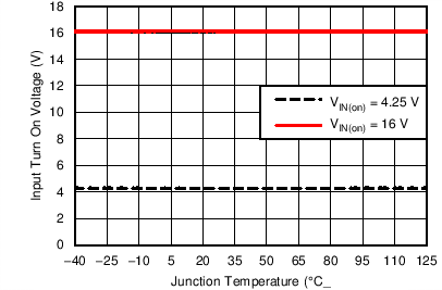
| VIN(on) | Input turn-on voltage(3) | Default settings | 4 | 4.25 | 4.5 | V |
| VIN(off) | Input turn-off voltage(3) | Default settings | 3.8 | 4 | 4.2 | V |
| VINON(rng) | Programmable range for turn on voltage | 4.25 | 16 | V | ||
| VINOFF(rng) | Programmable range for turn off voltage | 4 | 15.75 | V | ||
| ERROR AMPLIFIER | ||||||
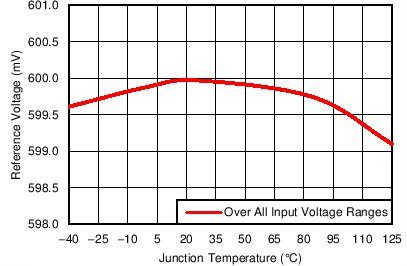
| VFB | Feedback pin voltage | –40°C ≤ TJ ≤ 125°C | 597 | 600 | 603 | mV |
| AOL | Open-loop gain(1) | 80 | dB | |||
| GBWP | Gain bandwidth product(1) | 50 | MHz | |||
| IFB | FB pin bias current (out of pin) | VFB = 0.6 V | 100 | nA | ||
| ICOMP | Sourcing | VFB = 0 V | 1 | mA | ||
| Sinking | VFB = 1 V | 1 | ||||
| BP5 REGULATOR | ||||||
| VBP5 | Output voltage | IBP5 = 10 mA | 4.5 | 5 | 5.5 | V |
| Dropout voltage | VVIN – VBP5, VVDD = 4.5 V, IBP5 = 25 mA |
400 | mV | |||
| IBP5 | Output current | VVDD = 12 V | 40 | mA | ||
| VBP5UV | Regulator UVLO voltage(1) | 3.3 | 3.55 | 3.8 | V | |
| VBP5UV(hyst) | Regulator UVLO voltage hysteresis(1) | 300 | mV | |||
| BP3 REGULATOR | ||||||
| VBP3 | Output voltage | VVDD = 4.5 V, IBP3 ≤ 5 mA | 3.1 | 3.3 | 3.5 | V |
| OSCILLATOR AND RAMP GENERATOR | ||||||
| ƒSW | Adjustment range(1) | 200 | 1500 | kHz | ||
| Switching frequency(4) | RRT = 100 kΩ | 180 | 200 | 220 | kHz | |
| Switching frequency(4) | RRT = 40 kΩ | 450 | 500 | 550 | ||
| Switching frequency(4) | RRT = 13 kΩ | 1230 | 1370 | 1500 | ||
| VRAMP | Ramp amplitude (peak-to-peak) | VVDD/10 | V | |||
| VVAL | Valley voltage | 1.22 | V | |||
| SYNCHRONIZATION | ||||||
| VSYNCH | SYNC high-level threshold(2) | 2 | V | |||
| VSYNCL | SYNC low-level threshold(2) | 0.8 | V | |||
| tSYNC | Minimum SYNC pulse width(1) | 100 | ns | |||
| ƒSYNC | Maximum PWM frequency for SYNC(1) | 1500 | kHz | |||
| Minimum PWM frequency for SYNC(1) | 200 | |||||
| SYNC frequency range (increase from nominal oscillator frequency)(1) | –20% | 20% | ||||
| PWM | ||||||
| VOH(pwm) | PWM high-level output voltage | ILOAD = 500 µA | 4.5 | V | ||
| VOL(pwm) | PWM low-level output voltage | ILOAD = 500 µA | 0.5 | V | ||
| tOFF(min) | Minimum off-time | 100 | ns | |||
| tON(min) | Minimum pulse | 90 | ns | |||
| SOFT-START | ||||||
| tSS | Soft-start time(7) | Factory default settings | 2.7 | ms | ||
| Programmable range(1) | 0.6 | 9 | ms | |||
| Accuracy over range(1) | –15% | 15% | ||||
| tON(dly) | Turn-on delay time(1) | Factory default settings | 0 | ms | ||
| tOFF(dly) | Turn-off delay time(1) | Factory default settings | 0 | ms | ||
| REMOTE SENSE AMPLIFIER | ||||||
| BW | Closed-loop bandwidth(1) | 2 | MHz | |||
| VDIFFO(max) | Maximum DIFFO output voltage | 4.7 | V | |||
| VDIFFO(err) | Error voltage from DIFFO1 to (VSNS1– GSNS1) | (VSNS1– GSNS1) = 1.0 V | –6 | 6 | mV | |
| (VSNS1– GSNS1) = 3.6 V | –19 | 19 | ||||
| IDIFFO | Sourcing | 1 | mA | |||
| Sinking | 1 | |||||
| CURRENT SENSING AMPLIFIER | ||||||
| VCS(mg) | Differential input voltage linear range | (VCSxP – VCSxN), non-smart power mode | 0 | 60 | mV | |
| (VCSxP – VCSxN), smart power mode | 0 | 600 | ||||
| VCS(cmr) | Input common-mode range | Non-smart power mode | 0 | 3.6 | V | |
| VCS(cm) | Input common-mode voltage | Smart power mode | 1.24 | V | ||
| ACS | Current sensing gain | CHx_CSGAIN_SEL= 20 V/V(5), non-smart power mode | 10 | V/V | ||
| CHx_CSGAIN_SEL= 20 V/V(5), smart power mode | 1 | |||||
| fCO | Closed loop bandwidth(1) | 0.66 | MHz | |||
| VCS(chch) | Amplifier output difference between two channels(6) | IPHASE = 20 A, IOUT_CAL_GAIN = 0.503 mΩ | –6% | 6% | ||
| CURRENT LIMIT | ||||||
| tOFF(oc) | Off-time between restart attempts | Hiccup mode | 7 × tSS | ms | ||
| IOC(flt) | Output peak current overcurrent fault threshold | Factory default settings | 40 | A | ||
| Programmable range | 3 | 50 | ||||
| IOC(warn) | Output peak current overcurrent warning threshold | Factory default settings | 37 | A | ||
| Programmable range | 2 | 49 | ||||
| IOC(acc) | Output peak current overcurrent fault accuracy | IOUT = 40 A, IOUT_CAL_GAIN = 0.503 mΩ | –10% | 10% | ||
| Output peak current overcurrent warning accuracy | IOUT = 37 A, IOUT_CAL_GAIN = 0.503 mΩ | –10% | 10% | |||
| PGOOD | ||||||
| VFBPGH | FB PGOOD high threshold | Factory default settings | 642 | mV | ||
| VFBPGL | FB PGOOD low threshold | Factory default settings | 558 | mV | ||
| VPG(acc) | PGOOD accuracy over range | –4% | 4% | |||
| Vpg(hyst) | FB PGOOD hysteresis voltage | 15 | 28 | 45 | mV | |
| RPGOOD | PGOOD pull-down resistance | VFB = 0 V, IPGOOD = 5 mA | 50 | Ω | ||
| IPGOOD(lk) | PGOOD pin leakage current | VFB = 600 mV, VPGOOD = 5 V | 20 | µA | ||
| tPGDELAY | PGOOD delay time after soft-start sequence is complete | Factory default settings | 2 | ms | ||
| OUTPUT OVERVOLTAGE/UNDERVOLTAGE | ||||||
| VFBOV | FB pin over voltage threshold | Factory default settings | 700 | mV | ||
| VFBUV | FB pin under voltage threshold | Factory default settings | 528 | mV | ||
| VUVOV(acc) | FB UV/OV accuracy over range | –4% | 4% | |||
| OUTPUT VOLTAGE TRIMMING AND MARGINING | ||||||
| VFBTM(step) | Resolution of FB steps with trim and margin | 2 | mV | |||
| tFBTM(step) | Transition time per trim or margin step | After soft-start time | 30 | µs | ||
| VFBTM(max) | Maximum FB voltage with trim or margin only | 660 | mV | |||
| VFBTM(min) | Minimum FB voltage with trim or margin only | 480 | mV | |||
| VFBTM(rng) | FB voltage range with trim and margin combined | 420 | 660 | mV | ||
| VFBMH | Margin high FB pin voltage | Factory default settings | 660 | mV | ||
| VFBML | Margin low FB pin voltage | Factory default settings | 540 | mV | ||
| OUTPUT VOLTAGE AT AVS MODE | ||||||
| VFBAVS(step) | Resolution of FB steps at AVS mode | 2 | mV | |||
| VFBAVS(max) | Maximum FB voltage at AVS mode | 1.5 | V | |||
| VFBAVS(min) | Minimum FB voltage at AVS mode | 500 | mV | |||
| AVS INTERFACE | ||||||
| VVIO | ASIC I/O voltage(1) | 1.8 | 2.5 | V | ||
| VIH(avs) | High-level input voltage, AVSCLK, AVSDATA | VVIO = 2.5 V | 1.75 | V | ||
| VVIO = 1.8 V | 1.26 | |||||
| VIL(avs) | Low-level input voltage, AVSCLK, AVSDATA | VVIO = 2.5 V | 0.75 | V | ||
| VVIO = 1.8 V | 0.54 | |||||
| IIH(avs) | High-level input current, AVSCLK, AVSDATA(1) | –50 | 50 | µA | ||
| IIL(avs) | Low-level input current, AVSCLK, AVSDATA(1) | –50 | 50 | µA | ||
| fAVS | AVS clock frequency range | 10 | 30 | MHz | ||
| MEASUREMENT SYSTEM | ||||||
| MVOUT(rng) | VOUT measurement range | 0.5 | 3.6 | V | ||
| MVOUT(acc) | VOUT measurement accuracy(6) | VOUT = 1 V, 0°C ≤ TJ ≤ 125°C | –0.8% | 0.8% | ||
| MIOUT(rng) | IOUT measurement range(9) | 0 | 50 | A | ||
| MIOUT(acc) | IOUT measurement accuracy(6) | IOUT ≥ 20 A, IOUT_CAL_GAIN = 0.503 mΩ, 0°C ≤ TJ ≤ 125°C, smart power mode |
–640 | 640 | mA | |
| PMBus INTERFACE(8) | ||||||
| VIH | High-level input voltage, CLK, DATA, CNTL | 2.1 | V | |||
| VIL | Low-level input voltage, CLK, DATA, CNTL | 0.8 | ||||
| IIH | High-level input current, CLK, DATA, CNTL | Pin voltage = 3.3 V | –10 | 10 | µA | |
| IIL | Low-level input current, CLK, DATA, CNTL | Pin voltage = 0 V | –10 | 10 | ||
| VOL | Low-level output voltage, DATA, SMBALRT | IOUT = 4 mA | 0.4 | V | ||
| IOH | High-level output open drain leakage current, DATA, SMBALRT | VOUT = VBP5 | 0 | 10 | µA | |
| IOL | Low-level output open drain current, DATA, SMBALRT | 4 | mA | |||
| COUT | Pin capacitance, CLK, DATA(1) | 1 | pF | |||
| fPMB | PMBus operating frequency range | Slave mode | 10 | 400 | kHz | |
| tBUF | Bus free time between START and STOP(1) | 1.3 | µs | |||
| tHD:STA | Hold time after repeated START(1) | 0.6 | ||||
| tSU:STA | Repeated START set-up time(1) | 0.6 | ||||
| tSU:STO | STOP setup time(1) | 0.6 | ||||
| tHD:DAT | Data hold time(1) | Receive mode | 0 | ns | ||
| Transmit mode | 300 | |||||
| tSU:DAT | Data setup time(1) | 100 | ||||
| tTIMEOUT | Error signal/detect(1) | 25 | 35 | ms | ||
| tLOW:MEXT | Cumulative clock low master extend time(1) | 10 | ms | |||
| tLOW:SEXT | Cumulative clock low slave extend time(1) | 25 | ms | |||
| tLOW | Clock low time(1) | 1.3 | µs | |||
| tHIGH | Clock high time(1) | 0.6 | µs | |||
| tFALL | CLK/DATA fall time(1) | 300 | ns | |||
| tRISE | CLK/DATA rise time(1) | 300 | ||||
| tRETENTION | Retention of configuration parameters(1) | TJ = 25°C | 100 | Year | ||
| Write_cycles | Number of nonvolatile erase/write cycles(1) | TJ = 25°C | 20 | K cycle | ||
| PMBus ADDRESSING | ||||||
| IADD | Address pin bias current | 8.775 | 9.75 | 10.725 | µA | |
| INITIALIZATION TIME | ||||||
| tINI | Initialization time after BP3 voltage is ready(1) | 1 | ms | |||
| TEMPERATURE SENSE AND THERMAL SHUTDOWN | ||||||
| TSD | Junction shutdown temperature(1) | 160 | °C | |||
| THYST | Thermal shutdown hysteresis(1) | 20 | ||||
| ITSNS(ratio) | Ratio of bias current flowing out of TSNS pin, state 2 to state 1 | Non-smart power mode | 9.7 | 10 | 10.3 | |
| ITSNS(1) | State 1 current out of TSNS pin | Non-smart power mode | 10 | µA | ||
| ITSNS(2) | State 2 current out of TSNS pin | Non-smart power mode | 100 | µA | ||
| TSNS(acc) | External temperature sense accuracy(6) | –40°C ≤ TSNS ≤ 125°C, Non-smart power mode | –4.5 | 4.5 | °C | |
| –40°C ≤ TSNS ≤ 125°C, Smart power mode | –3 | 3 | ||||
| TOT(flt) | Overtemperature fault limit(1) | Factory default settings | 145 | °C | ||
| OT fault limit range(1) | 120 | 165 | ||||
| TOT(warn) | Overtemperature warning limit(1) | Factory default settings | 125 | °C | ||
| OT warning limit range(1) | 100 | 140 | ||||
| TOT(step) | OT fault/warning step | 1 | °C | |||
| TOT(hys) | OT fault/warning hysteresis(1) | 20 | °C | |||
(1) Specified by design. Not production tested.
(2) The external SYNC pin signal must be a square waveform with 50% duty cycle.
(3) Hysteresis of at least 150 mV is specified by design.
(4) Apply to 1-,2- or 4-phase operation. For 3-phase operation, the switching frequency is 33% higher than the value in the table.
(5) Refer to PMBus command MFR_SPECIFIC_21 (OPTIONS) (E5h) section.
(6) Performance verified under application conditions.
(7) The soft-start time is the time that the internal reference voltage rises from 0 V to 600 mV.
(8) The device supports both 100-kHz and 400-kHz bus speeds. The PMBus timing parameters in this table is for operation at 400 kHz. If the PMBus operating frequency is 100 kHz, refer to SMBus specification for timing parameters.
(9) The actual measurement range is limited by IOUT_CAL_GAIN command. See the IOUT_CAL_GAIN (38h) section.
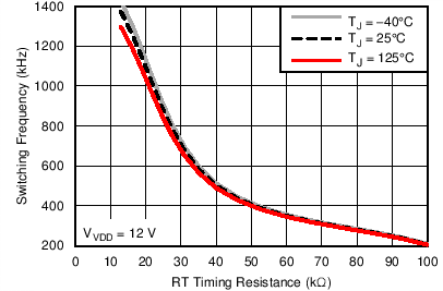
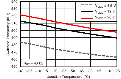
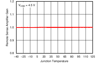
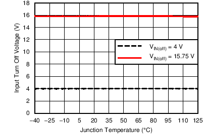
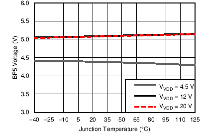
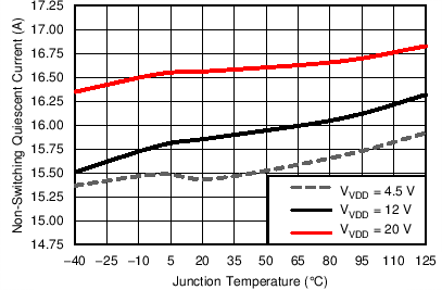
6.6 Typical Characteristics
| Smart-power mode |

| VOUT = 600 mV | Default threshold settings | |