JAJSBU0F July 2012 – November 2020 TPS54020
PRODUCTION DATA
- 1 特長
- 2 アプリケーション
- 3 概要
- 4 Revision History
- 5 Description (Continued)
- 6 Pin Configuration and Functions
- 7 Specifications
-
8 Detailed Description
- 8.1 Overview
- 8.2 Functional Block Diagram
- 8.3
Feature Description
- 8.3.1 Fixed Frequency PWM Control
- 8.3.2 Input Voltage and Power Input Voltage Pins (VIN and PVIN)
- 8.3.3 Voltage Reference (VREF)
- 8.3.4 Adjusting the Output Voltage
- 8.3.5 Safe Start-up into Prebiased Outputs
- 8.3.6 Error Amplifier
- 8.3.7 Slope Compensation
- 8.3.8 Enable and Adjusting Undervoltage Lockout
- 8.3.9 Adjustable Switching Frequency and Synchronization (RT/CLK)
- 8.3.10 Soft-Start (SS) Sequence
- 8.3.11 Power Good (PWRGD)
- 8.3.12 Bootstrap Voltage (BOOT) and Low Dropout Operation
- 8.3.13 Sequencing (SS)
- 8.3.14 Output Overvoltage Protection (OVP)
- 8.3.15 Overcurrent Protection
- 8.3.16 Thermal Shutdown
- 8.4 Device Functional Modes
-
9 Application and Implementation
- 9.1 Application Information
- 9.2
Typical Application
- 9.2.1 Design Requirements
- 9.2.2
Detailed Design Procedure
- 9.2.2.1 Custom Design With WEBENCH® Tools
- 9.2.2.2 Operating Frequency
- 9.2.2.3 Output Inductor Selection
- 9.2.2.4 Output Capacitor Selection
- 9.2.2.5 Input Capacitor Selection
- 9.2.2.6 Soft-Start Capacitor Selection
- 9.2.2.7 Bootstrap Capacitor Selection
- 9.2.2.8 Undervoltage Lockout Set Point
- 9.2.2.9 Output Voltage Feedback Resistor Selection
- 9.2.2.10 Compensation Component Selection
- 9.2.3 Application Curves
- 10Power Supply Recommendations
- 11Layout
- 12Device and Documentation Support
- 13Mechanical, Packaging, and Orderable Information
パッケージ・オプション
メカニカル・データ(パッケージ|ピン)
- RUW|15
サーマルパッド・メカニカル・データ
- RUW|15
発注情報
9.2.2.4.1 Response to a Load Transient
The desired response to a load transient is the first criteria. The output capacitor needs to supply the load with the required current when not immediately provided by the regulator. When the output capacitor supplies load current, the impedance of the capacitor greatly affects the magnitude of voltage deviation during the transient.
In order to meet the requirements for control loop stability, this peak current mode regulator requires the addition of compensation components in the design of the error amplifier. While these compensation components provide for a stable control loop, they often also reduce the speed with which the regulator can respond to load transients. The delay in the regulator response to load changes can be two or more clock cycles before the control loop reacts to the change. During that time, the difference between the old and the new load current must be supplied (or absorbed) by the output capacitance. The output capacitor impedance must be designed to be able to supply or absorb the delta current while maintaining the output voltage within acceptable limits. Equation 22 calculates the minimum capacitance necessary to limit the voltage deviation based on a delay of two switching cycles.
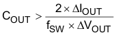
where
- ΔIOUT is the change in output current
- fSW is the switching frequency
- ΔVOUT is the allowable change in the output voltage
For this example, the transient load response is specified as a 5% change in VOUT for a load step of 5 A. For this example, ΔIOUT = 5 A and ΔVOUT = 0.05 × 1.8 = 0.09 V. Using these numbers gives a minimum capacitance of 222 μF. This value does not take the ESR of the output capacitor into account in the output voltage change. For ceramic capacitors, the ESR is usually small enough to ignore in this calculation.