JAJSBU0F July 2012 – November 2020 TPS54020
PRODUCTION DATA
- 1 特長
- 2 アプリケーション
- 3 概要
- 4 Revision History
- 5 Description (Continued)
- 6 Pin Configuration and Functions
- 7 Specifications
-
8 Detailed Description
- 8.1 Overview
- 8.2 Functional Block Diagram
- 8.3
Feature Description
- 8.3.1 Fixed Frequency PWM Control
- 8.3.2 Input Voltage and Power Input Voltage Pins (VIN and PVIN)
- 8.3.3 Voltage Reference (VREF)
- 8.3.4 Adjusting the Output Voltage
- 8.3.5 Safe Start-up into Prebiased Outputs
- 8.3.6 Error Amplifier
- 8.3.7 Slope Compensation
- 8.3.8 Enable and Adjusting Undervoltage Lockout
- 8.3.9 Adjustable Switching Frequency and Synchronization (RT/CLK)
- 8.3.10 Soft-Start (SS) Sequence
- 8.3.11 Power Good (PWRGD)
- 8.3.12 Bootstrap Voltage (BOOT) and Low Dropout Operation
- 8.3.13 Sequencing (SS)
- 8.3.14 Output Overvoltage Protection (OVP)
- 8.3.15 Overcurrent Protection
- 8.3.16 Thermal Shutdown
- 8.4 Device Functional Modes
-
9 Application and Implementation
- 9.1 Application Information
- 9.2
Typical Application
- 9.2.1 Design Requirements
- 9.2.2
Detailed Design Procedure
- 9.2.2.1 Custom Design With WEBENCH® Tools
- 9.2.2.2 Operating Frequency
- 9.2.2.3 Output Inductor Selection
- 9.2.2.4 Output Capacitor Selection
- 9.2.2.5 Input Capacitor Selection
- 9.2.2.6 Soft-Start Capacitor Selection
- 9.2.2.7 Bootstrap Capacitor Selection
- 9.2.2.8 Undervoltage Lockout Set Point
- 9.2.2.9 Output Voltage Feedback Resistor Selection
- 9.2.2.10 Compensation Component Selection
- 9.2.3 Application Curves
- 10Power Supply Recommendations
- 11Layout
- 12Device and Documentation Support
- 13Mechanical, Packaging, and Orderable Information
パッケージ・オプション
メカニカル・データ(パッケージ|ピン)
- RUW|15
サーマルパッド・メカニカル・データ
- RUW|15
発注情報
8.3.8 Enable and Adjusting Undervoltage Lockout
The EN pin provides electrical on and off control of the device. Once the EN pin voltage exceeds the threshold voltage, the device starts operation. If the EN pin voltage is pulled below the threshold voltage, the regulator stops switching and enters low quiescent state. The EN pin has an internal hysteretic current source, allowing the user to design the ON and OFF threshold voltages with a resistor divider at the EN pin. If an application requires controlling the EN pin, use open drain or open collector output logic to interface with the pin.
The EN pin can be configured as shown in Figure 8-1, Figure 8-2, and Figure 8-3. It is recommended to set the UVLO hysteresis to be greater than 500 mV to avoid repeated chatter during start-up or shutdown. The EN pin has a small fixed pullup current iP which sets the current source value before the start-up sequence. The device includes the second current source iH when the threshold voltage has been exceeded. To achieve clean transitions between the OFF and ON states, TI recommendeds that the turn OFF threshold is no less than 4.2 V, and the turn ON threshold is no less than 4.4 V on the VIN pin.
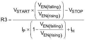
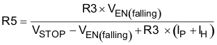
The UVLO thresholds can be calculated using Equation 2 and Equation 3.
 Figure 8-1 Adjustable VIN Undervoltage Lockout
 Figure 8-3 Adjustable VIN and PVIN Undervoltage Lockout
 Figure 8-2 Adjustable PVIN Undervoltage Lockout, PVIN ≥ 4.5 V
R3, the top UVLO divider resistor, is calculated using Equation 2.
R5, the bottom UVLO divider resistor, is calculated in Equation 3.
In this example:
- IH = 3.3 μA
- IP = 1.15 μA
- VENRISING = 1.22 V
- VENFALLING = 1.17 V